Empirical model integration for accurate charge carrier mobility simulation in silicon MOSFETs
-
Elhouaria Bourbaba
 ,
Syham Kadri
,
Mohammed Bensafi
,
Syham Kadri
,
Mohammed Bensafi
 ,
Badr M. Alshammari
,
Badr M. Alshammari

Abstract
This study investigates the use of combined empirical models to improve charge carrier mobility simulation in silicon MOSFETs, overcoming the limitations of conventional single-model approaches. With continued device miniaturization, accurate mobility modeling is essential to capture interactions among temperature, doping concentration, electric fields, and scattering mechanisms. Three hybrid modeling strategies are assessed, (i) Power Law–Lombardi, (ii) Arora–Lombardi–Caughey-Thomas, and (iii) Arora–Fletcher–Lombardi–Caughey-Thomas, against a baseline power-law model. Numerical results indicate that the Arora–Lombardi–Caughey-Thomas combination achieves the best balance between accuracy and computational efficiency, effectively representing doping, temperature, and high-field effects. Validation with experimental data confirms the model’s predictive reliability. The findings emphasize the advantage of integrating empirical models to enhance both precision and performance in MOSFET simulations.
1 Introduction
Continuous progress in semiconductor device technology has driven the scaling of metal–oxide–semiconductor field-effect transistors (MOSFETs) into nanometer regimes, where classical models fail to capture the increasingly complex physical behaviors. Among emerging power semiconductor technologies, silicon carbide (SiC) and gallium nitride (GaN) have demonstrated outstanding capabilities in high-frequency, high-voltage, and high-temperature environments owing to their wide bandgap, high critical electric field, and excellent thermal conductivity [1], [2], [3], [4]. Bonkoungou et al. [1] developed a semi-physical EKV model for SiC MOSFETs capable of describing nonlinear switching behavior, while Shankari et al. [2] examined vertical GaN MOSFET architectures to enhance device robustness under elevated thermal stress. Dai et al. [3] provided transient electrothermal insights into SiC devices, and Er-rafii and Galadi [4] formulated a temperature-scalable DC model that accurately predicts electrical characteristics over broad operational ranges.
The necessity for high-reliability and radiation-tolerant power devices has also intensified. Peng et al. [5] explored the impact of total ionizing dose (TID) effects in poly-Si thin-film transistors (TFTs), whereas Shen and Yuan [6] applied Green’s function-based methods to investigate low-frequency noise mechanisms in MOSFETs. In the context of nanoscale biosensors, Ding et al. [7] introduced a junctionless cylindrical surrounding-gate (JLCSG) MOSFET integrating quantum confinement effects for enhanced sensing precision. Cabré et al. [8] developed a semi-empirical predictive model for double-gate MOSFETs that effectively couples electrostatics and carrier transport, and Wong [9] presented a universal framework for carrier mobility modeling, emphasizing its dependency on vertical electric fields.
Quantum mechanical effects have been increasingly incorporated into analytical MOSFET formulations to enhance physical accuracy. Peng et al. [10] developed a compact model for nanoscale gate-all-around MOSFETs that explicitly accounts for quantum confinement, while Ortiz-Conde et al. [11] derived a rigorous surface potential equation based on Fermi–Dirac statistics using polylogarithmic functions, thereby improving predictive precision for deep submicron devices. Similarly, Ghosh [12] proposed an analytical framework for short-channel, fully depleted silicon-on-insulator (SOI) MOSFETs, revealing how geometry scaling influences inversion charge and electrostatic control. Alessandrini et al. [13] extended this concept by developing a comprehensive mobility model for both single- and double-gate SOI MOSFETs, validated against experimental data. Ye et al. [14] conducted a two-dimensional simulation study on silicon power MOSFETs operating at low temperatures, highlighting the importance of temperature-dependent transport models for accurately describing carrier dynamics and device performance. Balaguer et al. [15] modeled inversion charge in double-gate MOSFETs, while Baral et al. [16] introduced a unified two-dimensional model for nanowire junctionless MOSFETs with strong electrostatic coupling.
Moldovan et al. [17] presented compact charge and capacitance models applicable to modern transistor geometries, and Roldán and Gámiz [18] analyzed strained-Si/SiGe structures to understand mobility enhancement mechanisms. In parallel, Toan and Maity [19] developed physics-based models for III–V double-gate MOSFETs, while Palestri et al. [20] applied semi-classical Monte Carlo simulations to study transport behavior under nanoscale confinement. Madheswaran et al. [21] investigated hot-carrier reliability and optical properties of advanced MOSFET structures, and He et al. [22] presented the BSIM5 model, an advanced charge-based MOSFET model developed for accurate nanoscale VLSI circuit simulation.
Further developments have focused on channel material engineering and quantum confinement. Bhattacherjee and Biswas [23] analyzed long-channel germanium double-gate p-MOSFETs with high-k dielectrics, showing that dielectric–semiconductor interface quality and carrier effective mass significantly affect subthreshold behavior. Osgnach et al. [24] examined the impact of interface states on electron mobility in InGaAs MOSFETs, while Cerdeira et al. [25] proposed a compact model for doped short-channel double-gate devices. Wang et al. [26] developed a compact model to account for quantum effects in symmetric double-gate MOSFETs, while Fei et al. [27] investigated the temperature limitations and failure mechanisms of SiC MOSFETs under avalanche conditions, emphasizing the thermal–electrical trade-offs at high bias operation.
Venugopalan et al. [28] developed the BSIM-CG compact model for cylindrical and surround-gate MOSFETs, incorporating a surface potential-based formulation with quantum confinement effects. Ratnesh et al. [29] reviewed the scaling challenges in MOSFET technologies, emphasizing performance degradation caused by short-channel, tunneling, and threshold voltage effects, whereas Sharma et al. [30] proposed a subthreshold model addressing gate misalignment in double-gate architectures. Sai et al. [31] extended DC and RF modeling to cryogenic InGaAs MOSFETs, and Dastjerdy et al. [32] implemented three-dimensional non-equilibrium Green’s function (NEGF) simulations for nanowire MOSFETs to elucidate quantum transport. Ghosh et al. [33] developed a drain current model incorporating drain-induced barrier lowering for dual-material cylindrical and surround-gate MOSFETs, demonstrating enhanced drain current, reduced output conductance, and superior performance over single-gate counterparts.
At the device physics level, Takagi et al. [34] and Lee [35] investigated the universal mobility–electric field relationship, while Jeon and Burk [36] and Chen et al. [37] formulated physically based semi-empirical models for drain current and inversion charge density. Li et al. [38] proposed an overcurrent protection integrated circuit (IC) to enhance SiC MOSFET reliability, and Wang et al. [39] experimentally and numerically investigated heavy-ion irradiation effects on p- and n-channel power UMOSFETs, analyzing leakage current degradation and single-event failure mechanisms such as burnout and gate rupture.
Despite substantial progress in both empirical and physics-based modeling, achieving a unified and accurate description of charge carrier mobility in silicon MOSFETs remains a critical challenge. Conventional single-model formulations often struggle to account for the complex interplay among temperature, doping concentration, electric field, and various scattering mechanisms. As device geometries continue to shrink, these limitations become increasingly pronounced, leading to deviations in simulated performance compared to experimental observations. Furthermore, balancing physical accuracy with computational efficiency remains a persistent concern, particularly in large-scale circuit simulations where model stability and predictive reliability are essential. These challenges underscore the need for refined mobility models capable of integrating multiple empirical formulations to enhance both precision and consistency across operating conditions.
The primary aim of this study is to develop and evaluate combined empirical modeling approaches to improve the accuracy of charge carrier mobility simulation in silicon MOSFETs. Three hybrid models, Power Law–Lombardi, Arora–Lombardi–Caughey-Thomas, and Arora–Fletcher–Lombardi–Caughey-Thomas, are formulated and assessed against a baseline power-law model. The objective is to identify an optimal hybrid configuration that provides a robust representation of temperature, doping concentration, electric field, and scattering effects while maintaining computational efficiency. Validation against experimental data ensures that the proposed hybrid models deliver reliable predictive capability, offering a pathway toward more precise and efficient MOSFET performance simulation.
2 Mathematical modeling
2.1 Device structure and parameters
A silicon-based MOSFET is an electrical device composed of multiple material layers designed to regulate the flow of electric current. The basic structure of an n-channel MOSFET begins with a p-type doped silicon substrate. On this substrate, two heavily doped n + regions are formed to create the source and drain, which serve as the injection and collection terminals for charge carriers, respectively. The channel region lies between the source and drain, and its conductivity is controlled by the gate voltage. A thin silicon dioxide (SiO2) layer acts as the gate oxide, providing electrical insulation between the gate and the channel, while a conductive polysilicon electrode forms the gate itself. When a voltage is applied to the gate, an electric field is established, attracting charge carriers to the substrate surface and creating a conductive path between the source and drain. Finally, metal contacts are deposited on the source, drain, and gate to enable external electrical connections. Owing to its simple yet highly efficient design, the MOSFET functions as both a switch and an amplifier in modern electronic circuits.
In this study, the MOSFET model employs a simplified 2D geometry with an overall device size of approximately 3 µm in width and 0.7 µm in height, representing a cross-sectional view as shown in Figure 1. The gate oxide interface maintains continuity of the electric displacement field. Trap-assisted recombination is represented using the Shockley–Read–Hall model, which describes the recombination of electrons and holes via defect states within the band gap, thereby enabling precise simulation of carrier behavior in the MOSFET. An overview of the parameters and silicon characteristics used in our simulation is provided in Table 1, with further details available in references [40], [41], [42], [43].
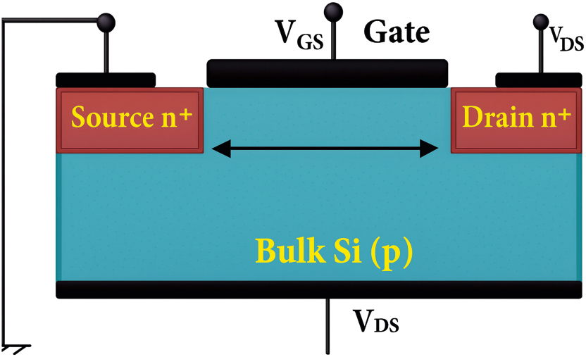
Abstract diagram of an N-channel transistor highlighting essential electrical connections.
Key parameters and material properties of silicon.
| Parameters | Value [40], [41], [42], [43] |
|---|---|
| Silicon properties | |
| Relative permittivity (ɛ rnSi) | 11.5 |
| Band gap (E g , eV) | 1.12 |
| Intrinsic carrier concentration (n i , 1/cm3) | 1.5 × 10¹⁰ |
| Electron affinity (χ, eV) | 4.05 |
| Source/drain doping (N D , 1/cm3) | 1020 |
| Substrat doping (N A , 1/cm3) | 1017 |
| Oxide properties | |
| Relative permittivity (ɛ rnox) | 4.5 |
| Thickness (d, nm) | 30 |
2.2 Carrier transport model and governing equations
The Boltzmann Transport Equation (BTE) serves as the theoretical foundation for understanding transport phenomena, describing the evolution of the charge carrier distribution function under disequilibrium conditions [44], 45]. In practice, device simulations frequently use the drift-diffusion approximation because of the intricacy of the Boltzmann equation [46], 47]. This approach, based on the assumption of local carrier equilibrium, represents charge transport as the combined effects of drift, driven by an electric field, and diffusion, resulting from concentration gradients [48], 49]. Models derived from this approximation significantly reduce computational time while maintaining the flexibility to study non-equilibrium transport in MOSFETs. However, empirical mobility models are necessary to accurately capture the influence of electric fields, and a more precise formulation is required for describing high-field transport and carrier diffusion [50], 51].
Here, the main charge transport equations in the drift–diffusion approximation are presented, namely the continuity and Poisson equations. Electron and hole continuity equations are expressed as [48]:
where G n and G p represent the generation and recombination rates of electron–hole pairs. The drift–diffusion current densities for electrons and holes are given as [46], 52]:
Finally, the electric field (E) is determined using Poisson’s equation [46]:
Equations (1)– (4) are coupled with Poisson’s equation (5). It is important to note that the carrier mobilities μ n and μ p are not constant; they depend on temperature, electric field, doping concentration, and other physical factors.
2.3 Effective mobility
The MOSFET operates by modulating the conductivity of a semiconductor channel, typically silicon, through an electric field induced by the gate voltage. When the gate voltage exceeds a certain threshold, an inversion layer is formed at the semiconductor–oxide interface, enabling current to flow between the source and drain regions. The carrier mobility within this inversion layer is significantly lower than that in the bulk semiconductor and is referred to as the effective mobility (μ eff). Charge transport in the channel is influenced by several scattering mechanisms, including phonon interactions, interface roughness at the gate oxide, Coulomb scattering from charged impurities, and structural defects, which collectively degrade mobility and device performance.
Three primary scattering mechanisms can be identified that limit carrier mobility. Each mechanism is influenced differently by factors such as temperature, transverse electric field, doping concentration, and other material or device parameters [34], 36], 53].
Coulomb interactions, with charged impurities, limit mobility at low field.
Interactions with phonons, for a temperature lower than 100 K; this type of collision is due to vibrations of the crystal lattice [54].
Mobility is limited by collisions caused by surface roughness (channel/gate dielectric interface), particularly at high fields, because the carriers are trapped close to the interface.
Usually, mobility is described, as a first approximation, by Matthiessen’s law (valid at low source–drain electric fields). This law assumes independent scattering mechanisms, allowing the probabilities of collisions with Coulomb centers (cb), surface roughness (sr), and phonons (ph) to be summed [48]:
that is,
The relaxation time (τ) takes into account all the interactions that the carriers may undergo during transport, where i correspond to the relaxation time for a particular interaction [36]:
These parameters are determined using empirical models, which will be discussed in the following section, as the effects of small-scale physical phenomena are incorporated into the large-scale mobility used in transport equations.
2.4 Limitations of individual empirical mobility models
One of the most important parameters for describing charge carrier movement and current formulation in semiconductor devices is the electron and hole mobility, denoted as μ n and μ p , respectively. These mobilities have a significant impact on the electrical characteristics of MOSFETs. Various mobility models have been proposed in the literature to describe MOSFET behavior [55]. A few commonly used carrier mobility models are outlined below.
2.4.1 Power law model
Early studies of mobility introduced simple formulations such as the power law model [43]. This model, characterized by its simplicity, expresses the dependence of mobility on temperature through a power-law relationship [46]:
This model was commonly used in early device simulations when computational limitations restricted model complexity. However, its accuracy is limited because it neglects the effects of doping concentration and electric field dependence.
2.4.2 Caughey–Thomas model
The 1960s saw the emergence of more sophisticated models, notably the Caughey–Thomas model. This model introduced the influence of the electric field on carrier mobility [56], simulating the saturation of carrier velocity under strong electric fields. The model is expressed as:
The default approach for calculating the saturation velocities incorporates temperature dependence and is defined as:
The default reference temperature is T ref = 300 K. The dimensionless material parameters, β n,0, β p,0, α 1,n , α 1,p , α 2,n , and α 2,p , are obtained from experimental data. By accounting for velocity saturation, this model became fundamental for simulating short-channel devices. However, it does not include the effects of doping concentration or detailed temperature dependence.
2.4.3 Arora et al.’s carrier mobility model
This model is temperature-dependent and includes both phonon and impurity scattering [57]. It is used to simulate the doping-dependent mobility:
with:
and
This model, while remaining relatively simple, has become a valuable tool for power device simulations in which doping plays a crucial role. However, it remains limited as it does not account for the dependence on the electric field.
2.4.4 Lombardi model
The late 1980s marked a turning point with the introduction of the Lombardi model [58], a semi-empirical formulation grounded in physical principles to describe the scattering mechanisms influencing carrier mobility. It accounts for phonon scattering, ionized impurity scattering, and interface roughness effects. The general expression applies Matthiessen’s rule to combine these mechanisms as follows:
where
with
This model provides a more accurate fit to experimental data and a deeper physical understanding of the underlying transport phenomena. However, it is more complex to implement than earlier empirical models and requires careful parameter calibration to achieve optimal accuracy.
2.4.5 Dorkel–Leturg model
This model is used to describe scattering effects caused by thermally excited acoustic phonons, doping impurities, and carrier–carrier interactions [59]. Carrier–carrier scattering mobility (μ ccs ) becomes particularly relevant under high carrier concentrations. The following equation defines this model [59]:
which accounts for lattice or phonon scattering effects on electron and hole mobility, also known as lattice mobility (μ L ). Here, μ L0 and α depend on the dopant type and temperature range, while T represents the lattice temperature. When both carrier types are present in high densities, carrier–carrier scattering mobility (μ ccs ) becomes significant, and the Fletcher mobility model can be applied [60]:
to describe the effect of carrier–carrier interactions on overall mobility.
To account for interactions between charge carriers and ionized impurities, impurity mobility (μ I ) is introduced [59]:
where N denotes the doping concentration, and A and B are parameters dependent on the dopant type.
These models provide analytical expressions capturing mobility reduction due to enhanced phonon interactions at elevated temperatures, increased ionized impurity scattering at higher doping levels, and carrier–carrier interactions under high injection conditions. They are particularly useful for simulating devices where high injection effects are important. However, the models have limitations: they rely on simplified representations of scattering mechanisms, exhibit limited accuracy under high electric fields, assume a relatively homogeneous semiconductor, and depend on parameters fitted to experimental data. As such, they are primarily designed for silicon devices and are less accurate for high-field transport modeling.
2.5 Combining empirical mobility models
Charge transport in semiconductors involves multiple physical mechanisms, which cannot be fully captured by a single mobility model. Combining several models enables a more comprehensive description of how carrier mobility is influenced by temperature, doping concentration, electric fields, and scattering processes. In this work, we adopt a hybrid modeling approach, evaluating multiple combinations of empirical models to generate different scenarios and assess their effectiveness in accurately predicting MOSFET behavior.
2.5.1 Scenario (i): combined power Law–Lombardi model
The first scenario employs a hybrid approach that combines the Power Law and Lombardi models. The Power Law model calculates a baseline low-field mobility that depends on temperature, which is then used as a key input for the more physically detailed Lombardi model as shown in Figure 2. The Lombardi model refines this baseline by accounting for the effects of phonon scattering, ionized impurity scattering, and surface roughness scattering. This combination provides a computationally efficient and reasonably accurate representation of carrier mobility, capturing both temperature dependence and multiple scattering mechanisms. The resulting mobility is subsequently used in the carrier transport equations for device simulation.
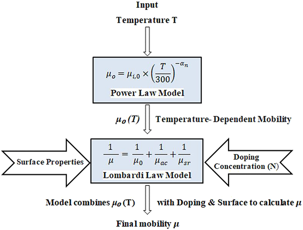
Model integrating various scattering processes.
2.5.2 Scenario (ii): combined Arora, Lombardi, and Caughey-Thomas models
The combination of the Arora, Lombardi, and Caughey-Thomas mobility models provides a comprehensive approach for modeling charge transport in MOSFET structures, capturing a wide range of physical effects as illustrated in Figure 3. The Arora model establishes a foundational description of mobility, accounting for temperature and doping concentration dependence, which is essential for accurate simulation across different operating conditions and device doping profiles. According to this, the Lombardi model enhances the mobility computation by adding the physically-based mechanisms of scattering, i.e., phonon, ionized impurity, and surface roughness scattering, and thus improves the reliability of simulations within the channel area. The Caughey-Thomas model addresses the limitations of the previous two models under high electric field conditions by modeling velocity saturation, which is particularly important in short-channel MOSFETs near the drain region.
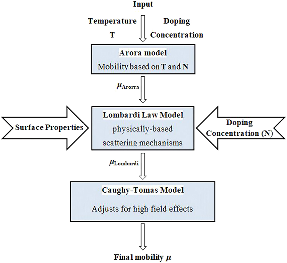
Model incorporating temperature, doping, and high-field effects.
In this combined approach, the Arora model first provides a baseline mobility value, which is then successively adjusted by the Lombardi model and the Caughey-Thomas model. This cascading methodology captures both high-field and temperature-dependent effects, resulting in a more accurate representation of carrier mobility. The integration of these models enhances the realism of simulation results, providing valuable insights for MOSFET design, analysis, and optimization.
2.5.3 Scenario (iii): combined Arora, Fletcher, Lombardi, and Caughey-Thomas models
To simulate carrier transport accurately across a wide range of operating conditions, a combined mobility modeling approach is employed, integrating the strengths of multiple established models. Building on Fletcher’s work on high-current effects [60], this scenario incorporates injection-level effects into the mobility computation. In this approach, the baseline mobility calculated by the Arora model is first modified by the Fletcher model to account for reductions caused by increased carrier–carrier interactions, and is then further refined by the Lombardi and Caughey-Thomas models, as illustrated in Figure 4. This cascading methodology captures the combined influence of temperature, doping, scattering mechanisms, high electric fields, and injection-level effects, resulting in a comprehensive and realistic representation of carrier transport for semiconductor device simulations.
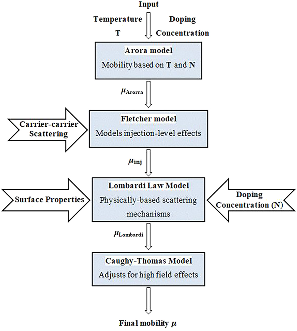
Model combination, by capturing the interplay of temperature, doping, injection level, scattering mechanisms, and electric field effects.
2.6 Empirical model parameterization and calibration
The accuracy of empirical mobility models strongly depends on the proper calibration of numerous adjustable parameters, including minimum electron mobility, minimum hole mobility, low-field electron and hole velocities, and temperature or field exponents. Specifically, parameters such as μ min,p , μ min,n , v n,0, v p,0, β n,0, α 1,n and others play a critical role in defining the behavior of charge carriers under different operating conditions.
The primary objective of this study is to evaluate the structural effectiveness of different model combinations across varying operational regimes, rather than performing device-specific optimization. Consequently, widely accepted standard parameter sets for bulk silicon, derived from extensive experimental fitting data reported in the literature, are employed.
For Scenarios i, ii, and iii, all model coefficients are obtained from the original studies by Caughey-Thomas [56], Arora [57], and Lombardi [58], and correspond to values commonly used in generalized silicon devices. These parameters ensure that the base mobilities, field dependencies, and temperature exponents accurately represent the semi-classical transport behavior of silicon, providing a robust basis for assessing the performance of the combined mobility models.
3 Numerical modeling
3.1 Numerical simulation
The numerical simulation of a two-dimensional Si MOSFET was conducted following a structured workflow to ensure accuracy, reproducibility, and computational efficiency, as outlined in Figure 5. The procedure comprises three sequential phases: Pre-Processing, Solving, and Post-Processing.

Analysis process using a numerical model.
In the Pre-Processing phase, the finite element type, device geometry, material properties, and mobility model parameters were defined, followed by the construction of a two-dimensional device representation and the generation of a computational mesh with local refinement in critical regions. Boundary conditions were imposed, and output variables were specified.
During the solving phase, static or dynamic analysis was selected, and the global matrices and element vectors were assembled over the domain. The coupled nonlinear partial differential equations, encompassing Poisson’s equation for the electrostatic potential and the carrier continuity equations for electrons and holes, were solved iteratively, with convergence criteria rigorously monitored to ensure numerical stability and accuracy.
In the post-processing phase, converged solutions were analyzed both quantitatively and graphically, with additional operations, including interpolation, combination, and derived quantity evaluation, performed to extract relevant physical insights and validate device performance. This methodology ensures that the numerical model reliably captures the electrical characteristics of the MOSFET while minimizing computational errors.
3.2 Numerical validation
Figure 6 illustrates the variation of the calculated effective mobility as a function of the transverse electric field at three distinct lattice temperatures: 133 K (low-temperature regime where phonon scattering is minimal), 297 K (near room temperature), and 447 K (high-temperature regime characterized by dominant phonon scattering). The simulated results (dashed lines) are compared with the experimental data (symbols) reported by Takagi et al. [34] for a substrate doping concentration of 3.9 × 1015 cm−3. The strong agreement between the simulated and experimental data across the examined temperature range validates the accuracy of the developed numerical model. The model accurately reproduces the expected mobility enhancement at 133 K due to the suppression of lattice vibrations and the corresponding reduction in phonon-limited scattering, as well as the significant mobility degradation at 447 K resulting from increased phonon–carrier interactions. This consistency confirms that the implemented combined mobility model provides a reliable physical representation of carrier transport mechanisms under varying thermal conditions.
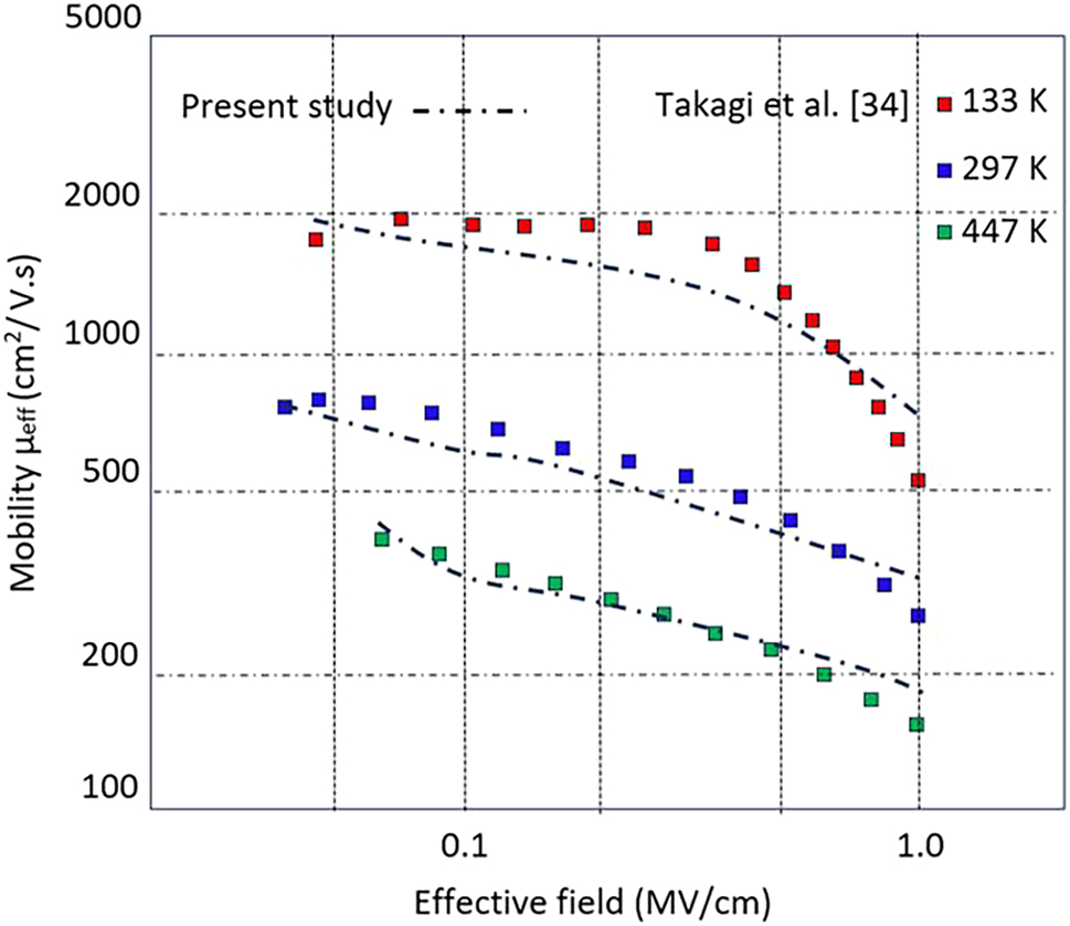
Simulated and experimental effective mobility versus transverse electric field at different lattice temperatures for a substrate doping concentration of 3.9 × 1015 cm−3.
4 Results and discussions
Figure 7 presents the drain current (I d ) versus gate voltage (V g ) characteristics for a MOSFET operating at a low drain voltage of V d = 10 mV, simulated under three different modeling scenarios in addition to the constant mobility case. The curves depict the transistor’s response across both the subthreshold and strong inversion regions. In Figure 7(a), the constant mobility model yields an almost linear behavior but fails to accurately represent the subthreshold conduction and the saturation effects observed in strong inversion. The second configuration (Scenario i), which combines the Power Law model (to account for temperature dependence) and the Lombardi model (to capture surface scattering effects), produces a smoother transition between the subthreshold and strong inversion regions, though minor deviations in leakage current estimation are observed. The third configuration (Scenario ii), which further incorporates the Arora model (doping-dependent mobility) and the Caughey–Thomas model (mobility saturation at high electric fields), improves accuracy by yielding a steeper subthreshold slope and a clearer transition. Finally, the fourth configuration (Scenario iii), which additionally integrates the Fletcher model (for temperature dependence at low temperatures), provides the most comprehensive representation, exhibiting enhanced leakage current prediction and a more pronounced transition between operating regions.
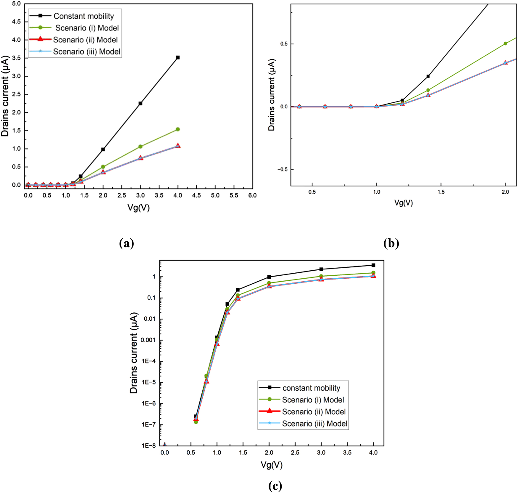
Comparison of I d versus V g characteristics across different combined mobility models: (a) linear-scale plot at low drain bias (V d = 10 mV), (b) zoom-in view around the threshold voltage (V th ), and (c) logarithmic-scale representation highlighting subthreshold behavior.
Figure 7(b), which provides a magnified view around the threshold voltage, shows that the constant mobility model produces a diffuse transition between the subthreshold and strong inversion regions. The first two combined models improve this transition; however, it remains less pronounced than in the third and fourth combined models, where the inclusion of doping- and temperature-dependent effects sharpens the transition and yields a more accurate threshold voltage (V th ).
Figure 7(c), which presents I d on a logarithmic scale, enables clearer visualization of subthreshold currents at low gate voltages and accentuates the distinctions among the mobility models. The influence of the various modeling approaches is evident: while the constant mobility model tends to overestimate or underestimate the leakage current, the third and fourth combined models provide more realistic predictions, particularly under low-temperature conditions, due to their inclusion of both temperature and doping effects. The estimated V th in these models is approximately 1.15 V, closely matching the theoretical value of about 1.27 V [34], 35]. Moreover, the leakage current (I off) is more accurately captured by the third and fourth combined models, ranging between 10−12 A and 10−13 A at low temperatures, whereas the constant mobility and second combined models either overpredict or underpredict this parameter.
Figure 8 displays I d as V d varies with different gate voltages: V g = 2 V in Figure 8(a), 3 V in Figure 8(b), and 4 V in Figure 8(c), simulated under three different scenarios as well as with constant mobility. These curves illustrate the MOSFET’s behavior in both the linear (triode) and saturation regimes, allowing for a visual comparison of the I d –V d characteristics obtained with different models.
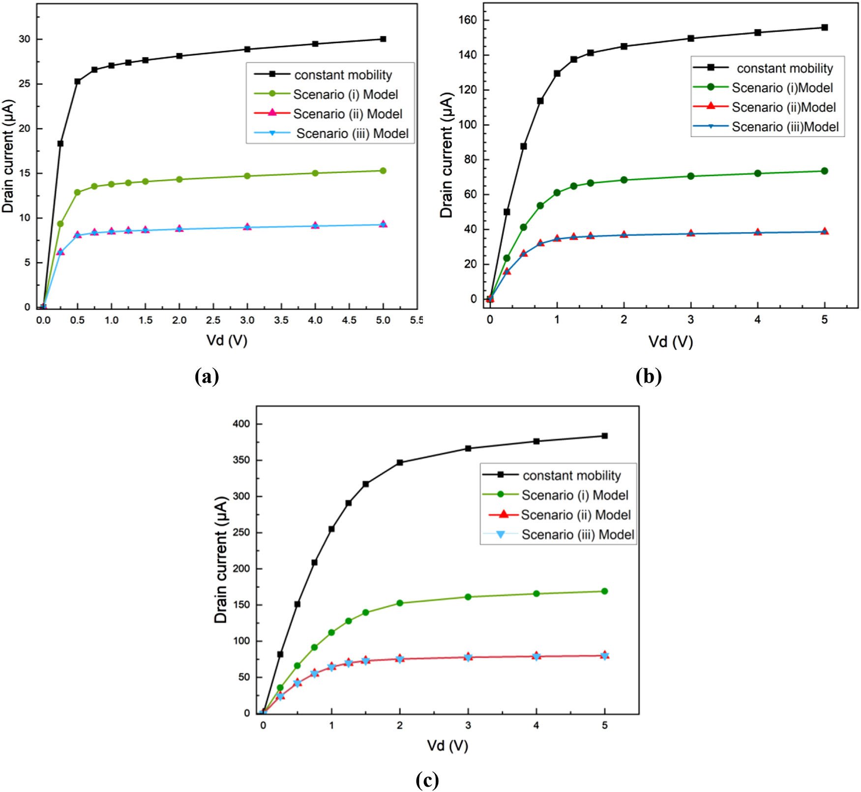
I d versus V d characteristics for various mobility models, illustrating performance in the linear and saturation regimes: (a) V g = 2 V, (b) V g = 3 V, (c) V g = 4 V.
Several key differences can be observed: with constant mobility, the I d –V d curve in the saturation region exhibits a nonzero slope, which is unrealistic. In Scenario (i), the I d –V d curve flattens further in the saturation region but may still not be perfectly horizontal. In Scenarios (ii) and (iii), the I d –V d curve is closer to a horizontal line in the saturation region, aligning more closely with the real-world behavior of a MOSFET. The combined model curves exhibit a shallower slope compared to the constant mobility curve, indicating that mobility is reduced due to the incorporation of mobility models. This figure also highlights the impact of different mobility models on current behavior in the linear region. In the saturation region, the combined mobility models more accurately capture charge carrier velocity saturation, resulting in a more pronounced flattening of the I d –V d curve. Velocity saturation occurs when charge carriers reach a maximum velocity beyond which they can no longer accelerate, even as the electric field continues to increase.
Figure 9(a) shows that the peak electric field near the drain side of the MOSFET increases with increasing drain voltage. As depicted in Figure 9(b), the peak magnitude remains approximately constant across all cases. Figure 9(c) illustrates that the MOSFET structure has been optimized to minimize band-to-band tunneling (BTBT) leakage current, a critical factor in reducing power consumption and enhancing the overall performance and reliability of MOSFET-based circuits.
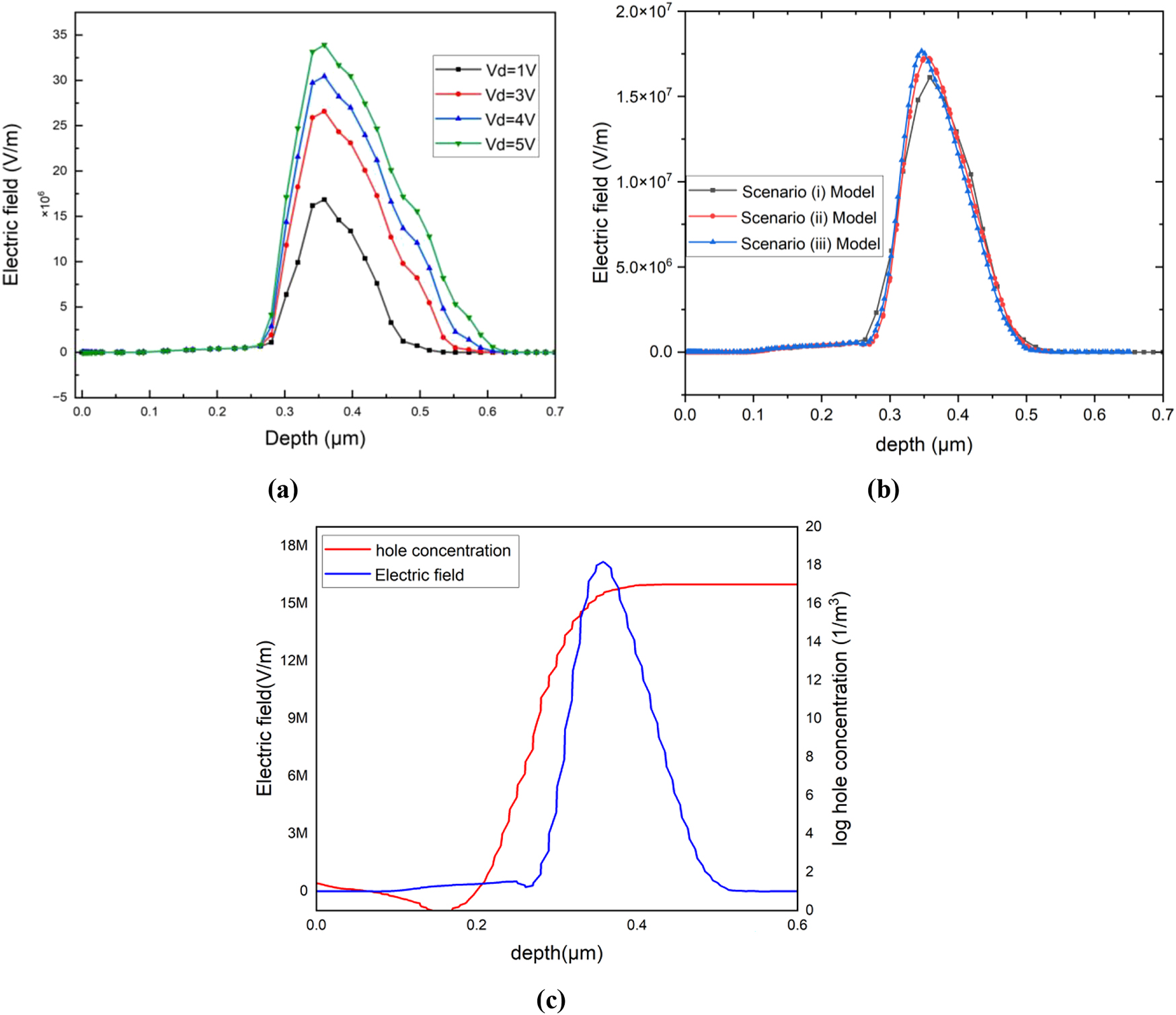
Analysis of the electric field in the MOSFET drain region: (a) peak electric field depth as a function of V d at V g = 4 V, (b) comparison of the electric field depth across the integrated mobility scenarios (i, ii, and iii) at V g = 4 V, (c) electric field and hole concentration profile, demonstrating the optimization for BTBT minimization.
Figure 10 is the log plot of electron concentration versus position in the channel for the three cases. Relative to V g , as V g increases beyond the threshold voltage (V th ), the electron concentration in the channel also increases. In terms of channel position, the concentration is larger near the source and decreases gradually towards the drain, especially at high V d . Near the drain, greater V d reduces the concentration of carriers, eventually leading to pinch-off.
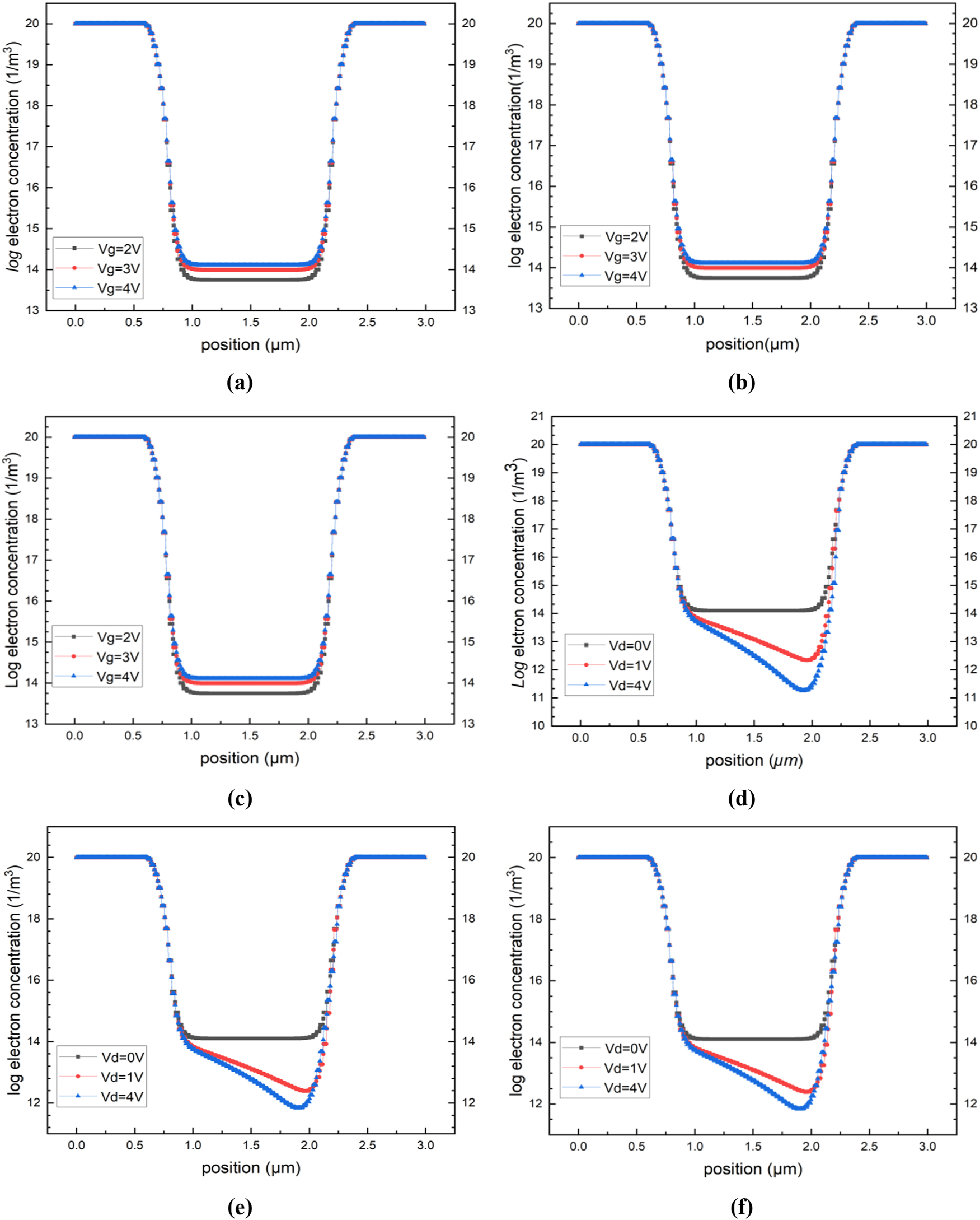
Logarithm of electron concentration profile along the MOSFET channel: (a)–(c) inversion channel formation and density evolution at V d for increasing V g , (d)–(f) impact of increasing V d under a high gate bias (V g = 4 V).
Figure 11 illustrates the electric potential distribution across the channel for various situations, with curves (a–c) showing the potential variation as a function of the V g under a 1 V drain bias. It is evident that the potential drops in the inversion region as the V g increases. Curves (d–f) demonstrate that increasing the V d raises the potential barrier in the drain region. As the drain-to-source voltage (V ds ) rises, an electric field is established along the channel, which accelerates charge carriers from the source toward the drain. This electric field is stronger near the drain than near the source. When V ds reaches a value such that V gs − V ds = V th , the concentration of charge carriers near the drain becomes very low or even zero, causing the channel to ‘pinch off’ near the drain. Although the channel is pinched, current continues to flow due to the electric field between the drain and the pinched region.
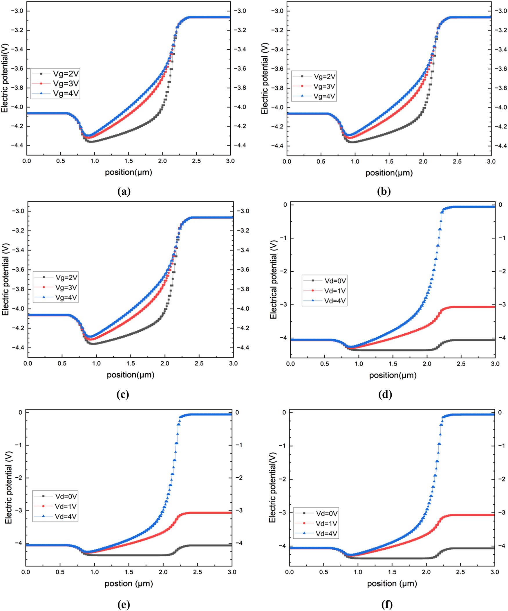
Electric potential distribution across the MOSFET channel: (a)–(c) evolution of the inversion layer potential with increasing V g at a fixed drain bias (V d = 1 V), (d–f) effect of increasing V d under a high gate bias (V g = 4 V).
In the saturation region of the MOSFET, charge carriers are progressively drawn from the channel toward the drain. Under these conditions, the I d becomes nearly independent of the V ds and primarily depends on the V gs . Figure 12 compares the electron concentration and electric potential distributions along the channel at V g = 4 V and V d = 4 V for the three scenarios, assuming constant mobilities. It is important to note that the mobility models significantly influence the redistribution of carriers under the applied voltage, thereby affecting the carrier concentration profile. With constant mobility, the pinch-off occurs abruptly, and the electron concentration drops sharply to zero near the drain region. This approach often yields poor estimates near the drain, as it neglects the effects of doping concentration and high electric fields. In Scenario (i), the carrier concentration is slightly higher than in the constant mobility case, although the near-drain variations remain somewhat underestimated. This model improves accuracy by incorporating temperature and surface scattering effects but omits doping and field-dependent mobility influences. In Scenarios (ii) and (iii), where field-dependent mobility models are employed, the pinch-off behavior becomes more gradual, with the carrier concentration decreasing progressively toward the drain, providing a more realistic representation of the physical process.
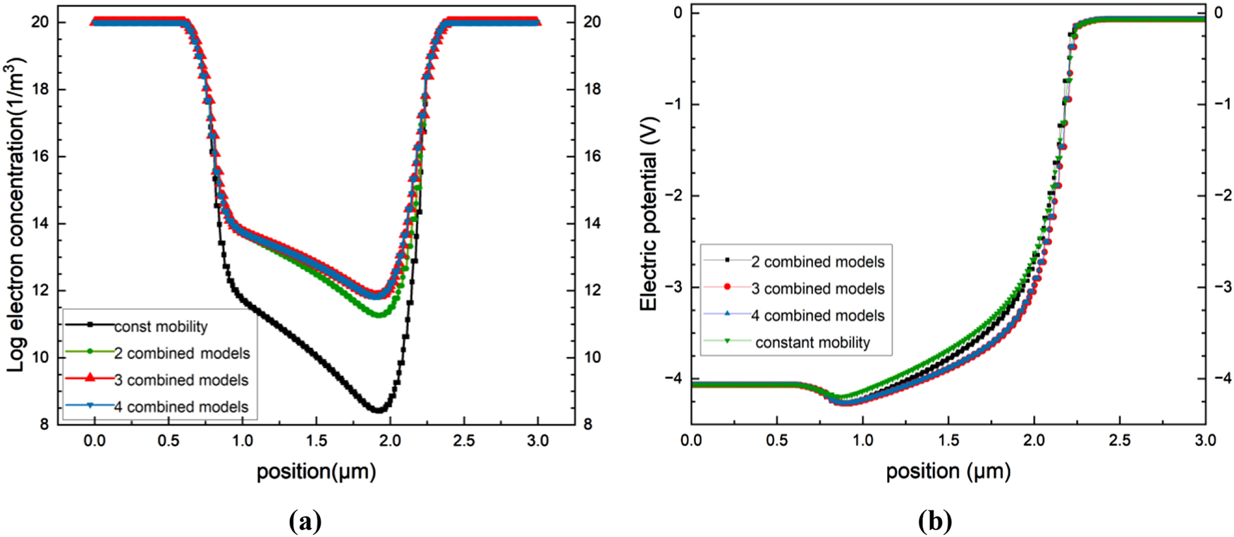
Impact of mobility modeling on carrier distribution and electrostatic behavior in the saturation regime (V g = 4 V, V d = 4 V): (a) electron concentration profile and (b) electric potential distribution along the channel.
These models account for velocity saturation effects that occur under strong electric fields. As the electric field intensity increases, carrier mobility decreases, thereby limiting the rise in current. This behavior directly affects both the potential and charge carrier distributions. In the pinch-off region near the drain, where the electric field is highest, the reduction in mobility leads to a higher carrier concentration compared to that predicted by the constant mobility model. Consequently, the pinch-off effect appears less abrupt in the field-dependent mobility models, resulting in a smoother and more physically realistic transition of carrier concentration along the channel.
5 Conclusions
This study conducted a comprehensive evaluation of various empirical mobility models to simulate silicon MOSFET behavior, emphasizing both accuracy and computational efficiency. The principal contribution lies in the systematic comparative assessment of different model integration strategies, establishing a structured framework for optimizing the trade-off between precision and computational cost in semiconductor device simulation.
Among the investigated configurations, Scenario (iii), which integrates the Fletcher model with the Arora, Lombardi, and Caughey–Thomas models to account for high-level injection effects, produced results closely matching those of Scenario (ii). Detailed analysis revealed that the relatively low injection levels under the examined operating conditions minimized the influence of the Fletcher model, rendering its additional complexity unnecessary. Consequently, Scenario (ii), which combines the Arora, Lombardi, and Caughey–Thomas models, was identified as the optimal configuration, providing accurate and reliable predictions of MOSFET behavior while maintaining superior computational efficiency.
The integration of these empirical mobility models substantially enhances the physical realism of carrier transport representation by simultaneously accounting for temperature dependence, doping concentration, and high-field mobility saturation, effects often neglected in single-model approaches. The results confirm that Scenario (ii) delivers the best balance between numerical accuracy and computational feasibility, offering a validated and practical guideline for model selection in both academic and industrial semiconductor simulation platforms.
Despite these advancements, the study acknowledges inherent limitations of classical empirical formulations. Their predictive accuracy for ultra-scaled devices (below the 20 nm technology node), where quantum confinement and tunneling effects become dominant, remains uncertain. Accordingly, future research will focus on developing hybrid quantum–empirical models that combine the validated Scenario (ii) framework with quantum correction techniques such as density-gradient theory. This hybridization will enable efficient yet physically consistent modeling of nanoscale MOSFETs, capturing critical quantum phenomena that influence inversion charge distribution, threshold voltage behavior, and subthreshold conduction.
Overall, the combined empirical mobility models proposed herein represent a significant advancement in the accurate and computationally efficient simulation of conventional and moderately scaled MOSFETs. More importantly, they establish a clear foundation for extending this methodology toward next-generation semiconductor technologies, where coupling classical transport models with quantum-mechanical corrections will be essential for predictive, high-fidelity device simulation.
Acknowledgments
Princess Nourah bint Abdulrahman University Researchers Supporting Project number (PNURSP2025R826), Princess Nourah bint Abdulrahman University, Riyadh, Saudi Arabia.
-
Funding information: Princess Nourah bint Abdulrahman University Researchers Supporting Project number (PNURSP2025R826), Princess Nourah bint Abdulrahman University, Riyadh, Saudi Arabia.
-
Author contribution: All authors have accepted responsibility for the entire content of this manuscript and approved its submission.
-
Conflict of interest: The authors state no conflict of interest.
-
Data availability statement: The datasets generated and/or analysed during the current study are available from the corresponding author on reasonable request.
Nomenclature
- A, B
-
parameters depending on the nature of the dopants
- D n , D p
-
electron and hole diffusion coefficients (m2/s)
- E
-
electric field (V/m)
- E ⊥
-
perpendicular electric field component (V/m)
- F 1
-
fletcher mobility coefficient (s2 A/(m3 kg))
- F 2
-
fletcher mobility coefficient (1/m2)
- G n
-
rate of generation and recombination of electron-hole pairs (cm−3 s−1)
- j n , j p
-
electron and hole current densities (A/m2)
- μ 0
-
electron and hole mobility reference (cm2/V s)
- μ 1, μ 2
-
model parameters for electrons and holes (cm2/V s)
- μ ccs
-
carrier-carrier scattering mobility (cm2/V s)
- μ eff
-
effective mobility (cm2/V s)
- μ I
-
impurity mobility (cm2/V s)
- μ L
-
lattice mobility (cm2/V s)
- μ n , μ p
-
electron and hole mobilities (cm2/V s)
- μ min,n
-
electron mobility minimum reference (cm2/V s)
- μ min,p
-
hole mobility minimum reference (cm2/V s)
- μ n,0, μ p,0
-
low-field electron and hole mobilities (cm2/V s)
- μ 0,n , μ 0,p
-
electron and hole mobility reference (cm2/V s)
- n, p
-
electron and hole concentrations (cm−3)
- N
-
doping concentration (cm−3)
- N 0,n
-
electron reference impurity concentration (cm−3)
- N 0,p
-
hole reference impurity concentration (cm−3)
-
-
ionized acceptor concentration (cm−3)
-
-
ionized donor concentration (cm−3)
- ϕ
-
electrostatic potential (V)
- ρ
-
charge density (C/m3)
- τ
-
relaxation time (s)
- T
-
lattice temperature (K)
- T ref
-
reference temperature (K)
- V d
-
drain voltage (V)
- V g
-
gate voltage (V)
- V th
-
threshold voltage (V)
- v n,0
-
saturation velocity for electrons (cm/s)
- v p,0
-
saturation velocity for holes (cm/s)
- α n , α p
-
material properties
- α 1,n , α 1,p
-
dimensionless model parameters
- α 2,n , α 2,p
-
dimensionless model parameters
- β n,0, β p,0
-
dimensionless model parameters
- δ
-
model parameter for electrons and holes
References
1. Bonkoungou, BDR, Gwoziecki, R, Perez, G, Sterna, L, Khatir, Z. Optimized semi-physical EKV model for simulation of SiC MOSFETs. Microelectron Reliab 2025;171:115780. https://doi.org/10.1016/j.microrel.2025.115780.Search in Google Scholar
2. Shankari, R, Supraja, G, Krushnasamy, VS, Haripriya, D, Elangovan, K. Vertical gallium nitride MOSFETs: advanced architectures, fabrication technologies, and performance breakthroughs for high-power applications. Microelectron Eng 2026;302:112418. https://doi.org/10.1016/j.mee.2025.112418.Search in Google Scholar
3. Dai, Y, Yao, J, Chen, J, Zhang, M, Xu, Y, Yao, Q, et al.. A cross-scale investigation on transient electrothermal performance for power MOSFETs at device-package level. Microelectron J 2025;156:106561. https://doi.org/10.1016/j.mejo.2025.106561.Search in Google Scholar
4. Er-rafii, H, Galadi, A. Improved temperature-scalable DC model for SiC power MOSFET including quasi-saturation effect. Solid State Electron 2024;220:108993. https://doi.org/10.1016/j.sse.2024.108993.Search in Google Scholar
5. Peng, S, Shan, H, Yang, R, Liu, Y, Deng, W. Modeling total ionizing dose radiation effects in p-type polycrystalline silicon thin film transistors. Microelectron Reliab 2025;171:115788. https://doi.org/10.1016/j.microrel.2025.115788.Search in Google Scholar
6. Shen, S, Yuan, J. Simulation of low frequency noise in buried-channel MOSFET by a Green’s function-based numerical trap level model. Solid State Electron 2022;192:108272. https://doi.org/10.1016/j.sse.2022.108272.Search in Google Scholar
7. Ding, QA, Fan, S, Ning, F, Li, J, Chen, B, Peng, Y, et al.. High-performance JLCSG MOSFET biosensor considering quantum confinement for multi-region neutral biomolecule species detection. Micro Nanostruct 2025;208:208333. https://doi.org/10.1016/j.micrna.2025.208333.Search in Google Scholar
8. Cabré, R, Muhea, WE, Iñiguez, B. Accurate semi empirical predictive model for doped and undoped double gate MOSFET. Solid State Electron 2018;149:23–31. https://doi.org/10.1016/j.sse.2018.08.003.Search in Google Scholar
9. Wong, HS. “Universal” effective mobility of empirical local mobility models for n-and p-channel silicon MOSFETs. Solid State Electron 1993;36:179–88. https://doi.org/10.1016/0038-1101(93)90137-F.Search in Google Scholar
10. Peng, B, Jiao, Y, Zhong, H, Rong, Z, Wang, Z, Xiao, Y, et al.. Compact modeling of quantum confinements in nanoscale gate-all-around MOSFETs. Fundam Res 2024;4:1306–13. https://doi.org/10.1016/j.fmre.2022.09.035.Search in Google Scholar
11. Ortiz-Conde, A, López-López, O, Gutierrez-Dominguez, E, García-Sánchez, FJ. A rigorous Fermi-Dirac statistics-based MOSFET channel surface potential equation using polylogarithms. Solid State Electron 2023;199:108507. https://doi.org/10.1016/j.sse.2022.108507.Search in Google Scholar
12. Ghosh, S. Modeling the performance of short-channel fully depleted silicon-on-insulator (SOI) metal oxide semiconductor field effect transistors (MOSFETs). In: Silicon-on-insulator (SOI) technology. Cambridge, UK: Woodhead Publishing; 2014:77–101 pp.Search in Google Scholar
13. Alessandrini, M, Esseni, D, Fiegna, C. Development of an analytical mobility model for the simulation of ultra-thin single-and double-gate SOI MOSFETs. Solid State Electron 2004;48:589–95. https://doi.org/10.1016/j.sse.2003.09.023.Search in Google Scholar
14. Ye, H, Lee, C, Raynolds, J, Haldar, P, Hennessy, MJ, Mueller, EK. Silicon power MOSFET at low temperatures: a two-dimensional computer simulation study. Cryogenics 2007;47:243–51. https://doi.org/10.1016/j.cryogenics.2007.01.007.Search in Google Scholar
15. Balaguer, M, Roldan, JB, Donetti, L, Gamiz, F. Inversion charge modeling in n-type and p-type double-gate MOSFETs including quantum effects: the role of crystallographic orientation. Solid State Electron 2012;67:30–7. https://doi.org/10.1016/j.sse.2011.09.006.Search in Google Scholar
16. Baral, K, Singh, PK, Kumar, S, Singh, AK, Jarwal, DK, Jit, S. A unified 2-D model for nanowire junctionless accumulation and inversion mode MOSFET in quasi-ballistic regime. Solid State Electron 2022;193:108282. https://doi.org/10.1016/j.sse.2022.108282.Search in Google Scholar
17. Moldovan, O, Chaves, FA, Jiménez, D, Iñiguez, B. Compact charge and capacitance modeling of undoped ultra-thin body (UTB) SOI MOSFETs. Solid State Electron 2008;52:1867–71. https://doi.org/10.1016/j.sse.2008.06.056.Search in Google Scholar
18. Roldán, JB, Gámiz, F. Simulation and modelling of transport properties in strained-Si and strained-Si/SiGe-on-insulator MOSFETs. Solid State Electron 2004;48:1347–55. https://doi.org/10.1016/j.sse.2004.01.016.Search in Google Scholar
19. Toan, HLM, Maity, SK. Physics based compact modeling of symmetric double gate MOS transistors with high mobility III–V channel material. Superlattice Microst 2021;155:106925. https://doi.org/10.1016/j.spmi.2021.106925.Search in Google Scholar
20. Palestri, P, Eminente, S, Esseni, D, Fiegna, C, Sangiorgi, E, Selmi, L. An improved semi-classical Monte-Carlo approach for nano-scale MOSFET simulation. Solid State Electron 2005;49:727–32. https://doi.org/10.1016/j.sse.2004.11.024.Search in Google Scholar
21. Madheswaran, M, Ramesh, R, Kannan, K. Hot-carrier reliability on the optical characteristics of gate stack gate all-around (GSGAA) MOSFET considering quantum mechanical effects. Optik 2016;127:2694–702. https://doi.org/10.1016/j.ijleo.2015.12.054.Search in Google Scholar
22. He, J, Xi, X, Wan, H, Dunga, M, Chan, M, Niknejad, AM. BSIM5: an advanced charge-based MOSFET model for nanoscale VLSI circuit simulation. Solid State Electron 2007;51:433–44. https://doi.org/10.1016/j.sse.2006.12.006.Search in Google Scholar
23. Bhattacherjee, S, Biswas, A. Performance analysis of long Ge channel double gate (DG) p MOSFETs with high-k gate dielectrics based on carrier concentration formulation. Microelectron Reliab 2011;51:1105–12. https://doi.org/10.1016/j.microrel.2011.02.004.Search in Google Scholar
24. Osgnach, P, Caruso, E, Lizzit, D, Palestri, P, Esseni, D, Selmi, L. The impact of interface states on the mobility and drive current of In0.53Ga0.47As semiconductor n-MOSFETs. Solid State Electron 2015;108:90–6. https://doi.org/10.1016/j.sse.2014.12.011.Search in Google Scholar
25. Cerdeira, A, Iñiguez, B, Estrada, M. Compact model for short channel symmetric doped double-gate MOSFETs. Solid State Electron 2008;52:1064–70. https://doi.org/10.1016/j.sse.2008.03.009.Search in Google Scholar
26. Wang, W, Lu, H, Song, J, Lo, SH, Taur, Y. Compact modeling of quantum effects in symmetric double-gate MOSFETs. Microelectron J 2010;41:688–92. https://doi.org/10.1016/j.mejo.2010.05.007.Search in Google Scholar
27. Fei, H, Liang, L, Zhang, Z. Investigation on temperature limitation and failure mechanism of SiC MOSFETs under avalanche conditions. Microelectron Reliab 2023;150:115106. https://doi.org/10.1016/j.microrel.2023.115106.Search in Google Scholar
28. Venugopalan, S, Lu, DD, Kawakami, Y, Lee, PM, Niknejad, AM, Hu, C. BSIM-CG: a compact model of cylindrical/surround gate MOSFET for circuit simulations. Solid State Electron 2012;67:79–89. https://doi.org/10.1016/j.sse.2011.09.001.Search in Google Scholar
29. Ratnesh, RK, Goel, A, Kaushik, G, Garg, H, Singh, M, Prasad, B, et al.. Advancement and challenges in MOSFET scaling. Mater Sci Semicond Process 2021;134:106002. https://doi.org/10.1016/j.mssp.2021.106002.Search in Google Scholar
30. Sharma, RK, Gupta, M, Gupta, RS. Two-dimensional analytical subthreshold model of graded channel DG FD SOI n-MOSFET with gate misalignment effect. Superlattice Microst 2009;45:91–104. https://doi.org/10.1016/j.spmi.2008.12.005.Search in Google Scholar
31. Sai, SB, Navaneeth, M, Kannadassan, D. Cryogenic sub-THz ultrathin-body InGaAs MOSFET: physical modeling and DC/RF analysis. J Comput Electron 2025;24:96. https://doi.org/10.1007/s10825-025-02324-3.Search in Google Scholar
32. Dastjerdy, E, Ghayour, R, Sarvari, H. 3D quantum mechanical simulation of square nanowire MOSFETs by using NEGF method. Cent Eur J Phys 2011;9:472–81. https://doi.org/10.2478/s11534-010-0097-6.Search in Google Scholar
33. Ghosh, P, Haldar, S, Gupta, RS, Gupta, M. An analytical drain current model for dual material engineered cylindrical/surrounded gate MOSFET. Microelectron J 2012;43:17–24. https://doi.org/10.1016/j.mejo.2011.10.001.Search in Google Scholar
34. Takagi, SI, Toriumi, A, Iwase, M, Tango, H. On the universality of inversion layer mobility in Si MOSFET’s: part I-effects of substrate impurity concentration. IEEE Trans Electron Dev 1994;41:2357–62. https://doi.org/10.1109/16.337449.Search in Google Scholar
35. Lee, SW. Universality of mobility-gate field characteristics of electrons in the inversion charge layer and its application in MOSFET modeling. IEEE Trans Comput Aided Des Integrated Circ Syst 1989;8:724–30. https://doi.org/10.1109/43.31529.Search in Google Scholar
36. Jeon, DS, Burk, DE. MOSFET electron inversion layer mobilities-a physically based semi-empirical model for a wide temperature range. IEEE Trans Electron Dev 1989;36:1456–63. https://doi.org/10.1109/16.30959.Search in Google Scholar
37. Chen, K, Wann, HC, Duster, J, Pramanik, D, Nariani, S, Ko, PK, et al.. An accurate semi-empirical saturation drain current model for LDD N-MOSFET. IEEE Electron Device Lett 1996;17:145–7. https://doi.org/10.1109/55.485195.Search in Google Scholar
38. Li, Q, Yang, Y, Wen, Y, Tian, X, Li, Y, Xiang, W. A fast overcurrent protection IC for SiC MOSFET based on current detection. IEEE Trans Power Electron 2024;39:4986–90. https://doi.org/10.1109/TPEL.2024.3358353.Search in Google Scholar
39. Wang, Y, Yu, CH, Li, XJ, Yang, JQ. A comparative study on heavy-ion irradiation impact on p-channel and n-channel power UMOSFETs. IEEE Trans Nucl Sci 2022;69:1249–56. https://doi.org/10.1109/TNS.2022.3175954.Search in Google Scholar
40. Sze, SM. Phys. of semiconductor devices. NY: Jhon Wiley and Sons. Inc; 1981.Search in Google Scholar
41. Pierret, RF. Semiconductor device fundamentals, 2nd ed. Reading, MA: Addison Wesley; 1996.Search in Google Scholar
42. Sze, SM, Ng, KK. Physics of semiconductor devices. Hoboken, New Jersey: John Wiley & Sons, Inc.; 2007.Search in Google Scholar
43. Streetman, BG, Banerjee, SK. Solid state electronic devices, Global Edition (7th ed.) India: Pearson Education; 2015.Search in Google Scholar
44. Diu, B, Guthmann, C, Lederer, D, Roulet, B. Physique statistique, volume 37 of Collection Enseignement des Sciences; 2001.Search in Google Scholar
45. Ashcroft, NW, Mermin, ND. Solid state. Physics. New York: Holt, Rinehart and Winston; 1976, Appendix C:1 p.Search in Google Scholar
46. Selberherr, S. Analysis and simulation of semiconductor devices. Vienna: Springer; 1984.Search in Google Scholar
47. Taur, Y, Ning, TH. Fundamentals of modern VLSI devices, 2nd ed. Cambridge: Cambridge University Press; 2009.Search in Google Scholar
48. Lundstrom, M. Fundamentals of carrier transport, 2nd ed. Measurement Science and Technology; 2002, vol 13:230 p.Search in Google Scholar
49. Orton, JW. The story of semiconductors. Oxford: OUP; 2008.Search in Google Scholar
50. Ferry, D. Semiconductor transport, 1st ed. London: CRC Press; 2000.Search in Google Scholar
51. Datta, S. Quantum transport: atom to transistor. Cambridge, UK: Cambridge University Press; 2005.Search in Google Scholar
52. Jacoboni, C, Canali, C, Ottaviani, G, Quaranta, AA. A review of some charge transport properties of silicon. Solid State Electron 1977;20:77–89. https://doi.org/10.1016/0038-1101(77)90054-5.Search in Google Scholar
53. Chen, K, Wann, HC, Dunster, J, Ko, PK, Hu, C, Yoshida, M. MOSFET carrier mobility model based on gate oxide thickness, threshold and gate voltages. Solid State Electron 1996;39:1515–18. https://doi.org/10.1016/0038-1101(96)00059-7.Search in Google Scholar
54. Sah, CT, Ning, TH, Tschopp, LL. The scattering of electrons by surface oxide charges and by lattice vibrations at the silicon-silicon dioxide interface. Surf Sci 1972;32:561–75. https://doi.org/10.1016/0039-6028(72)90183-5.Search in Google Scholar
55. Schroder, DK. Advanced MOS devices. Reading, Mass: Addison-Wesley Pub. Co.; 1987. Available from: https://lccn.loc.gov/85028585.Search in Google Scholar
56. Caughey, DM, Thomas, RE. Carrier mobilities in silicon empirically related to doping and field. Proc IEEE 1967;55:2192–3. https://doi.org/10.1109/PROC.1967.6123.Search in Google Scholar
57. Arora, ND, Hauser, JR, Roulston, DJ. Electron and hole mobilities in silicon as a function of concentration and temperature. IEEE Trans Electron Dev 1982;29:292–5. https://doi.org/10.1109/T-ED.1982.20698.Search in Google Scholar
58. Lombardi, C, Manzini, S, Saporito, A, Vanzi, M. A physically based mobility model for numerical simulation of nonplanar devices. IEEE Trans Comput Aided Des Integrated Circ Syst 1988;7:1164–71. https://doi.org/10.1109/43.9186.Search in Google Scholar
59. Dorkel, JM, Leturcq, P. Carrier mobilities in silicon semi-empirically related to temperature, doping and injection level. Solid State Electron 1981;24:821–5. https://doi.org/10.1016/0038-1101(81)90097-6.Search in Google Scholar
60. Fletcher, NH. The high current limit for semiconductor junction devices. Proc IRE 1957;45:862–72. https://doi.org/10.1109/JRPROC.1957.278485.Search in Google Scholar
© 2025 the author(s), published by De Gruyter, Berlin/Boston
This work is licensed under the Creative Commons Attribution 4.0 International License.
Articles in the same Issue
- Research Articles
- Single-step fabrication of Ag2S/poly-2-mercaptoaniline nanoribbon photocathodes for green hydrogen generation from artificial and natural red-sea water
- Abundant new interaction solutions and nonlinear dynamics for the (3+1)-dimensional Hirota–Satsuma–Ito-like equation
- A novel gold and SiO2 material based planar 5-element high HPBW end-fire antenna array for 300 GHz applications
- 10.1515/phys-2024-0117
- 10.1515/phys-2024-0119
- Numerical study of flow and heat transfer in the air-side metal foam partially filled channels of panel-type radiator under forced convection
- Water-based hybrid nanofluid flow containing CNT nanoparticles over an extending surface with velocity slips, thermal convective, and zero-mass flux conditions
- Dynamical wave structures for some diffusion--reaction equations with quadratic and quartic nonlinearities
- 10.1515/phys-2025-0120
- 10.1515/phys-2024-0108
- Influence of Hall current and acoustic pressure on nanostructured DPL thermoelastic plates under ramp heating in a double-temperature model
- Applications of the Belousov–Zhabotinsky reaction–diffusion system: Analytical and numerical approaches
- AC electroosmotic flow of Maxwell fluid in a pH-regulated parallel-plate silica nanochannel
- 10.1515/phys-2025-0127
- Modeling and analysis of quantum communication channel in airborne platforms with boundary layer effects
- Theoretical and numerical investigation of a memristor system with a piecewise memductance under fractal–fractional derivatives
- Tuning the structure and electro-optical properties of α-Cr2O3 films by heat treatment/La doping for optoelectronic applications
- High-speed multi-spectral explosion temperature measurement using golden-section accelerated Pearson correlation algorithm
- 10.1515/phys-2025-0144
- Study on the duration of laser-induced air plasma flash near thin film surface
- Exploring the dynamics of fractional-order nonlinear dispersive wave system through homotopy technique
- 10.1515/phys-2025-0135
- 10.1515/phys-2025-0137
- Numerical examination of the chemically reactive MHD flow of hybrid nanofluids over a two-dimensional stretching surface with the Cattaneo–Christov model and slip conditions
- 10.1515/phys-2025-0142
- Stability analysis of unsteady ternary nanofluid flow past a stretching/shrinking wedge
- 10.1515/phys-2025-0150
- Bilinear form and soltion solutions for (3+1)-dimensional negative-order KdV-CBS equation
- Solitary chirp pulses and soliton control for variable coefficients cubic–quintic nonlinear Schrödinger equation in nonuniform management system
- 10.1515/phys-2025-0145
- Dissipative disorder optimization in the radiative thin film flow of partially ionized non-Newtonian hybrid nanofluid with second-order slip condition
- Bifurcation, chaotic behavior, and traveling wave solutions for the fractional (4+1)-dimensional Davey–Stewartson–Kadomtsev–Petviashvili model
- New investigation on soliton solutions of two nonlinear PDEs in mathematical physics with a dynamical property: Bifurcation analysis
- Mathematical analysis of nanoparticle type and volume fraction on heat transfer efficiency of nanofluids
- Creation of single-wing Lorenz-like attractors via a ten-ninths-degree term
- Optical soliton solutions, bifurcation analysis, chaotic behaviors of nonlinear Schrödinger equation and modulation instability in optical fiber
- Chaotic dynamics and some solutions for the (n + 1)-dimensional modified Zakharov–Kuznetsov equation in plasma physics
- Fractal formation and chaotic soliton phenomena in nonlinear conformable Heisenberg ferromagnetic spin chain equation
- 10.1515/phys-2025-0132
- 10.1515/phys-2025-0124
- Tavis–Cummings model in the presence of a deformed field and time-dependent coupling
- Spinning dynamics of stress-dependent viscosity of generalized Cross-nonlinear materials affected by gravitationally swirling disk
- Design and prediction of high optical density photovoltaic polymers using machine learning-DFT studies
- 10.1515/phys-2025-0178
- Coating thickness and process efficiency of reverse roll coating using a magnetized hybrid nanomaterial flow
- Dynamic analysis, circuit realization, and its synchronization of a new chaotic hyperjerk system
- Decoherence of steerability and coherence dynamics induced by nonlinear qubit–cavity interactions
- 10.1515/phys-2025-0174
- Modulational instability and associated ion-acoustic modulated envelope solitons in a quantum plasma having ion beams
- Statistical inference of constant-stress partially accelerated life tests under type II generalized hybrid censored data from Burr III distribution
- 10.1515/phys-2025-0185
- Entropy optimization for chemically reactive magnetized unsteady thin film hybrid nanofluid flow on inclined surface subject to nonlinear mixed convection and variable temperature
- 10.1515/phys-2025-0179
- 10.1515/phys-2025-0190
- Novel analysis of fractional regularized long-wave equation in plasma dynamics
- Development of a photoelectrode based on a bismuth(iii) oxyiodide/intercalated iodide-poly(1H-pyrrole) rough spherical nanocomposite for green hydrogen generation
- Investigation of solar radiation effects on the energy performance of the (Al2O3–CuO–Cu)/H2O ternary nanofluidic system through a convectively heated cylinder
- Quantum resources for a system of two atoms interacting with a deformed field in the presence of intensity-dependent coupling
- Studying bifurcations and chaotic dynamics in the generalized hyperelastic-rod wave equation through Hamiltonian mechanics
- A new numerical technique for the solution of time-fractional nonlinear Klein–Gordon equation involving Atangana–Baleanu derivative using cubic B-spline functions
- Interaction solutions of high-order breathers and lumps for a (3+1)-dimensional conformable fractional potential-YTSF-like model
- 10.1515/phys-2025-0192
- 10.1515/phys-2025-0188
- Numerical investigation of mixed convection and viscous dissipation in couple stress nanofluid flow: A merged Adomian decomposition method and Mohand transform
- Effectual quintic B-spline functions for solving the time fractional coupled Boussinesq–Burgers equation arising in shallow water waves
- Analysis of MHD hybrid nanofluid flow over cone and wedge with exponential and thermal heat source and activation energy
- Solitons and travelling waves structure for M-fractional Kairat-II equation using three explicit methods
- Impact of nanoparticle shapes on the heat transfer properties of Cu and CuO nanofluids flowing over a stretching surface with slip effects: A computational study
- Computational simulation of heat transfer and nanofluid flow for two-sided lid-driven square cavity under the influence of magnetic field
- 10.1515/phys-2025-0200
- 10.1515/phys-2025-0199
- Exploring the peakon solitons molecules and solitary wave structure to the nonlinear damped Kortewege–de Vries equation through efficient technique
- Modeling and heat transfer analysis of magnetized hybrid micropolar blood-based nanofluid flow in Darcy–Forchheimer porous stenosis narrow arteries
- Activation energy and cross-diffusion effects on 3D rotating nanofluid flow in a Darcy–Forchheimer porous medium with radiation and convective heating
- 10.1515/phys-2025-0201
- Influence of a magnetic field on double-porosity photo-thermoelastic materials under Lord–Shulman theory
- 10.1515/phys-2025-0189
- Analytical and numerical investigation of exact wave patterns and chaotic dynamics in the extended improved Boussinesq equation
- Nonclassical correlation dynamics of Heisenberg XYZ states with (x, y)-spin--orbit interaction, x-magnetic field, and intrinsic decoherence effects
- Exact traveling wave and soliton solutions for chemotaxis model and (3+1)-dimensional Boiti–Leon–Manna–Pempinelli equation
- Unveiling the transformative role of samarium in ZnO: Exploring structural and optical modifications for advanced functional applications
- On the derivation of solitary wave solutions for the time-fractional Rosenau equation through two analytical techniques
- 10.1515/phys-2025-0160
- Advanced mathematical analysis of heat and mass transfer in oscillatory micropolar bio-nanofluid flows via peristaltic waves and electroosmotic effects
- 10.1515/phys-2025-0211
- Some anisotropic and perfect fluid plane symmetric solutions of Einstein's field equations using killing symmetries
- Nonlinear dynamics of the dissipative ion-acoustic solitary waves in anisotropic rotating magnetoplasmas
- Curves in multiplicative equiaffine plane
- Exact solution of the three-dimensional (3D) Z2 lattice gauge theory
- 10.1515/phys-2025-0210
- Symbolic computation: Analytical solutions and dynamics of a shallow water wave equation in coastal engineering
- Wave propagation in nonlocal piezo-photo-hygrothermoelastic semiconductors subjected to heat and moisture flux
- Comparative reaction dynamics in rotating nanofluid systems: Quartic and cubic kinetics under MHD influence
- Laplace transform technique and probabilistic analysis-based hypothesis testing in medical and engineering applications
- Physical properties of ternary chloro-perovskites KTCl3 (T = Ge, Al) for optoelectronic applications
- Gravitational length stretching: Curvature-induced modulation of quantum probability densities
- The search for the cosmological cold dark matter axion – A new refined narrow mass window and detection scheme
- A comparative study of quantum resources in bipartite Lipkin–Meshkov–Glick model under DM interaction and Zeeman splitting
- 10.1515/phys-2025-0233
- Nanospherical arsenic(iii) oxoiodide/iodide-intercalated poly(N-methylpyrrole) composite synthesis for broad-spectrum optical detection
- Sine power Burr X distribution with estimation and applications in physics and other fields
- 10.1515/phys-2025-0197
- Dynamical analyses and dispersive soliton solutions to the nonlinear fractional model in stratified fluids
- Computation of exact analytical soliton solutions and their dynamics in advanced optical system
- An innovative approximation concerning the diffusion and electrical conductivity tensor at critical altitudes within the F-region of ionospheric plasma at low latitudes
- An analytical investigation to the (3+1)-dimensional Yu–Toda–Sassa–Fukuyama equation with dynamical analysis: Bifurcation
- 10.1515/phys-2025-0234
- Numerical analysis of non-similar convection flows of a two-phase nanofluid past a semi-infinite vertical plate with thermal radiation
- MgO NPs reinforced PCL/PVC nanocomposite films with enhanced UV shielding and thermal stability for packaging applications
- Optimal conditions for indoor air purification using non-thermal Corona discharge electrostatic precipitator
- 10.1515/phys-2025-0230
- Tunable double plasmon-induced transparency based on monolayer patterned graphene metamaterial
- DSC: depth data quality optimization framework for RGBD camouflaged object detection
- 10.1515/phys-2025-0241
- Numerical investigation of couple stress under slip conditions via modified Adomian decomposition method
- Monitoring plateau lake area changes in Yunnan province, southwestern China using medium-resolution remote sensing imagery: applicability of water indices and environmental dependencies
- Heterodyne interferometric fiber-optic gyroscope
- Exact solutions of Einstein’s field equations via homothetic symmetries of non-static plane symmetric spacetime
- 10.1515/phys-2025-0231
- Empirical model integration for accurate charge carrier mobility simulation in silicon MOSFETs
- 10.1515/phys-2025-0245
- 10.1515/phys-2025-0250
- 10.1515/phys-2025-0253
- Analysis of iterative deblurring: no explicit noise
- 10.1515/phys-2025-0251
- Review Article
- Examination of the gamma radiation shielding properties of different clay and sand materials in the Adrar region
- Erratum
- Erratum to “On Soliton structures in optical fiber communications with Kundu–Mukherjee–Naskar model (Open Physics 2021;19:679–682)”
- Special Issue on Fundamental Physics from Atoms to Cosmos - Part II
- Possible explanation for the neutron lifetime puzzle
- Special Issue on Nanomaterial utilization and structural optimization - Part III
- Numerical investigation on fluid-thermal-electric performance of a thermoelectric-integrated helically coiled tube heat exchanger for coal mine air cooling
- Special Issue on Nonlinear Dynamics and Chaos in Physical Systems
- Analysis of the fractional relativistic isothermal gas sphere with application to neutron stars
- Abundant wave symmetries in the (3+1)-dimensional Chafee–Infante equation through the Hirota bilinear transformation technique
- Successive midpoint method for fractional differential equations with nonlocal kernels: Error analysis, stability, and applications
- 10.1515/phys-2025-0214