
Nanospherical arsenic(iii) oxoiodide/iodide-intercalated poly(N-methylpyrrole) composite synthesis for broad-spectrum optical detection
-
Fatemah H. Alkallas
 und
Mohamed Rabia
und
Mohamed Rabia

Abstract
This study presents the successful synthesis of an innovative nanospherical As(iii) oxoiodide/iodide-intercalated poly(N-methylpyrrole) composite (As(iii)OI/I-PNMP NS composite), which serves as an n-type active layer in a high-performance photodetector. The composite is coated onto a polypyrrole (PPy) base, creating a novel As(iii)OI/I-PNMP/PPy heterojunction device that efficiently senses photons. Structural analysis of the synthesized composite shows uniformly distributed spherical nanoparticles, averaging around 100 nm in diameter, on a rough, highly textured surface that improves light–matter interaction. It exhibits a promising crystallite size of 21 nm and an optimal bandgap of 2.35 eV, facilitating effective absorption across a broad spectral range. The optoelectronic performance of the photodetector was systematically tested under varying illumination conditions, employing photons from both UV and visible (Vis) regions. During illumination, the photoresponse was analyzed using current density measurements (J ph), highlighting the composite’s essential role in charge carrier generation and transport. The device’s photoresponsivity (R) was notably improved, achieving values between 0.23 and 0.28 mA/W, reflecting the material’s high sensitivity to incoming light. Furthermore, the detectivity (D), an important performance metric for photodetectors, was calculated to be between 0.52 × 10⁸ and 0.63 × 10⁸ Jones, indicating excellent proficiency in detecting low-intensity optical signals. In summary, incorporating As(iii)OI with I-doped PNMP into a PPy-based structure signifies a promising strategy for developing broadband, high-efficiency photodetectors, with significant potential for future use in optoelectronic sensing and imaging technologies.
1 Introduction
Optoelectronic devices are essential in various advanced technological systems, especially in the aerospace and aviation sectors [1,2]. The fundamental function of these systems is to transform light energy into electrical signals, achieved through the creation of electron-hole pairs when light is absorbed. This process of charge carrier generation is essential for their ability to detect and react to light stimuli with exceptional sensitivity and accuracy. The ongoing advancement of optoelectronic systems depends on discovering and designing materials that enhance photoresponsivity, boost charge separation efficiency, and function reliably under diverse environmental conditions [3].
N-Type semiconductors are widely studied for optoelectronic applications, as they offer excellent optical transparency, adjustable energy band gaps, and reliable electronic performance. Tin oxide (SnO) and phenyl-C61-butyric acid methyl ester (PCBM) are notable examples of n-type semiconductors with favorable characteristics [4]. These materials effectively transport electrons, making them suitable for electron-conducting layers in photodetectors and solar cells. However, a significant drawback of many n-type materials is their comparatively low charge carrier mobility, which can hinder the efficiency of photo-generated charge transport, particularly during high-frequency operation or low-intensity lighting. This limitation has spurred ongoing research focused on discovering or engineering new n-type materials or composites that provide enhanced electron mobility while preserving their advantageous optical properties [5].
Conversely, p-type semiconductors that primarily conduct through holes are crucial in optoelectronic device design. Copper oxide (CuO), a well-researched p-type metal oxide, is recognized for its ability to produce significant photocurrents, thanks to the effective movement of holes opposite to that of electrons [6,7]. This behavior enhances charge separation and collection, boosting the device’s overall performance. Similar to n-type materials, the performance of p-type materials is significantly impacted by their bandgap, which determines the range of wavelengths they can absorb. Bandgap engineering, often realized through nanostructuring or the creation of composites, enables the customization of materials’ optical responses to fit specific application needs. Additionally, crystal structure, phase purity, and nanoscale morphology influence the bandgap and optoelectronic performance.
While n-type and p-type semiconductors hold great potential, their restricted photoresponsivity is a significant hurdle in creating efficient photodetectors (R). This parameter, the ratio of photocurrent to incident light power, indicates how sensitive a material is to light. Although many materials have suitable band gaps, they often experience recombination losses or inadequate interfacial charge transport, resulting in relatively low photoresponsivity. Consequently, there is a growing focus on engineering innovative composite materials that merge the advantages of n-type and p-type components while addressing their shortcomings [1,8]. Also, photodetectors based on Si materials may achieve broader optical absorbance; however, they suffer from several drawbacks, including instability at high temperatures, the use of highly complex synthesis techniques, and high production costs [9,10].
Previous research has explored various materials and composite systems to enhance the performance of photodetectors. For example, silicon-based heterojunctions, including CuO/Si [9], have been investigated, providing reasonable structural compatibility yet limited sensitivity. Likewise, metal oxide heterostructures, such as ZnO/Cu2O [10] and graphene oxide/Cu2O [11], have shown photoresponsivity values near 0.005 mA/W. While these values are measurable, they fall short for high-performance applications. Additionally, some researchers are focusing on carbon-based materials like PC₇₁BM [12] and conductive polymer hybrids, including TiO2-polyaniline (PANI) composites [13], intending to improve both flexibility and functionality.
Conductive polymers have recently become a highly appealing category of materials for optoelectronic applications, thanks to their distinctive blend of mechanical flexibility, adjustable electrical conductivity, and ease of processing [11,12]. These organic semiconductors provide several benefits compared to inorganic ones, such as cost-effective manufacturing, durability in various environments, and suitability for flexible substrates. In particular, PNMP emerges as a highly promising option for photodetector applications. PNMP possesses a conjugated backbone that enables efficient charge delocalization, leading to better light absorption and movement of charge carriers. Its environmentally friendly characteristics and straightforward synthesis make it attractive for large-scale device production.
This study examines how the optical performance of PNMP can be further improved by incorporating inorganic nanoparticles, particularly metal oxides like arsenic iodide (As(iii)OI). These nanocomposites often show synergistic effects due to the interfacial interactions between the organic polymer and the inorganic phase. Such interactions can enhance crystallinity, charge mobility, and light-harvesting capabilities. When PNMP is paired with materials such as As(iii)OI, the resulting composite displays superior optical absorption, a broader spectral response, and a reduced bandgap, making it more suitable for optoelectronic applications. These hybrid nanocomposites capitalize on the strengths of organic and inorganic components and offer a platform for bandgap tuning and interface engineering, which are vital for optimizing photodetector performance. Developing such materials represents a proactive approach in optoelectronics, aiming to address current limitations and satisfy the increasing demand for high-sensitivity, low-power, and cost-effective photodetection technologies. In our device design, the photodetection process is inherently synchronized with the incident light modulation to ensure accurate and reproducible measurements across the targeted broadband range. The synchronization is achieved by coordinating the illumination source and the electrical readout system, such that the photocurrent response is recorded in real time. We construct a functional heterojunction capable of efficient charge separation and light-induced current generation by integrating the n-type As(iii)OI/I-PNMP nanocomposite with p-type polypyrrole (PPy). By maintaining precise timing between optical excitation and electrical measurement, the device performance metrics – particularly responsivity and detectivity – are accurately extracted, thereby validating the broadband detection capability. This work highlights the potential of combining conductive polymers with metal oxide nanoparticles to develop next-generation optoelectronic devices with improved responsivity and stability.
2 Experimental section
2.1 Materials and characteristics
N-methylpyrrole (99.9% purity) was procured from Sigma-Aldrich, Germany. In addition, several crucial reagents were acquired from Pio-Chem, Egypt, including ammonium persulfate ((NH4)2S2O8, 99.9%), potassium iodide (KI, 99.9%), iodine (I2, 99.9%), and acetic acid (CH3COOH, 99.8%). Moreover, sodium arsenite (NaAsO2, 99.9%) and hydrochloric acid (HCl, 36%) were supplied by VWR, Germany, ensuring their high purity and reliability.
The characterization methods employed in this study comprise X-ray diffraction (XRD) (X-Pert) for the determination of crystalline phases, fourier transform infrared spectroscopy (FTIR) (Bruker) for the analysis of molecular vibrations, UV-Vis spectroscopy (PerkinElmer) for the examination of electronic transitions, X-ray photoelectron spectroscopy (XPS) (Kratos) for the assessment of surface chemical composition, in addition to both transmission electron microscopy (TEM) (JEOL) and SEM (Zeiss) for a comprehensive analysis of microstructural and morphological features investigations.
2.2 Fabrication of the As(iii)OI/I-PNMP/PPy photodetector device
The As(iii)OI/I-PNMP/PPy photodetector is developed using a two-step method that involves depositing two separate layers: the p-type polypyrrole (PPy), produced following our previously documented technique [13], and the n-type As(iii)OI/I-PNMP composite layer (Figure 1(a)).
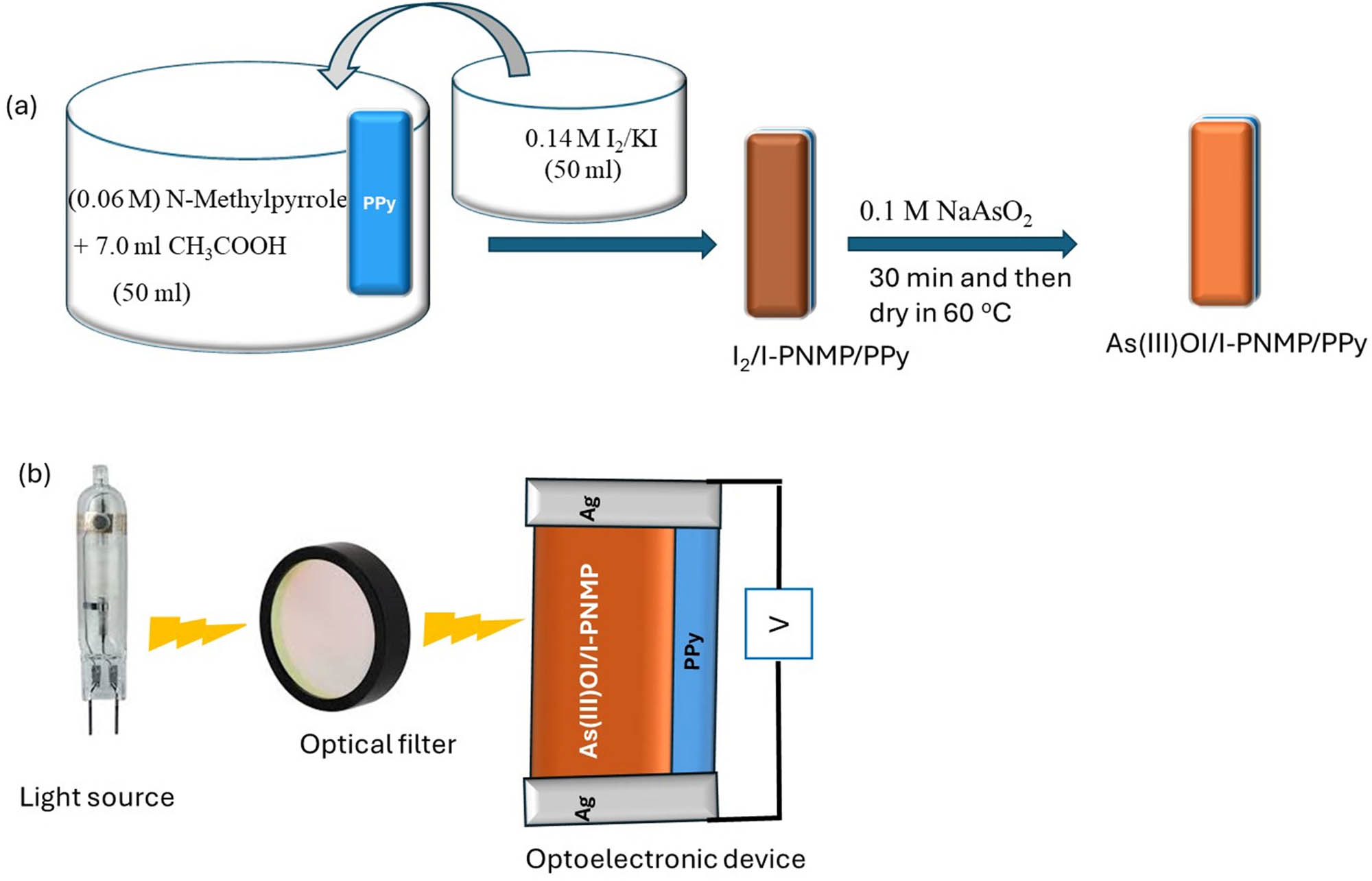
(a) Schematic illustration of the fabrication process and (b) electrical performance testing of the As(iii)OI/I-PNMP/PPy-based device.
The n-layer fabrication incorporates highly light-sensitive materials, particularly the As(iii)OI/I-PNMP NS-composite, into the PPy layer. This composite is developed through a meticulously controlled oxidation and doping procedure to improve its optoelectronic characteristics. The process starts with the oxidation of the N-methylpyrrole monomer (0.06 M) using iodine (0.14 M) as the oxidizing agent. In this reaction, the N-methylpyrrole monomer is dissolved in 7 mL of acetic acid to ensure it disperses properly in the medium. Simultaneously, iodine (I2) is dissolved using solid potassium iodide (KI), which helps release iodide ions into the system. As the oxidation progresses, iodine reacts with the monomer, triggering polymerization. This reaction results in a polymer network that incorporates iodide ions, forming the I2/I-PNMP complex material.
Following initial polymerization, doping the polymer with arsenic ions is the next important step. This occurs via the reaction of the pre-formed I2/I-PNMP complex with sodium arsenite (NaAsO2, 0.1 M). During this phase, arsenic ions (As(iii)) are successfully integrated into the polymer network, creating the As(iii)OI/I-PNMP NS-composite. Ultimately, this composite is deposited as a thin film on a glass substrate to ensure even coverage and optimal interaction with incident light. The resulting photodetector device is engineered to provide heightened sensitivity and efficiency to light exposure, making it ideal for advanced optoelectronic applications.
2.3 Electrical testing of the As(iii)OI/I-PNMP/PPy photodetector device
The electrical characterization of the As(iii)OI/I-PNMP/PPy photodetector is performed to evaluate its performance when illuminated by light. This assessment primarily aims to analyze the generation and migration of hot electrons from the photodetector’s surface under light exposure, serving as a crucial indicator of its efficiency and sensitivity.
To achieve this, a CHI workstation is employed, utilizing linear sweep voltammetry to assess the photodetector’s current density (J ph). Two silver (Ag) contacts are positioned at opposite edges of the thin film to establish the electrical connection between the photodetector and the composite film. The active surface area of the device is about 1.0 cm², which facilitates a consistent and controlled assessment of the electrical response. A vacuum metal halide lamp (100 mW/cm−2), China, illuminates the photodetector, emitting broad-spectrum white light to enable thorough testing across various photon energies. When light hits the photodetector surface, the response is captured as J ph, signifying the photocurrent density. Additionally, the dark current density (J o) is recorded without illumination to establish a baseline for comparison. This comparison aids in understanding the degree of enhancement in electrical conductivity when exposed to light. The J ph value is calculated across different photon frequencies to evaluate the photodetector’s performance further. This analysis reveals how the photodetector responds to various light wavelengths, showcasing its spectral sensitivity. By graphing the photocurrent response against different photon energies, the photodetector’s adaptability within the electromagnetic spectrum can be examined (Figure 1(b)). The estimated optical filters (730, 540, 440, and 340 nm) are supported by Thorlabs Inc., USA.
Two essential performance metrics, photoresponsivity (R) and detectivity (D), are calculated to assess the efficiency of the photodetector. The photoresponsivity (R) is derived from Eq. (1) [2,17], which incorporates the relationship between J ph, incident light power density (P), and the active surface area (S). Likewise, detectivity (D) is obtained using Eq. (2) [2,17], taking into account J ph, background noise, and electron charge (e). These metrics offer an in-depth insight into the photodetector’s capacity to detect and respond to incoming photons effectively. By performing these electrical tests, the performance and sensitivity of the As(iii)OI/I-PNMP NS-composite photodetector can be thoroughly assessed, aiding its prospective applications in advanced optoelectronics.
3 Results and discussion
3.1 Physicochemical analysis of the synthesized NS-composite
Figure 2(a) showcases the FTIR spectra of the As(iii)OI/I-PNMP composite (red) compared to the I2/I-PNMP system (black), highlighting vibrational modes that indicate successful structural and chemical interactions within the composite matrix. The I2/I-PNMP spectrum reveals characteristic absorption bands at 886, 1,051, 1,142, and 1,404 cm⁻¹, attributable to out-of-plane bending vibrations and C═C stretching associated with substituted aromatic amine structures. The bands observed around 1,311 and 3,409 cm⁻¹ correspond to C–N stretching and N–H stretching vibrations [18], signifying the integrity of the PNMP polymer backbone and its amine functionalities. These characteristics represent the fundamental vibrational profile of the iodine-doped polymer system. Upon incorporating as (iii)OI into the I-PNMP matrix, distinct spectral changes manifest in the composite spectrum. Notably, the absorption band at 1,051 cm⁻¹ shows a slight shift and a significant decrease in intensity. This indicates interaction or coordination between the arsenic species and the electron-donating groups (likely nitrogen or oxygen atoms) of the PNMP chains. Additionally, a new, prominent band at 1,529 cm⁻¹ appears solely in the composite, likely corresponding to As–O stretching or asymmetric vibrational modes, further validating the successful integration of arsenic oxide species. In the higher wavenumber region (3,000–3,500 cm⁻1), subtle shifts in N–H stretching vibrations are noted – from 3,409 cm⁻1 in I2/I-PNMP to 3,411 cm⁻1 in the composite – along with the emergence of a new band at 3,128 cm⁻¹ [19]. These alterations suggest potential hydrogen bonding or coordination between the PNMP matrix and hydroxyl/oxide groups derived from As(iii)OI. These spectral modifications provide compelling evidence for the chemical integration of As(iii)OI within the I2/I-PNMP framework, enhancing the material’s structural complexity and potential functional capabilities in catalytic or adsorption applications. A distinct spectral feature appears at 885 cm⁻¹, where the band intensity shows a significant reduction after the composite is formed. This reduction arises from the incorporation of the inorganic As(iii)OI phase into the polymer framework, which modifies the local vibrational environment associated with this mode. Similar shifts and intensity changes in low-wavenumber bands have also been reported in previous studies [14,15].
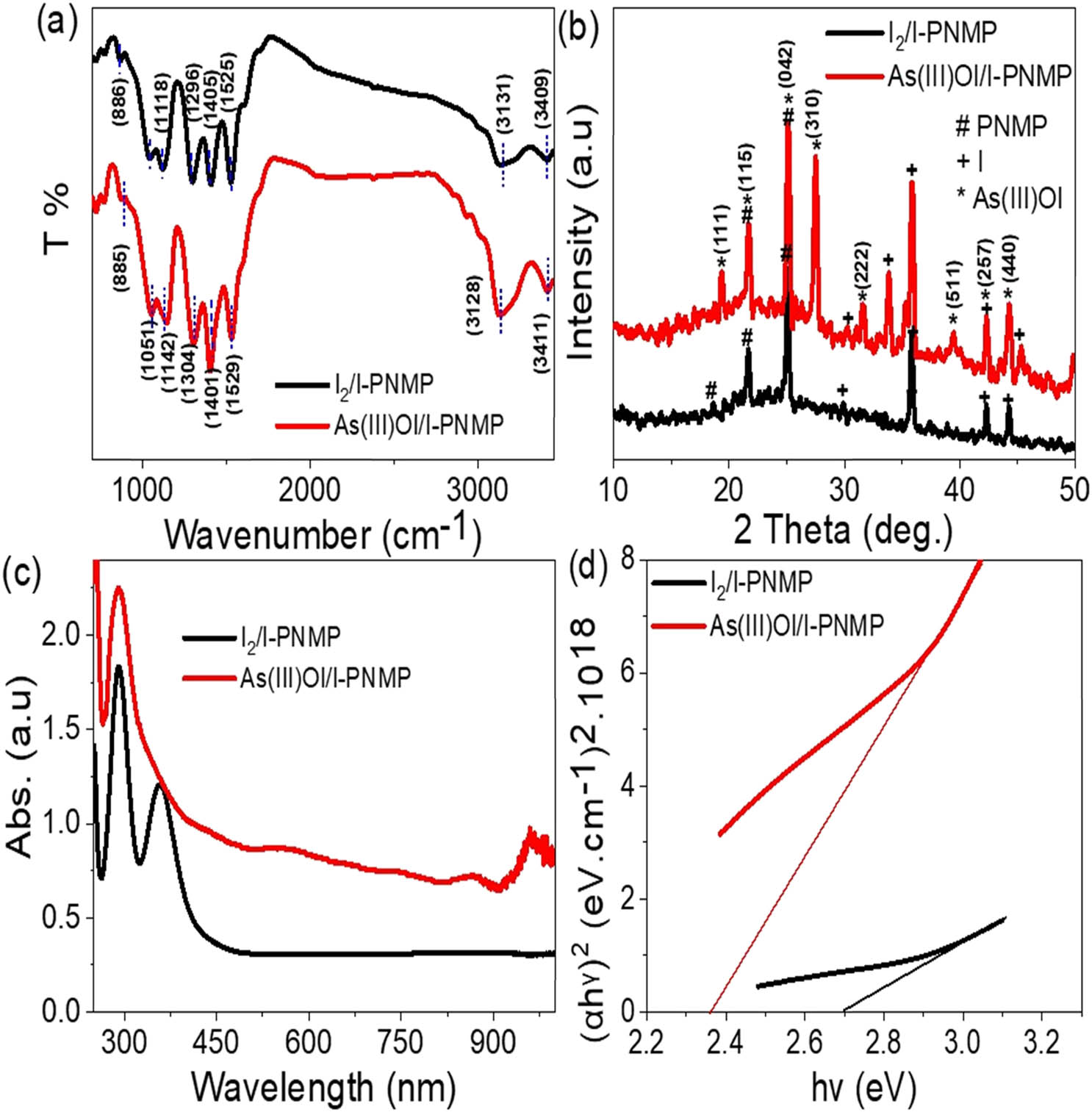
Chemical and optical characterization of the As(iii)OI/I-PNMP composite: (a) FTIR spectrum and (b) XRD pattern illustrate the structural and compositional features, while (c) UV–Vis absorption spectrum and (d) Tauc plot provide insights into the optical absorbance behavior and bandgap estimation, respectively.
The synthesized As(iii)OI/I-PNMP NS-composite’s structural and physicochemical properties were extensively analyzed through XRD, as shown in Figure 2(b). The XRD pattern reveals essential information about the material’s crystallinity and phase composition. Notably, there is a significant increase in the XRD intensity of the As(iii)OI/I-PNMP NS composite compared to the I2/I-PNMP complex, indicating improved optical behavior. This suggests that the material has a heightened capacity for photon absorption, which is vital for its use in photoactive devices.
Upon exposure to light, the absorbed photons transfer their energy to free electrons, elevating them into an excited state characterized by increased kinetic energy. This energy transfer mechanism is fundamental to the material’s photoresponsivity, thus significantly influencing its sensitivity to incident light. The crystalline characteristics of As(iii)OI/I-PNMP NS composite are further validated by identifying distinct diffraction peaks, which confirm the presence of various crystal planes.
In the case of the As(iii)OI phase, a total of eight diffraction peaks were observed at 2θ values of 19.3° (corresponding to the (111) plane), 21.7° ((115) plane), 25.1° ((042) plane), 27.5° ((310) plane), 31.6° ((222) plane), 39.4° ((511) plane), 42.3° ((257) plane), and 44.3° ((444) plane), as referenced in JCPDS card 23-1519 [20]. Similarly, the iodide phase displayed prominent peaks at 30.4°, 33.4°, 36.0°, 42.3°, and 45.3°, thus confirming the integration of iodide within the composite matrix [21]. The PNMP polymer indicated diffraction peaks at 21.7° and 25.1°, signifying its structural contribution to the hybrid composite. The presence of both iodide and PNMP in the synthesized material was further substantiated by comparison with the I2/I-PNMP complex, thereby ensuring the successful formation of the targeted NS composite.
The size of the crystallites in the As(iii)OI/I-PNMP NS-composite was determined using Equation (3) [16,17], which accounts for the incident X-ray wavelength and the full-width at half maximum (FWHM) of the diffraction peaks. The calculated crystallite size was roughly 21 nm, highlighting its nanostructured characteristics.
This nanoscale dimension is crucial for boosting the material’s photon absorption ability. The small crystallite size enables the formation of a strong localized electric field, which promotes the efficient generation and transport of hot electrons. These high-energy charge carriers demonstrate the composite’s capacity to transform incoming light into usable electrical signals, emphasizing its potential for applications in optoelectronics and photodetection. Thus, the XRD analysis verifies the well-defined crystallinity and nanoscale attributes of the synthesized As(iii)OI/I-PNMP NS composite, positioning it as a promising candidate for advanced photoactive and semiconductor-related technologies.
The optical attributes of the As(iii)OI/I-PNMP nanostructured composite (NS-composite) were thoroughly examined with UV–Vis absorption spectroscopy, depicted in Figure 2(c). The Tauc plot analysis presented in Figure 2(d) obtained the corresponding optical bandgap values. A notable link between the absorption spectrum and bandgap estimation underscores the composite material’s adequate light-harvesting capacity.
The absorption spectrum of the As(iii)OI/I-PNMP composite shows a notable redshift compared to the pristine PNMP polymer. This composite feature has a strong, broad absorption that reaches up to about 520 nm, while the PNMP polymer’s absorption edge caps at approximately 450 nm. The broader absorption spectrum of the composite suggests enhanced optical performance, likely due to the synergistic interactions between the inorganic arsenic oxide and the conjugated PNMP matrix. These interactions may promote charge transfer processes and improve the material’s light absorption capacity. Furthermore, the Tauc method (Eq. (4)) [18,19] was utilized to estimate optical band gap values, assuming an indirect electronic transition with a power factor of n = 1/2, following Eq. (4). The band gap for the As(iii)OI/I-PNMP composite was approximately 2.35 eV, significantly lower than the 2.7 eV estimated for pristine PNMP. This decrease in band gap energy aligns with the observed increase in visible light absorption and indicates enhanced semiconducting behavior. Altogether, the shift in the absorption edge and the reduction in band gap upon incorporating As(iii)OI into the PNMP matrix demonstrate improved optical activity. These features position the composite as a strong candidate for optoelectronics, photocatalysis, or solar energy applications, where efficient light absorption and charge transfer are essential.
Accurately identifying the oxidation states of key elements – arsenic (As) and iodine (I) – in the As(iii)OI/I-PNMP nanostructured composite (NS composite) is essential for revealing the composite’s chemical structure and understanding its properties. XPS was utilized as a powerful analytical method to examine the electronic environment and oxidation states of the existing elements, providing extensive insight into the material’s composition and bonding. The detailed XPS spectra, shown in Figure 3, illustrate the effective incorporation of various elements and their unique chemical states within the composite structure.
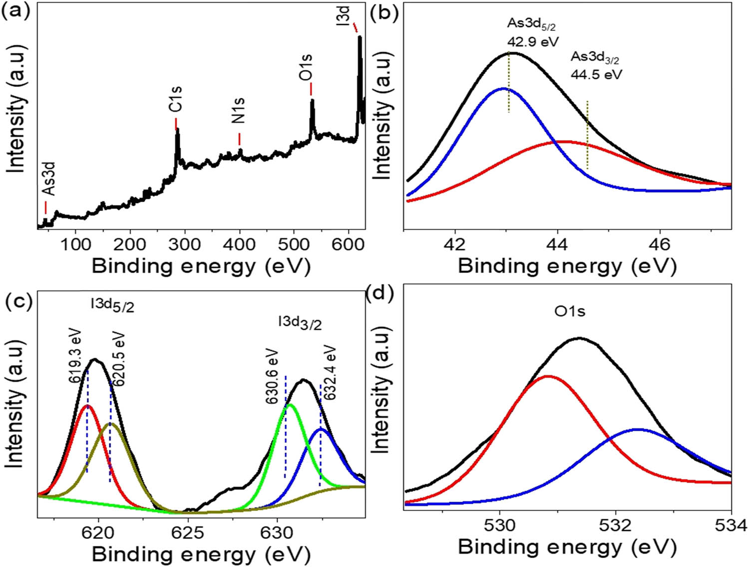
XPS analysis of the As(iii)OI/I-PNMP nanostructured composite, illustrating its chemical composition and elemental states: (a) full survey spectrum confirming the presence of As, O, I, C, and N; (b) high-resolution As 3d spectrum indicating the +3 oxidation state of arsenic; (c) I 3d spectrum showing the coexistence of iodide (I⁻) and oxidized iodine species; and (d) O 1s spectrum.
The survey spectrum displayed in Figure 3(a) confirms the presence of essential elemental components: As, O, I, C, and N. The identification of carbon and nitrogen links back to the organic PNMP matrix, with the C 1s and N 1s peaks located at binding energies around 285.8 and 400.0 eV, respectively. These signals validate the existence of the polymeric backbone, which is vital for structural stabilization and electronic interaction within the composite.
Figure 3(b) provides a detailed analysis of arsenic, demonstrating the high-resolution XPS spectrum of the As 3d orbital, which shows two prominent peaks at 42.9 and 44.5 eV. These peaks correspond to the As 3d5/2 and As 3d3/2 spin–orbit components, respectively, indicating that arsenic is present in the +3 oxidation state (As3+). This finding confirms the presence of trivalent arsenic in the As(iii)OI moiety, aligning with the intended oxidation state in the composite and showcasing successful chemical synthesis and structural preservation. Regarding iodine, the high-resolution spectrum of the I 3d region reveals two distinct doublets. The first doublet appears at 619.3 eV (I 3d5/2) and 630.6 eV (I 3d3/2), associated with iodide ions (I⁻). The second doublet, with peaks at 620.5 and 632.4 eV, pertains to oxidized iodine species, such as molecular iodine (I2) or other higher oxidation states [20]. This mixed oxidation state indicates some redox activity in the composite’s iodine-containing phases. Additionally, the presence of oxygen is confirmed by a prominent O 1s peak at 530.8 eV, which signifies metal–oxygen coordination, especially within the As–O framework. Together, these XPS results support the structural configuration and multi-element integration of the As(iii)OI/I-PNMP NS-composite, highlighting the material’s well-defined and chemically consistent architecture.
Figure 4 illustrates the morphology of the As(iii)OI/I-PNMP composite and the PNMP polymer, utilizing advanced imaging techniques such as SEM, TEM, and 3D surface topography analysis. SEM images (a) and (b) capture the As(iii)OI/I-PNMP composite at various magnifications. The SEM images of the As(iii)OI/I-PNMP composite, captured at different magnifications, reveal a densely packed, hierarchical architecture predominantly consisting of spherical to semi-spherical nanoparticles with an average diameter of approximately 100 nm. These nanoparticles are tightly clustered into larger, cauliflower-like assemblies, a morphology well-known for significantly increasing the accessible surface area. Such an enlarged and texturally rich surface facilitates enhanced catalytic and adsorption performance by offering a greater number of active sites for interaction with arsenic ions. Furthermore, the observed variation in particle size indicates a polydisperse distribution, which can improve packing density and create additional meso- and microporous channels. These structural features collectively contribute to superior arsenic ion adsorption through synergistic effects of high surface area, abundant reactive sites, and improved mass transfer pathways. Also, surface roughness can potentially introduce more interface states, which may act as recombination centers for photogenerated carriers. These interface states can trap electrons or holes, increasing the likelihood of non-radiative recombination and thereby reducing the overall carrier lifetime. However, in certain photocatalytic or photoelectrochemical systems, a moderate increase in roughness can be beneficial, as it enlarges the effective surface area.
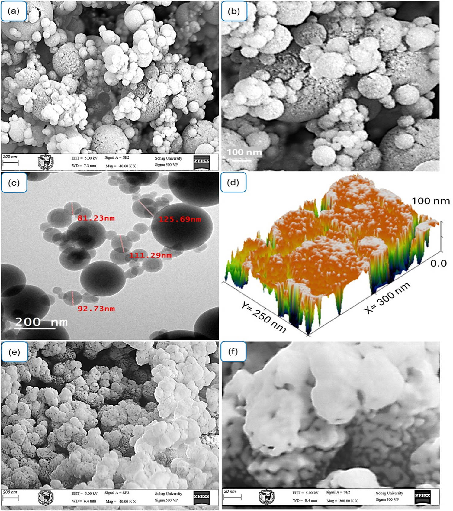
Morphological characterization of As(iii)OI/I-PNMP composite and pure PNMP: (a) and (b) SEM images of the As(iii)OI/I-PNMP composite at different magnifications, (c) TEM image illustrating a uniform spherical morphology of the composite; (d) 3D surface topography and cross-sectional profile of the composite; and (e) and (f) SEM images of pure PNMP at different magnifications.
The TEM analysis in image (c) offers a deeper understanding of the nanoparticles’ size and structural uniformity. The measured particle sizes range from about 81 to 125 nm, which corresponds well with the SEM observations, affirming the nanoscale dimensions of the composite. TEM images also indicate that the particles maintain consistent spherical shapes and are evenly distributed within the matrix, exhibiting minimal aggregation. This uniform dispersion enhances the composite’s performance in applications such as photocatalysis and contaminant adsorption. Moreover, the clear contrast between the cores and edges of the particles might hint at a core-shell structure or variations in composition within.
Image (d) showcases the composite’s 3D surface roughness and cross-sectional structure. The vertical height variation nearly reaches 100 nm, indicating a rough and uneven texture. This surface roughness is crucial for enlarging the overall surface area, significantly boosting the material’s ability to adsorb and interact with pollutants such as As(iii). Additionally, the rough and porous structure may enhance light scattering and absorption characteristics, which is particularly advantageous for photocatalytic and sensor-based applications [21]. In contrast, images (e) and (f) depict the morphology of the pristine PNMP polymer at varying magnifications. Although PNMP also exhibits a spherical form, it appears less densely packed and more porous than the composite. At lower magnification (e), the polymer shows a fluffy, open texture, while higher magnification (f) reveals finer, granulated features on the particle surfaces. This morphology is characteristic of conjugated polymers and is ideal for integrating inorganic components like As(iii) OI. The PNMP matrix offers structural support and stability to the nanoparticles, promoting their uniform distribution.
Thus, the morphological characterization of the As(iii)OI/I-PNMP composite emphasizes its effectiveness as a multifunctional material suitable for environmental and sensing uses. Integrating high surface area, nanoscale characteristics, and structural intricacy from both PNMP and As(iii)OI parts improves its performance and possibilities in practical applications.
3.2 Electrical testing of the As(iii)OI/I-PNMP/PPy optoelectronic device
The electrical characterization of the As(iii)OI/I-PNMP/PPy optoelectronic device was conducted to assess its ability to generate and transport hot electrons when illuminated. This evaluation offers vital insights into the optoelectronic properties of the hybrid nanocomposite system. The device was integrated into a measurement setup utilizing a CHI608E electrochemical workstation, where it underwent linear sweep voltammetry across a wide potential range from –2.0 V to +2.0 V. To guarantee dependable electrical contact, silver paste (Ag paste) was meticulously applied to both ends of the device, serving as effective electrical terminals for connecting to the testing circuit.
The main goal of this electrical assessment was to ascertain the photo-response characteristics of the device, notably the photogenerated current density (J ph), which directly indicates the hot electrons generated from photon absorption. These hot electrons, excited to higher energy states under light exposure, move through the external circuit, producing a measurable photocurrent. The magnitude of this current indicates the optoelectronic performance and photon-harvesting efficiency of the material system.
As depicted in Figure 5(a), the current density versus applied potential (J–V) profiles were captured under both dark (black curve) and illuminated (red curve) conditions. The device exhibited a low and nearly flat current response in darkness, reflecting minimal dark conductivity and negligible leakage current – features that validate excellent off-state behavior. Conversely, under illumination, a notable increase in current density was noted, with the device reaching a peak photocurrent density of about –0.036 mA·cm−2 at –2 V. This marked increase in current under light exposure emphasizes the efficient photon absorption, exciton generation, and charge separation taking place within the active layers.
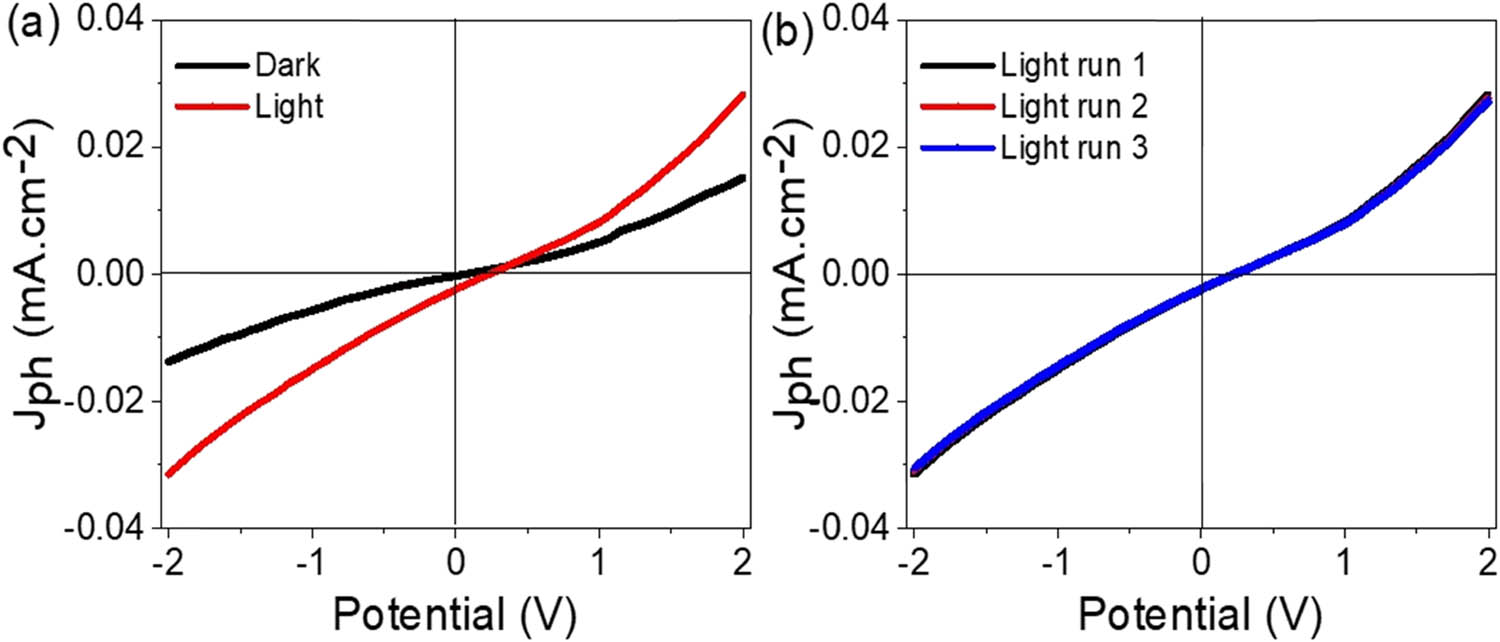
Electrical characterization of the As(iii)OI/I-PNMP/PPy optoelectronic device: (a) linear sweep voltammetry curves recorded under light and dark conditions, highlighting the device’s photoresponse behavior; (b) stability assessment through multiple consecutive illumination cycles, demonstrating reproducibility and operational consistency.
The difference between light-induced and dark current densities determines the J ph. The notably higher J ph when illuminated indicates the synergistic operation of the hybrid components. Integrating As(iii)OI and I-PNMP into the conductive PPy matrix forms a heterojunction that aligns energy levels and enhances effective directional charge transfer. In this process, photoexcited electrons are likely injected into the conduction band of As(iii)OI. At the same time, holes stay in the HOMO of PPy, resulting in efficient electron–hole pair separation and reduced recombination losses.
Figure 5(b) further assesses the device’s photostability through three sequential light exposure cycles, indicated as Light run 1 (black), Light run 2 (red), and Light run 3 (blue). The nearly coinciding J–V curves demonstrate the device’s remarkable reproducibility and stability under continuous illumination. The absence of significant current drift or degradation across the three cycles illustrates the material’s structural durability and its capacity to endure repeated photoexcitation without any loss in performance.
This cyclic durability, in conjunction with robust photo response behavior, indicates that the As(iii)OI/I-PNMP/PPy device is exceptionally well-suited for advanced optoelectronic applications, including photodetectors, UV-Vis light sensors, and opto-switching elements, where long-term operational stability and sensitivity are of paramount importance. In addition, Figure S2 illustrates the stability of the As(iii)OI/I-PNMP/PPy-based device during transitions from dark to light illumination at a small applied potential of 0.1 V, as evaluated through the relationship between time (s) and J ph. The observed stability up to 400 s indicates the device’s capability to operate continuously with excellent stability.
The photoresponse characteristics of the As(iii)OI/I-PNMP/PPy optoelectronic device were systematically examined under different photon energies to understand its sensitivity across a wide spectral range. Figure 6(a) shows the current density–voltage (J–V) characteristics of the device when exposed to various photon energies: 1.7 eV (green), 2.3 eV (blue), 2.8 eV (red), and 3.6 eV (black). These photon energies cover the near-infrared to visible spectrum and approach the UV region, providing a comprehensive overview of the device’s optoelectronic response throughout this energy range.
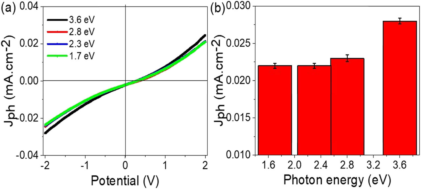
Electrical characterization of the As(iii)OI/I-PNMP/PPy optoelectronic device: (a) Linear sweep voltammetry curves recorded under various photon effects and (b) the estimated J ph values of this optoelectronic device at 2.0 V.
As the energy of the photons increases, a significant enhancement in the photoinduced current density (J ph) is observed. It is noteworthy that at an illumination energy of 3.6 eV, the device demonstrates the highest J ph, attaining a peak of approximately 0.028 mA·cm−2 at a voltage of +2 V. This observed trend strongly suggests that the photogenerated current is directly proportional to the incident photon energy, since photons with higher energy possess a greater capacity to excite charge carriers across the band structure of the material.
The operational principle is closely linked to the electronic bandgap of the As(iii)OI/I-PNMP/PPy hybrid system, estimated at approximately 2.35 eV. When photon energy meets or surpasses this bandgap, efficient photoexcitation takes place, generating electron–hole pairs. Photons with energy equal to or greater than 2.35 eV can elevate electrons from the valence band to the conduction band, thus enhancing charge carrier separation and transport. However, at photon energies below this threshold (e.g., 1.7–2.3 eV), excitation efficiency notably decreases, resulting in lower photocurrent values due to sub-bandgap absorption, which limits electron excitation and diminishes exciton dissociation probability. Figure 6(b) outlines the J ph values obtained under different photon energy exposures, reinforcing the trends observed in Figure 6(a). The bar graph illustrates a steady increase in photocurrent as photon energy rises. The pronounced jump in J ph at 3.2 and 3.6 eV further verifies the optimal spectral responsiveness of the device within and beyond the bandgap range. These findings affirm the device’s effective photoconversion capability, particularly under high-energy light exposure. The As(iii)OI/I-PNMP/PPy optoelectronic device exhibits substantial energy-level alignment and spectral sensitivity, enabling efficient operation under photon energies that approach or exceed its bandgap. The rising J ph correlated with photon energy highlights the system’s promise for high-performance applications, including UV-visible photodetectors, energy-harvesting devices, and multispectral sensors [22].
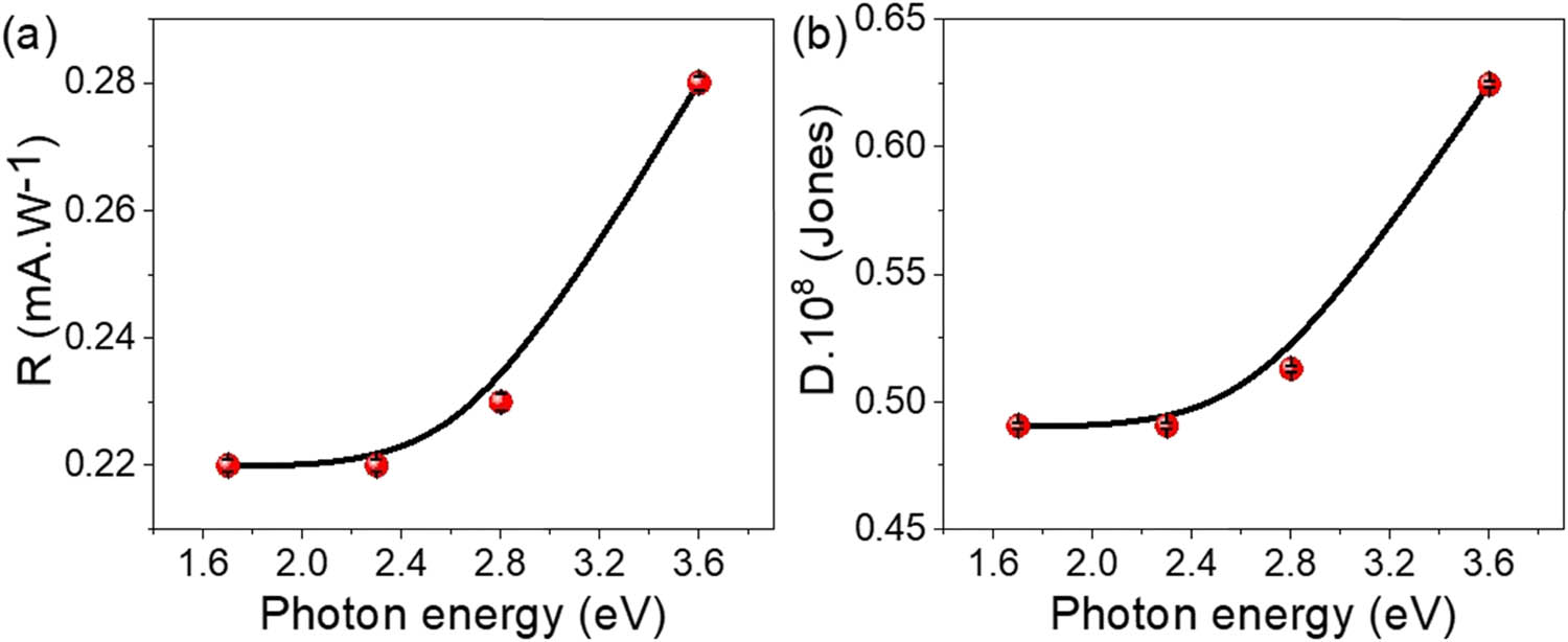
The As(iii)OI/I–PNMP/PPy optoelectronic device’s sensitivity is scientifically characterized by its responsivity (R) and specific detectivity (D), depicted in Figure 7(a) and (b), respectively. These figures provide quantitative insight into the device’s capability to detect and convert incident photons into measurable electrical signals over a range of photon energies. Importantly, the observed photoresponse is in strong agreement with the structural and optical features revealed by our material characterization. XRD and TEM confirm a nanospherical morphology with uniform size distribution, promoting efficient light scattering and enhanced optical path length within the active layer. UV–Vis–NIR analysis indicates a direct bandgap of ∼2.35 eV, which aligns well with the photon energy threshold observed in the R and D trends.
The sensitivity of the fabricated As(iii)OI/I-PNMP/PPy optoelectronic device through the evaluation of the (a) R and (b) D.
As shown in Figure 7(a), R exhibits a non-linear increase with increasing photon energy, with a sharp rise beyond 2.3 eV and a peak of ∼0.28 mA·W⁻¹ at 3.6 eV. This matches the bandgap energy extracted from the optical data, where photons with energies below 2.35 eV (1.6–2.3 eV) are insufficient to excite electrons from the valence band to the conduction band, resulting in minimal carrier generation and low R. Once the photon energy exceeds this structural bandgap, interband electronic transitions are more efficient, yielding a higher density of photogenerated carriers. The nanospherical architecture – confirmed by SEM/TEM – shortens carrier transport paths and increases the effective interfacial area, further aiding separation and collection efficiency.
The specific detectivity (D), shown in Figure 7(b), also rises with photon energy, from ∼0.49 × 10⁸ to 0.63 × 10⁸ Jones. This improvement is attributable to (1) enhanced carrier generation and mobility at energies above the bandgap, as enabled by the composite’s crystalline ordering and conductive polymer network, and (2) a relatively low dark current, which suppresses noise. These structure–property correlations confirm that the superior photodetection performance stems from the interplay between the engineered nanospherical composite morphology, the optimized bandgap, and the efficient charge transport pathways, providing a synchronized relationship between structural characteristics and optical–electronic functionality. These promising values for the device are attributed to the strong correlations between the chemical structure of its constituents, As(iii)OI/I-PNMP/PPy, as determined in Figure S3 (Table 1).
The behavior of the As(iii)OI/I-PNMP/PPy optoelectronic device relative to other devices
| Optoelectronic device | R (mA W−1) | Wavelength (nm) | Potential (V) | D (Jones) |
|---|---|---|---|---|
| MnO2-poly-m-methylaniline [23] | 0.22 | 340 | 2 | 0.47 × 10⁸ |
| TiO2-PANI [24] | 3 × 10⁻³ | 320 | 0 | — |
| Graphene oxide-polypyrrole [25] | 0.1 | 340 | 2 | 0.60 × 10⁸ |
| PC71BM [26] | 0.005 | 300 | 2 | — |
| P3HT [27] | NA | 325 | 1 | — |
| Ppy/CuO [28] | 0.05 | 340 | 1 | 0.8 × 10⁶ |
| CuO/Si Nanowire [29] | 3.8 × 10⁻³ | 405 | 0.2 | — |
| PbI2-5%Ag [30] | NA | 532 | 6 | — |
| ITO/CsPbBr3:ZnO/Ag [31] | 0.01 | 405 | 0 | — |
| Ppy/NiOX [32] | 0.07 | 450 | 2 | 0.5 × 10⁸ |
| ZnO/RGO [33] | 1.3 × 10⁻³ | 350 | 5 | — |
| Graphene/GaN [34] | 3 × 10⁻³ | 365 | 7 | — |
| As(iii)OI/I-PNMP/PPy (this work) | 0.28 | 340 | 2 | 0.63 × 10⁸ |
4 Conclusions
This study reports the successful creation of a novel As(iii)OI/I-PNMP/PPy photodetector through the strategic combination of an n-type As(iii)OI/I-PNMP nanocomposite with a p-type PPy layer, establishing a heterojunction structure. Comprehensive characterization of the synthesized n-type material affirmed its composition and structure. XPS analysis identified arsenic in the As³ oxidation state+, while XRD analysis exhibited a well-defined crystalline structure featuring high-intensity peaks, corresponding to a crystallite size of approximately 21 nm.
The device’s optoelectronic properties were thoroughly examined under various illumination conditions using ultraviolet and visible light. The outcomes indicated a robust photoactive response, as indicated by photogenerated current density (J ph) measurements during light exposure, confirming effective charge generation and transport within the composite material. The photodetector’s R was significantly enhanced, ranging from 0.23 to 0.28 mA/W, illustrating the device’s high sensitivity to incident photons across the visible and ultraviolet spectra. Additionally, the D, a key parameter reflecting the detector’s ability to detect weak optical signals, was found to be between 0.52 × 10⁸ and 0.63 × 10⁸ Jones, emphasizing the exceptional sensing abilities of the developed device. In summary, the integration of As(iii) oxoiodide, iodide-intercalated PNMP, and PPy has facilitated the creation of a highly responsive, broadband photodetector. This hybrid structure represents a promising foundation for future optoelectronic applications, especially in photon sensing, environmental monitoring, and low-intensity light detection technologies.
Acknowledgments
The authors express their gratitude to Princess Nourah bint Abdulrahman University Researchers Supporting Project number (PNURSP2025R223), Princess Nourah bint Abdulrahman University, Riyadh, Saudi Arabia.
-
Funding information: This article is supported by Princess Nourah bint Abdulrahman University Researchers Supporting Project number (PNURSP2025R223), Princess Nourah bint Abdulrahman University, Riyadh, Saudi Arabia.
-
Author contributions: Fatemah H. Alkallas: funding, supervision, and ordering the work; Amira Ben Gouider Trabelsi: writing, revision, and analysis; Asmaa M. Elsayed: supervision and ordering the work; Mohamed Rabia: experimental, analysis, and writing. All authors have accepted responsibility for the entire content of this manuscript and approved its submission.
-
Conflict of interest: The authors state no conflict of interest.
-
Data availability statement: All data generated or analysed during this study are included in this published article.
References
[1] Li G, Xie D, Zhang Q, Zhang M, Liu Z, Wang Z, et al. Interface-engineered non-volatile visible-blind photodetector for in-sensor computing. Nat Commun. 2024;16(1):1–10. (2025). 10.1038/s41467-024-55412-6.Suche in Google Scholar PubMed PubMed Central
[2] Alkallas FH, Rabia M, Kusmartsev FV, Trabelsi ABG. A thin film optoelectronic photodetector of spherical and linear resonators via one-pot synthesis of Bi(iii) oxide/polypyrrole nanocomposite. Sci Rep. 2025;15(1):1–11. 10.1038/s41598-025-86092-x.Suche in Google Scholar PubMed PubMed Central
[3] Wu D, Guo C, Zeng L, Ren X, Shi Z, Wen L, et al. Phase-controlled van der Waals growth of wafer-scale 2D MoTe2 layers for integrated high-sensitivity broadband infrared photodetection. Light: Sci Appl. 2023;12(1):1–12. 10.1038/s41377-022-01047-5.Suche in Google Scholar PubMed PubMed Central
[4] Salih EY. Opto-electrical evaluation of visible blind fast-response nanostructured SnO2/Si photodetector. RSC Adv. 2024;14:27733–40. 10.1039/D4RA05303F.Suche in Google Scholar PubMed PubMed Central
[5] Sulaman M, Yang S, Imran A, Zhang Z, Bukhtiar A, Ge Z, et al. Two bulk-heterojunctions made of blended hybrid nanocomposites for high-performance broadband, self-driven photodetectors. ACS Appl Mater Interfaces. 2023;15(21):25671–83. 10.1021/acsami.3c01749.Suche in Google Scholar PubMed
[6] Yahya Salih E, Ramizy A, Sabbar Mohammed A, Hassan Ibnaouf K, Hassan Eisa M, Aldaghri O. Photo-responsive analysis of branchy dendrites-like CuO/PS p-n junction visible light photodetector. Mater Sci Eng: B. 2024;301:117172. 10.1016/J.MSEB.2023.117172.Suche in Google Scholar
[7] Patel RP, Pataniya PM, Patel M, Adepu V, Sahatiya P, Sumesh CK. Highly flexible and foldable broad band WSe2/CuO heterostructure photodetector. Sens Actuators A: Phys. 2023;356:114339. 10.1016/J.SNA.2023.114339.Suche in Google Scholar
[8] Algadi H, Mahata C, Kim S, Dalapati GK. Improvement of photoresponse properties of self-powered ITO/InP Schottky junction photodetector by interfacial ZnO passivation. J Electron Mater. 2020;50(4):1800–6. 10.1007/S11664-020-08565-1.Suche in Google Scholar
[9] He Z, Zhang S, Zheng L, Liu Z, Zhang G, Wu H, et al. Si-based NIR tunneling heterojunction photodetector with interfacial engineering and 3D-graphene integration. IEEE Electron Device Lett. 2022;43:1818–21. 10.1109/LED.2022.3203474.Suche in Google Scholar
[10] Wu H, Liu Z, Wang B, Zheng L, Lian S, Zhang J, et al. Integration of PbS quantum dots with 3D-graphene for self-powered broadband photodetectors in image sensors. ACS Photonics. 2024;11:1342–51. 10.1021/ACSPHOTONICS.3C01803/SUPPL_FILE/PH3C01803_SI_001.PDF.Suche in Google Scholar
[11] Dědek I, Kupka V, Jakubec P, Šedajová V, Jayaramulu K, Otyepka M. Metal-organic framework/conductive polymer hybrid materials for supercapacitors. Appl Mater Today. 2022;26:101387. 10.1016/J.APMT.2022.101387.Suche in Google Scholar
[12] Matysiak W, Tański T, Smok W, Gołombek K, Schab-Balcerzak E. Effect of conductive polymers on the optical properties of electrospun polyacrylonitryle nanofibers filled by polypyrrole, polythiophene and polyaniline. Appl Surf Sci. 2020;509:145068. 10.1016/J.APSUSC.2019.145068.Suche in Google Scholar
[13] Alkallas FH, Mahmoud A, Abd M, Ben A, Trabelsi G. Eminent Red Sea water hydrogen generation via a Pb (II) -iodide/poly (1 H -pyrrole) nanocomposite photocathode; 2024.10.1515/gps-2024-0048Suche in Google Scholar
[14] Alnuwaiser MA, Rabia M. A highly promising flower-shaped WO2I2/Poly(1H-Pyrrole) nanocomposite thin film as a potentiometric sensor for the detection of Cd2+ ions in water. J Compos Sci. 2023;7:439. 10.3390/JCS7100439.Suche in Google Scholar
[15] Trabelsi ABG, Alkallas FH, Kusmartsev FV, Rabia M. Bi2O3–BiOCl/poly-m-methyl aniline nanocomposite thin film for broad-spectrum light-sensing. Green Process Synth. 2024;13(1):20240160. 10.1515/gps-2024-0160.Suche in Google Scholar
[16] Burton AW, Ong K, Rea T, Chan IY. On the estimation of average crystallite size of zeolites from the Scherrer equation: A critical evaluation of its application to zeolites with one-dimensional pore systems. Microporous Mesoporous Mater. 2009;117:75–90. 10.1016/J.MICROMESO.2008.06.010.Suche in Google Scholar
[17] Lim DJ, Marks NA, Rowles MR. Universal Scherrer equation for graphene fragments. Carbon. 2020;162:475–80. 10.1016/J.CARBON.2020.02.064.Suche in Google Scholar
[18] Haryński Ł, Olejnik A, Grochowska K, Siuzdak K. A facile method for Tauc exponent and corresponding electronic transitions determination in semiconductors directly from UV–Vis spectroscopy data. Opt Mater. 2022;127:112205. 10.1016/J.OPTMAT.2022.112205.Suche in Google Scholar
[19] Baishya K, Ray JS, Dutta P, Das PP, Das SK. Graphene-mediated band gap engineering of WO3 nanoparticle and a relook at Tauc equation for band gap evaluation. Appl Phys A: Mater Sci Process. 2018;124:1–6. 10.1007/S00339-018-2097-0/FIGURES/5.Suche in Google Scholar
[20] Rabia M, Elsayed AM, Alnuwaiser MA. Highly morphological behavior AgI/P1HP intercalated with iodide ions in the polymer chains as a promising photocathode for the hydrogen generation from Red Sea water. Opt Quantum Electron. 2024;56:1–16. 10.1007/S11082-023-06274-7/METRICS.Suche in Google Scholar
[21] Omotosho K, Tran J, Shevchenko EV, Berman D. Polymer infiltration synthesis of inorganic nanoporous coatings: Does polymer template affect their properties? Surf Coat Technol. 2023;452:129107. 10.1016/J.SURFCOAT.2022.129107.Suche in Google Scholar
[22] Che Y, Zhang H, Abdiryim T, Jamal R, Kadir A, Helil Z, et al. Ultraviolet photodetectors based on TiO2 nanorod arrays/PEDOT-type conducting polymers. Opt Mater. 2021;122:111805. 10.1016/J.OPTMAT.2021.111805.Suche in Google Scholar
[23] Aldosari E, Rabia M, Ewais HA, Song K. One-pot synthesis of a network of Mn2O3-MnO2-poly(m-methylaniline) composite nanorods on a polypyrrole film presents a promising and efficient optoelectronic and solar cell device. Open Chem. 2024;22(1):20240039. 10.1515/chem-2024-0039.Suche in Google Scholar
[24] Zheng L, Yu P, Hu K, Teng F, Chen H, Fang X. Scalable-production, self-powered TiO2 nanowell-organic hybrid UV photodetectors with tunable performances. ACS Appl Mater Interfaces. 2016;8:33924–32. 10.1021/acsami.6b11012.Suche in Google Scholar PubMed
[25] Trabelsi ABG, Elsayed AM, Alkallas FH, AlFaify S, Shkir M, Alrebdi TA, et al. Photodetector-based material from a highly sensitive free-standing graphene oxide/polypyrrole nanocomposite. Coatings. 2023;13:1198. 10.3390/COATINGS13071198.Suche in Google Scholar
[26] Qi J, Han J, Zhou X, Yang D, Zhang J, Qiao W, et al. Optimization of broad-response and high-detectivity polymer photodetectors by bandgap engineering of weak donor-strong acceptor polymers. Macromolecules. 2015;48:3941–8. 10.1021/ACS.MACROMOL.5B00859/SUPPL_FILE/MA5B00859_SI_001.PDF.Suche in Google Scholar
[27] Tan WC, Shih WH, Chen YF. A highly sensitive graphene-organic hybrid photodetector with a piezoelectric substrate. Adv Funct Mater. 2014;24:6818–25. 10.1002/ADFM.201401421.Suche in Google Scholar
[28] Sendi RK, Al-Harbi N, Atta A, Rabia M, Abdelhamied MM. Copper oxide and copper nanoparticles insertion within a PPy matrix for photodetector applications. Opt Quantum Electron. 2023;55:1–15. 10.1007/S11082-023-05226-5/METRICS.Suche in Google Scholar
[29] Hong Q, Cao Y, Xu J, Lu H, He J, Sun JL. Self-powered ultrafast broadband photodetector based on p-n heterojunctions of CuO/Si nanowire array. ACS Appl Mater Interfaces. 2014;6:20887–94. 10.1021/AM5054338.Suche in Google Scholar PubMed
[30] Ismail RA, Mousa AM, Shaker SS. Visible-enhanced silver-doped PbI2 nanostructure/Si heterojunction photodetector: effect of doping concentration on photodetector parameters. Opt Quantum Electron. 2019;51:1–19. 10.1007/S11082-019-2063-X/TABLES/4.Suche in Google Scholar
[31] Perveen A, Movsesyan A, Abubakar SM, Saeed F, Hussain S, Raza A, et al. In-situ fabricated and plasmonic enhanced MACsPbBr3-polymer composite perovskite film based UV photodetector. J Mol Structure. 2023;1279:134962. 10.1016/J.MOLSTRUC.2023.134962.Suche in Google Scholar
[32] Atta A, Abdeltwab E, Negm H, Al-Harbi N, Rabia M, Abdelhamied MM. Characterization and linear/non-linear optical properties of polypyrrole/NiO for optoelectronic devices. Inorg Chem Commun. 2023;152:110726. 10.1016/J.INOCHE.2023.110726.Suche in Google Scholar
[33] Liu K, Sakurai M, Liao M, Aono M. Giant improvement of the performance of ZnO nanowire photodetectors by Au nanoparticles. J Phys Chem C. 2010;114:19835–39. 10.1021/jp108320j.Suche in Google Scholar
[34] Kalra A, Vura S, Rathkanthiwar S, Muralidharan R, Raghavan S, Nath DN. Demonstration of high-responsivity epitaxial β-Ga2O3/GaN metal-heterojunction-metal broadband UV-A/UV-C detector. Appl Phys Express. 2018;11:064101. 10.7567/APEX.11.064101.Suche in Google Scholar
© 2025 the author(s), published by De Gruyter
This work is licensed under the Creative Commons Attribution 4.0 International License.
Artikel in diesem Heft
- Research Articles
- Single-step fabrication of Ag2S/poly-2-mercaptoaniline nanoribbon photocathodes for green hydrogen generation from artificial and natural red-sea water
- Abundant new interaction solutions and nonlinear dynamics for the (3+1)-dimensional Hirota–Satsuma–Ito-like equation
- A novel gold and SiO2 material based planar 5-element high HPBW end-fire antenna array for 300 GHz applications
- Explicit exact solutions and bifurcation analysis for the mZK equation with truncated M-fractional derivatives utilizing two reliable methods
- Optical and laser damage resistance: Role of periodic cylindrical surfaces
- Numerical study of flow and heat transfer in the air-side metal foam partially filled channels of panel-type radiator under forced convection
- Water-based hybrid nanofluid flow containing CNT nanoparticles over an extending surface with velocity slips, thermal convective, and zero-mass flux conditions
- Dynamical wave structures for some diffusion--reaction equations with quadratic and quartic nonlinearities
- Solving an isotropic grey matter tumour model via a heat transfer equation
- Study on the penetration protection of a fiber-reinforced composite structure with CNTs/GFP clip STF/3DKevlar
- Influence of Hall current and acoustic pressure on nanostructured DPL thermoelastic plates under ramp heating in a double-temperature model
- Applications of the Belousov–Zhabotinsky reaction–diffusion system: Analytical and numerical approaches
- AC electroosmotic flow of Maxwell fluid in a pH-regulated parallel-plate silica nanochannel
- Interpreting optical effects with relativistic transformations adopting one-way synchronization to conserve simultaneity and space–time continuity
- Modeling and analysis of quantum communication channel in airborne platforms with boundary layer effects
- Theoretical and numerical investigation of a memristor system with a piecewise memductance under fractal–fractional derivatives
- Tuning the structure and electro-optical properties of α-Cr2O3 films by heat treatment/La doping for optoelectronic applications
- High-speed multi-spectral explosion temperature measurement using golden-section accelerated Pearson correlation algorithm
- Dynamic behavior and modulation instability of the generalized coupled fractional nonlinear Helmholtz equation with cubic–quintic term
- Study on the duration of laser-induced air plasma flash near thin film surface
- Exploring the dynamics of fractional-order nonlinear dispersive wave system through homotopy technique
- The mechanism of carbon monoxide fluorescence inside a femtosecond laser-induced plasma
- Numerical solution of a nonconstant coefficient advection diffusion equation in an irregular domain and analyses of numerical dispersion and dissipation
- Numerical examination of the chemically reactive MHD flow of hybrid nanofluids over a two-dimensional stretching surface with the Cattaneo–Christov model and slip conditions
- Impacts of sinusoidal heat flux and embraced heated rectangular cavity on natural convection within a square enclosure partially filled with porous medium and Casson-hybrid nanofluid
- Stability analysis of unsteady ternary nanofluid flow past a stretching/shrinking wedge
- Solitonic wave solutions of a Hamiltonian nonlinear atom chain model through the Hirota bilinear transformation method
- Bilinear form and soltion solutions for (3+1)-dimensional negative-order KdV-CBS equation
- Solitary chirp pulses and soliton control for variable coefficients cubic–quintic nonlinear Schrödinger equation in nonuniform management system
- Influence of decaying heat source and temperature-dependent thermal conductivity on photo-hydro-elasto semiconductor media
- Dissipative disorder optimization in the radiative thin film flow of partially ionized non-Newtonian hybrid nanofluid with second-order slip condition
- Bifurcation, chaotic behavior, and traveling wave solutions for the fractional (4+1)-dimensional Davey–Stewartson–Kadomtsev–Petviashvili model
- New investigation on soliton solutions of two nonlinear PDEs in mathematical physics with a dynamical property: Bifurcation analysis
- Mathematical analysis of nanoparticle type and volume fraction on heat transfer efficiency of nanofluids
- Creation of single-wing Lorenz-like attractors via a ten-ninths-degree term
- Optical soliton solutions, bifurcation analysis, chaotic behaviors of nonlinear Schrödinger equation and modulation instability in optical fiber
- Chaotic dynamics and some solutions for the (n + 1)-dimensional modified Zakharov–Kuznetsov equation in plasma physics
- Fractal formation and chaotic soliton phenomena in nonlinear conformable Heisenberg ferromagnetic spin chain equation
- Single-step fabrication of Mn(iv) oxide-Mn(ii) sulfide/poly-2-mercaptoaniline porous network nanocomposite for pseudo-supercapacitors and charge storage
- Novel constructed dynamical analytical solutions and conserved quantities of the new (2+1)-dimensional KdV model describing acoustic wave propagation
- Tavis–Cummings model in the presence of a deformed field and time-dependent coupling
- Spinning dynamics of stress-dependent viscosity of generalized Cross-nonlinear materials affected by gravitationally swirling disk
- Design and prediction of high optical density photovoltaic polymers using machine learning-DFT studies
- Robust control and preservation of quantum steering, nonlocality, and coherence in open atomic systems
- Coating thickness and process efficiency of reverse roll coating using a magnetized hybrid nanomaterial flow
- Dynamic analysis, circuit realization, and its synchronization of a new chaotic hyperjerk system
- Decoherence of steerability and coherence dynamics induced by nonlinear qubit–cavity interactions
- Finite element analysis of turbulent thermal enhancement in grooved channels with flat- and plus-shaped fins
- Modulational instability and associated ion-acoustic modulated envelope solitons in a quantum plasma having ion beams
- Statistical inference of constant-stress partially accelerated life tests under type II generalized hybrid censored data from Burr III distribution
- On solutions of the Dirac equation for 1D hydrogenic atoms or ions
- Entropy optimization for chemically reactive magnetized unsteady thin film hybrid nanofluid flow on inclined surface subject to nonlinear mixed convection and variable temperature
- Stability analysis, circuit simulation, and color image encryption of a novel four-dimensional hyperchaotic model with hidden and self-excited attractors
- A high-accuracy exponential time integration scheme for the Darcy–Forchheimer Williamson fluid flow with temperature-dependent conductivity
- Novel analysis of fractional regularized long-wave equation in plasma dynamics
- Development of a photoelectrode based on a bismuth(iii) oxyiodide/intercalated iodide-poly(1H-pyrrole) rough spherical nanocomposite for green hydrogen generation
- Investigation of solar radiation effects on the energy performance of the (Al2O3–CuO–Cu)/H2O ternary nanofluidic system through a convectively heated cylinder
- Quantum resources for a system of two atoms interacting with a deformed field in the presence of intensity-dependent coupling
- Studying bifurcations and chaotic dynamics in the generalized hyperelastic-rod wave equation through Hamiltonian mechanics
- A new numerical technique for the solution of time-fractional nonlinear Klein–Gordon equation involving Atangana–Baleanu derivative using cubic B-spline functions
- Interaction solutions of high-order breathers and lumps for a (3+1)-dimensional conformable fractional potential-YTSF-like model
- Hydraulic fracturing radioactive source tracing technology based on hydraulic fracturing tracing mechanics model
- Numerical solution and stability analysis of non-Newtonian hybrid nanofluid flow subject to exponential heat source/sink over a Riga sheet
- Numerical investigation of mixed convection and viscous dissipation in couple stress nanofluid flow: A merged Adomian decomposition method and Mohand transform
- Effectual quintic B-spline functions for solving the time fractional coupled Boussinesq–Burgers equation arising in shallow water waves
- Analysis of MHD hybrid nanofluid flow over cone and wedge with exponential and thermal heat source and activation energy
- Solitons and travelling waves structure for M-fractional Kairat-II equation using three explicit methods
- Impact of nanoparticle shapes on the heat transfer properties of Cu and CuO nanofluids flowing over a stretching surface with slip effects: A computational study
- Computational simulation of heat transfer and nanofluid flow for two-sided lid-driven square cavity under the influence of magnetic field
- Irreversibility analysis of a bioconvective two-phase nanofluid in a Maxwell (non-Newtonian) flow induced by a rotating disk with thermal radiation
- Hydrodynamic and sensitivity analysis of a polymeric calendering process for non-Newtonian fluids with temperature-dependent viscosity
- Exploring the peakon solitons molecules and solitary wave structure to the nonlinear damped Kortewege–de Vries equation through efficient technique
- Modeling and heat transfer analysis of magnetized hybrid micropolar blood-based nanofluid flow in Darcy–Forchheimer porous stenosis narrow arteries
- Activation energy and cross-diffusion effects on 3D rotating nanofluid flow in a Darcy–Forchheimer porous medium with radiation and convective heating
- Insights into chemical reactions occurring in generalized nanomaterials due to spinning surface with melting constraints
- Influence of a magnetic field on double-porosity photo-thermoelastic materials under Lord–Shulman theory
- Soliton-like solutions for a nonlinear doubly dispersive equation in an elastic Murnaghan's rod via Hirota's bilinear method
- Analytical and numerical investigation of exact wave patterns and chaotic dynamics in the extended improved Boussinesq equation
- Nonclassical correlation dynamics of Heisenberg XYZ states with (x, y)-spin--orbit interaction, x-magnetic field, and intrinsic decoherence effects
- Exact traveling wave and soliton solutions for chemotaxis model and (3+1)-dimensional Boiti–Leon–Manna–Pempinelli equation
- Unveiling the transformative role of samarium in ZnO: Exploring structural and optical modifications for advanced functional applications
- On the derivation of solitary wave solutions for the time-fractional Rosenau equation through two analytical techniques
- Analyzing the role of length and radius of MWCNTs in a nanofluid flow influenced by variable thermal conductivity and viscosity considering Marangoni convection
- Advanced mathematical analysis of heat and mass transfer in oscillatory micropolar bio-nanofluid flows via peristaltic waves and electroosmotic effects
- Exact bound state solutions of the radial Schrödinger equation for the Coulomb potential by conformable Nikiforov–Uvarov approach
- Some anisotropic and perfect fluid plane symmetric solutions of Einstein's field equations using killing symmetries
- Nonlinear dynamics of the dissipative ion-acoustic solitary waves in anisotropic rotating magnetoplasmas
- Curves in multiplicative equiaffine plane
- Exact solution of the three-dimensional (3D) Z2 lattice gauge theory
- Propagation properties of Airyprime pulses in relaxing nonlinear media
- Symbolic computation: Analytical solutions and dynamics of a shallow water wave equation in coastal engineering
- Wave propagation in nonlocal piezo-photo-hygrothermoelastic semiconductors subjected to heat and moisture flux
- Comparative reaction dynamics in rotating nanofluid systems: Quartic and cubic kinetics under MHD influence
- Laplace transform technique and probabilistic analysis-based hypothesis testing in medical and engineering applications
- Physical properties of ternary chloro-perovskites KTCl3 (T = Ge, Al) for optoelectronic applications
- Gravitational length stretching: Curvature-induced modulation of quantum probability densities
- The search for the cosmological cold dark matter axion – A new refined narrow mass window and detection scheme
- A comparative study of quantum resources in bipartite Lipkin–Meshkov–Glick model under DM interaction and Zeeman splitting
- PbO-doped K2O–BaO–Al2O3–B2O3–TeO2-glasses: Mechanical and shielding efficacy
- Nanospherical arsenic(iii) oxoiodide/iodide-intercalated poly(N-methylpyrrole) composite synthesis for broad-spectrum optical detection
- Sine power Burr X distribution with estimation and applications in physics and other fields
- Numerical modeling of enhanced reactive oxygen plasma in pulsed laser deposition of metal oxide thin films
- Dynamical analyses and dispersive soliton solutions to the nonlinear fractional model in stratified fluids
- Computation of exact analytical soliton solutions and their dynamics in advanced optical system
- An innovative approximation concerning the diffusion and electrical conductivity tensor at critical altitudes within the F-region of ionospheric plasma at low latitudes
- An analytical investigation to the (3+1)-dimensional Yu–Toda–Sassa–Fukuyama equation with dynamical analysis: Bifurcation
- Swirling-annular-flow-induced instability of a micro shell considering Knudsen number and viscosity effects
- Review Article
- Examination of the gamma radiation shielding properties of different clay and sand materials in the Adrar region
- Erratum
- Erratum to “On Soliton structures in optical fiber communications with Kundu–Mukherjee–Naskar model (Open Physics 2021;19:679–682)”
- Special Issue on Fundamental Physics from Atoms to Cosmos - Part II
- Possible explanation for the neutron lifetime puzzle
- Special Issue on Nanomaterial utilization and structural optimization - Part III
- Numerical investigation on fluid-thermal-electric performance of a thermoelectric-integrated helically coiled tube heat exchanger for coal mine air cooling
- Special Issue on Nonlinear Dynamics and Chaos in Physical Systems
- Analysis of the fractional relativistic isothermal gas sphere with application to neutron stars
- Abundant wave symmetries in the (3+1)-dimensional Chafee–Infante equation through the Hirota bilinear transformation technique
- Successive midpoint method for fractional differential equations with nonlocal kernels: Error analysis, stability, and applications
- Novel exact solitons to the fractional modified mixed-Korteweg--de Vries model with a stability analysis