
Research on AFM tip-related nanofabrication of two-dimensional materials
-
Meng Li


Abstract
With the great success of graphene, two-dimensional (2D) materials, thanks to their fascinating electronic and optoelectronic properties, have aroused extensive attention among the scientific community. Broad research efforts have proven the enormous potential of 2D materials in optoelectronics, electrochemistry, spintronics, energy storage, catalysis, biomedicine, and many other fields. Driven by the promising applications of 2D materials, there has been an emerging trend toward nanofabricating 2D materials with customized parameters, which are essential for tailor-making controllable artificial nanostructures used in building sophisticated 2D material systems. As the most commonly used solid probe lithography technique, atomic force microscopy (AFM) integrates visualization and multi-mode fabrication within one system, demonstrating its superior capability in the nanofabrication of 2D materials. In view of this, in this review article, we offer a brief introduction to how AFM nanofabrication works and the classification of AFM nanofabrication techniques by the tip-sample surface interaction. Following that, we discuss the results of 2D material nanofabrication by mechanical, thermal, electrical, and other AFM techniques in which external stimulations are applied on special AFM probes.
1 Introduction
1.1 Unique properties and emerging applications of 2D materials
Although layered materials have existed and been studied for more than a century, their true potential was not revealed until the first piece of graphene flake was mechanically peeled from an insulating substrate. Since then, two dimensional (2D) materials with very unique properties have become one of the most extensively studied types of materials. As a popular member of the 2D family, graphene has emerged as a hot subject of research due to its remarkable properties. These include an electric conductivity of 15,000 cm2 V−1 s−1 at room temperature and up to 200,000 cm2 V−1 s−1 for defect-free suspended graphene in theory, a Young’s modulus of approximately 1 TPa, a thermal conductivity of 3,000–5,000 W m−1 K−1, and a light absorption of 2.3% with a negligible reflectance of <0.1%. It also features exceptional flexibility and transparency, lightweight, and matchless thinness and chemical stability [1]. These outstanding properties have made graphene an important material for use in a broad range of applications, such as electronics, optoelectronics, high-strength materials, catalysts, chemical sensors and biosensors, and energy storage and conversion devices [2,3].
Besides uncovering the enormous potential of graphene itself, the burgeoning research on graphene has also evoked a surge of scientific enthusiasm toward the other members of the 2D family, especially when the gapless nature of graphene proves to be a hindrance to tapping into its full potential. Following the discovery of graphene, a wide spectrum of novel layered materials, which were originally deemed to merely exist in the realm of theory, have been synthesized and extensively investigated. These materials can be divided into two main categories: compounds and allotropes [4]. As a part of the former group, transition metal dichalcogenides (TMDs) are a class of 2D materials with a chemical formula expressed as MX2. Specifically, X stands for a chalcogen atom and M for a transition metal atom sandwiched between two X atoms. As a promising alternative, TMDs undergo an indirect to direct band gap crossover from approximately 1.2–1.9 eV as their thickness decreases from bulk to monolayer, which can make up the limitation of graphene. Besides a tunable band gap, TMDs feature both abundant atomic combinations and rich phases such as 1T (trigonal symmetry), 2R (hexagonal symmetry), and 3R (rhombohedral symmetry), offering diverse choices of topological insulators, semiconductors, metals, semimetals, and superconductors [5]. With a unique electronic structure, TMDs have a series of distinct properties that distinguish it from their bulk counterparts, such as a high current on-off ratio [6], moderate mobility [7], an outstanding photo-switching ability [8], a large specific surface area, and strong spin–orbit coupling [9]. These unique properties make TMDs suitable for use in the fabrication of modern electronics, optoelectronics, flexible devices, spintronics, among others [10,11,12,13].
As the only insulating material in the 2D family to date, hexagonal boron nitride (h-BN) consists of boron (B) and nitrogen (N) atoms arranged in a sp2 hybridized honeycomb-shaped lattice network. h-BN has a graphene-like structure that offers comparably high thermal conductivity to graphene. In addition, it features multiple favorable properties, such as a large band gap (5.822–5.968 eV), exotic opto-electrical properties, high mechanical robustness, temperature sustainability, excellent chemical inertness, and attractive piezoelectric responses. These advantages demonstrate its huge potential as an ideal substrate for application in gate dielectric materials, tunneling barriers, gate dielectric barriers, deep ultraviolet light sources, photodetectors, single-photon emitters, and sensors [14,15,16,17,18].
For the latter group, silicene, germanane, and phosphorene, for example, have been studied much less compared to graphene, TMDs, and h-BN. Although several theoretical studies have shown their unique flexibility, compressibility, and many other properties superior to those of the other 2D materials [19,20], only a few experimental applications of mono-elemental 2D materials have been reported to date. The key reason is the thermodynamical instability and tendency toward oxidation, which will lead to a complicated preparation process, limited availability, and fast degradation of these mono-elemental sheets. Despite this fact, the research on mono-elemental 2D materials is still growing rapidly, a typical application of which is Mxene. It is believed that they will emerge as strong contenders in the realm of 2D materials if their true potential can be unlocked in the near future [21].
1.2 Nanofabrication of 2D materials and the prominent role of atomic force microscope (AFM)
As covered earlier, due to the intriguing functionalities endowed by their 2D nature, 2D materials have been widely investigated to explore their application in next-generation electronics and optoelectronics. This has opened up new opportunities to fabricate devices and even integrated systems based on 2D materials, such as nanoplate arrays, smart electric circuits, and lab-on-a-chip systems. From the technological point of view, the nanofabrication of 2D materials with customized parameters, such as controllable thickness, a regular shape, or a specific size, is the prerequisite for building sophisticated 2D materials-based systems [22]. Nanofabrication techniques can be used to significantly improve the integration and performance of 2D materials-based devices. Moreover, the ability of nanofabrication techniques to adjust the size and shape of a structure at nanometer scale (or nanoscale) makes it possible to customize and control the intrinsic mechanical, chemical, electrical, optical, and other properties of 2D materials to fit different applications [23]. For instance, nanofabrication techniques can modify the carrier type and concentration [24] or perform semiconducting-to-metallic transition [25] and thereby create vacancies, dopants, functional groups, grain boundaries, or edges in 2D materials to customize electrical properties. These techniques can also be used to introduce interesting optical properties, such as drastically altered photoluminescence (PL) spectra and long-lived excitonic transition [26]. They can also tailor physicochemical properties by adjusting the level of electrocatalytic activity [27]. These applications demonstrate that it is necessary to go beyond the 2D materials themselves by nanofabricating them to build sophisticated and high-performance 2D materials-based devices and systems. Proper nanofabrication techniques are the key to achieving that end.
Nanofabrication refers to the ability to construct sub-100 nm structures to build components or devices with desired properties and performance or to integrate nanoscale components into complicated systems [28]. Nanofabrication techniques can be categorized into three main types: planar techniques, mold techniques, and probe techniques [29,30,31]. The characteristics of 2D materials, such as the large lateral surface, ultra-small thickness, and high sensitivity to external factors, pose challenges to the nanofabrication of them using conventional planar and mold techniques. These include the limited size or resolution, the extremely high cost of masks with nanoscale precision, and the limited flexibility. Unlike these conventional techniques, probe techniques, either equipped with non-solid probes with focused beams of laser, photons/electrons, ions, and atoms, or solid sharp probes, do not require a mask to achieve nanoscale or even atomic-resolution fabrication. They have emerged as a flexible and high precision alternative for nanofabrication of 2D materials. Non-solid probe-based nanofabrication techniques come with focused beams of electrons or ions to form an irradiation probe. Examples include electron beam lithography (EBL) and flare-based lithography. Through the interaction between the energetic electrons/ions and the surface of the solid material, non-solid probe techniques can be used to construct nanostructures or nanopatterns with nanoscale or even sub-nanometer precision. With this powerful capability, these techniques are now widely used in the nanofabrication of 2D materials [32,33]. Despite the considerable progress, major problems still remain when it comes to processing the atomically thin 2D layers. For instance, when the electron/ion beam bombards on the surface of the target sample, a variety of physical and chemical phenomena will occur to cause a collection of nanoscale effects. This may in turn bring unpredictable electron/ion implantation damage, vacancy, and dislocation, thus causing the 2D materials to deteriorate. Meanwhile, non-solid probes are commonly fabricated by resistive materials, which may increase the risk of contamination and cause some damage as 2D materials are known to be sensitive to resistive residues [34].
Unlike non-solid probe nanofabrication, solid probe nanofabrication techniques typically adopt a solid, sharp metal probe and work based on scanning probe microscopy. Furthermore, the solid probe nanofabrication technique is highly appealing due to its ability to achieve sub-10 nm resolution in a single step process [35]. By controlling the position of the probe and the underneath sample surface within the contact or near contact nanoscale region, solid probe nanofabrication can be performed in a single step without using any mask or resistive material. In general, the scanning tunnelling microscope (STM) and AFM are the most popular microscopies in the scanning probe microscopy family, which can be implemented with the principles of quantum tunnelling effect and contact force control between the tip and sample, respectively. In contrast to STM that suffers from the limitations of conductive samples, vacuum operating conditions and inability to monitor force variations [36,37], AFM operates by measuring the attractive or repulsive force generated by the van der Waals interaction between the probe and sample. This suggests that AFM is applicable for a wider range of materials, such as insulators, semiconductors, and conductors, and working environments, such as ambient liquid conditions, varying temperatures or moistures, and vacuum conditions, than STM [38]. Moreover, AFM has multiple operation modes that allow researchers to capture information on surface properties in terms of physics, chemistry, biology, biochemistry, engineering, technology, and other disciplines from atomic to molecular resolution. Besides providing useful information [39], AFM can integrate visualization and fabrication within one system and its cantilevered tip can be loaded with a variety of sources, including mechanical, thermal, electrical, chemical, and phonic ones, to initiate and perform different fabrication processes. Although the industrial use of AFM is greatly hindered by the inadequate device performance, inconsistent outcomes, and limited throughputs, extensive efforts have been made to improve its reproducibility and productivity in nanofabrication. These include implementing automation, developing hardware or software, and integrating parallel arrays of probes and probe speed increasing devices into AFM systems. These efforts point to a promising future of AFM nanofabrication in large-area and high-speed patterning. The abovementioned capabilities and enhancements make AFM an appealing approach for the nanofabrication of 2D materials [40,41].
Hence, in this review article, we focus specifically on recent advances in the AFM nanofabrication of 2D materials. First, we briefly introduce the working principle of AFM nanofabrication and related techniques. Then, from the perspective of the working principle, we discuss four types of AFM tip-related nanofabrication techniques: mechanical, thermal and thermochemical, electrical and electrochemical, and other AFM nanofabrication techniques. The representative experimental examples of AFM tip-related fabrication on 2D materials from recent literature are shown in each section.
2 Working principle of AFM nanofabrication
2.1 AFM setup and their mechanisms
As shown in Figure 1(a), a typical AFM mainly consists of a cantilever with an integrated tip, a cantilever detection sensor that incorporates a laser beam source, a position sensitive photodiode, and an xyz-piezoelectric scanner. As the most important part, the flexible cantilever and the atomically sharp tip located at the free end of the cantilever are used to “feel” the sample by touching the sample surface. The resolution or quality of this “feeling” is largely determined by the configurations of the cantilever and the tip, such as the shape, material, tip geometry, and dimensions [42]. When the tip travels across the sample surface, an attractive or short-range repulsive force that varies with the distance appears between them, which will cause negative or positive bending of the cantilever. In response to this tip–sample interaction, the deflection of the cantilever can be captured and measured by a cantilever detection sensor to allow focused laser to be irradiated on the rear of the cantilever and the reflected incident beam to be collected from the flat top of the cantilever. Subsequently, the control system would convert the electrical signals produced by the photodiode, which result from the deflections of the cantilever, into feedback signals. Eventually, the signals would be transmitted to the piezoelectric ceramic scanner to help accurately control the movement of the tip or sample in x, y, and z directions during scanning [43].
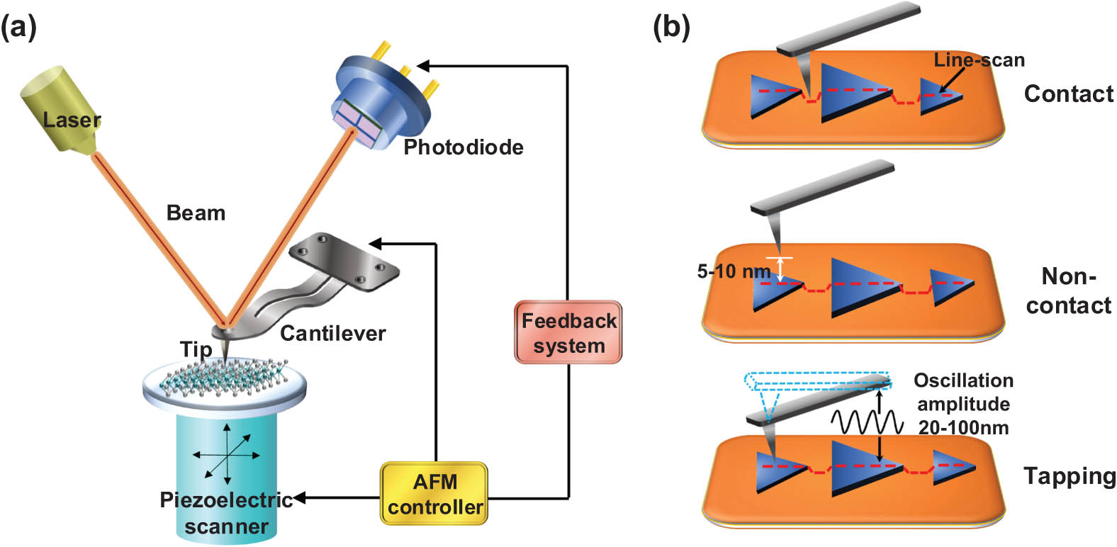
Schematic of a typical AFM setup and its three operation modes. (a) The primary components of a typical AFM setup. (b) Contact, tapping, and non-contact modes of AFM.
Driven by the continued advances in nanotechnology, AFM has evolved from a sensitive imaging tool with unprecedented resolution to a versatile and promising nanofabrication technique. Among the various AFM operation modes developed recently for real-world applications, the contact, tapping, and non-contact modes, as depicted in Figure 1(b), remain the three most fundamental ones. The contact mode, which is the first-ever AFM operation mode and the most commonly used among the three, operates under the action of a constant repulsive force. In this mode, the probe maintains physical contact with the sample surface [44]. As the probe raster scans across the sample surface, the vertical cantilever deflection induced by the sample topography is maintained by an electronic feedback loop with a user preset load force that determines how hard the probe tip pushes against the sample. Along with the gentle or aggressive controlling of the probe-sample interaction, the accurate height or deflection images of samples with a flat or nearly flat surface can be generated via the feedback response. Considering the situations where tip contact may alter the sample and cause damages to the tip or sample, tapping and non-contact modes have been developed, both of which are established on a feedback mechanism of a constant oscillation amplitude. Unlike the non-contact mode with a separation of tens to hundreds of angstroms between the tip and sample surface, the tapping mode operates with the tip intermittently contacting the sample surface and an excited cantilever vibrating at a constant frequency close to its resonance. The tapping mode alternately brings the cantilever tip into the target sample within a minimal amount of time. It appears to be a good compromise between the contact and noncontact modes as it allows for high-resolution topographic imaging with minimum damage to the sample, while maintaining the vibrational properties, such as the frequency, amplitude, and phase of the oscillating tip [45]. The topographical features of the sample and additional information of the surface acquired by any of the three imaging modes or other powerful extensions can properly support the pre-nanofabrication steps, including selecting markers, designing processing routes, and presetting parameters, to ensure that the AFM nanofabrication goes smoothly [46,47].
2.2 Classification of AFM nanofabrication techniques
Due to the operational simplicity, low cost, nanoscale accuracy, and atom-level manipulation capabilities of AFM, AFM probe-based nanofabrication techniques have emerged and experienced significant developments [48]. To initiate and perform the various AFM nanofabrication processes, such as mechanical modification, thermal writing, and local anodic oxidation, the cantilever tip, the central component of an AFM, will be loaded with a vast array of energy and functions as mechanical, heat, electric, and/or chemical sources. According to the dominant tip-sample surface interaction, AFM nanofabrication techniques can be classified as mechanical, thermal, electrical, and other special probe-based techniques (as shown in Figure 2), and their working principles are discussed later in detail [49].
![Figure 2
Classification of AFM nanofabrication techniques. Nanocutting, reproduced with permission from Ref. [50], Copyright © 2020, The Author(s). Nanoindentation, reproduced with permission from Ref. [51], Copyright © 2011, American Chemical Society. Induction of folding, reproduced with permission from Ref. [52], Copyright © 2016, Yi et al. Material modification, reproduced with permission from Ref. [53], Copyright © 2017, American Chemical Society. Material deposition, reproduced with permission from Ref. [54], Copyright © 2014, IOP Science. Thermal indentation and scratching, reproduced with permission from Ref. [55], Copyright © 2021, Liu et al. Electric patterning, reproduced with permission from Ref. [56], Copyright © 2018, American Chemical Society. Local oxidization, reproduced with permission from Ref. [57], Copyright © 2018, American Chemical Society. Electrochemical etching, reproduced with permission from Ref. [58], Copyright © 2022, Han et al. Parallelization, reproduced with permission from Ref. [59], Copyright © 2016, Hirtz et al. Dip-pen, reproduced with permission from Ref. [60], Copyright © 2013, Hirtz et al. Probe performance improvement, reproduced with permission from Ref. [61], Copyright © 2018, American Chemical Society.](/document/doi/10.1515/ntrev-2023-0153/asset/graphic/j_ntrev-2023-0153_fig_002.jpg)
Classification of AFM nanofabrication techniques. Nanocutting, reproduced with permission from Ref. [50], Copyright © 2020, The Author(s). Nanoindentation, reproduced with permission from Ref. [51], Copyright © 2011, American Chemical Society. Induction of folding, reproduced with permission from Ref. [52], Copyright © 2016, Yi et al. Material modification, reproduced with permission from Ref. [53], Copyright © 2017, American Chemical Society. Material deposition, reproduced with permission from Ref. [54], Copyright © 2014, IOP Science. Thermal indentation and scratching, reproduced with permission from Ref. [55], Copyright © 2021, Liu et al. Electric patterning, reproduced with permission from Ref. [56], Copyright © 2018, American Chemical Society. Local oxidization, reproduced with permission from Ref. [57], Copyright © 2018, American Chemical Society. Electrochemical etching, reproduced with permission from Ref. [58], Copyright © 2022, Han et al. Parallelization, reproduced with permission from Ref. [59], Copyright © 2016, Hirtz et al. Dip-pen, reproduced with permission from Ref. [60], Copyright © 2013, Hirtz et al. Probe performance improvement, reproduced with permission from Ref. [61], Copyright © 2018, American Chemical Society.
2.2.1 Mechanical lithography
Mechanical AFM nanofabrication techniques, which were initially invented as a nanometer‐scale lithography in 1992 [62], allow a force to be applied directly to the desired place on the sample surface. During the nanofabrication process, the AFM tip is used as a cutting tool to penetrate or scratch the sample surface. Then, the required force exerted by the tip will either induce the manipulation of the nanoclusters or nanoparticles weakly absorbed onto the surface, or lead to the selective removal of materials from the flat or even curved surfaces, thus forming the pre-designed nanopatterns. The sample can be machined directly by two lithography techniques: static plowing and dynamic plowing, which are derived from the contact and tapping scanning modes, as shown in Figure 3(a) and (b), respectively [63]. Static plowing, also known as scratching, works by applying a constant normal force on the sample surface, which involves a relatively low cost and less workload. In comparison, dynamic plowing is driven vertically by a piezoelectric actuator to provide a lithography technique to modify the sample surface with a vibrating tip at resonance frequency in an arbitrary orientation. This can largely avoid cantilever torsion and further modification of the surface image. When an AFM nanofabrication technique is used to generate nanopatterns, the parameters used to assess the nanofabrication quality, including machining depth, width, and presence of debris pile-up, are closely related to the force applied, cutting velocity, and even the tip structure (construction). For example, the depth of the machining channel generally exhibits a linear and logarithmic relationship with the force applied [37]. Moreover, a deeper machining channel with a larger volume of debris can be fabricated when the cutting velocity is increased [64]. For normal mechanical AFM nanofabrication that does not require any complicated process, machining the grooves directly will inevitably cause pile-up of massive debris and severe damages to the tip. This will in turn lead to an unstable machining process and inaccurate results, thus limiting the further applications of mechanical AFM lithography.
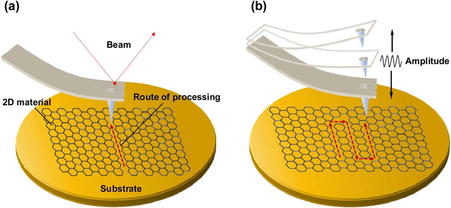
Mechanical nanoscratching by AFM. (a) Static plowing. (b) Dynamic plowing.
2.2.2 Thermal lithography
The first thermal scanning probe lithography (t-SPL) experiment with an AFM tip heated by a focused laser was reported in 1992 for data storage purposes [65]. Over the following decades, t-SPL has developed into a highly versatile nanolithography method that enables accurate and rapid fabrication with a lateral resolution down to 10 nm and writing speeds up to 20 mm/s. To perform thermally induced surface modifications, it is necessary to develop a system that allows for precise scanning on the sample surface, together with a heated tip that can locally activate a nanoscale physical or chemical transformation by Joule heating [66]. Typically, a customized AFM with a piezoelectric fine positioning system is used to scan the sample and mount the thermal probe, as depicted in Figure 4(a). Meanwhile, most AFM-based heaters for standard thermal nanolithography no longer rely on external laser irradiation. Instead, they have been optimized to integrate a combination of a sharp tip and a cantilever with a resistively heated element and will develop further into even more sophisticated components, such as the distance sensor in the Millipede project [67,68]. In t-SPL, heat is the universal stimulus for the functional material modifications. Therefore, temperature, which governs material modification and largely determines the attainable resolution and fabrication speed, is by far the most crucial parameter and should be accurately controlled within the appropriate range. In a resistive AFM-based heater, the tip is heated by a stable current flow or voltage applied on the cantilever legs to a temperature that should be neither too low nor too high. This is because an excessively low temperature will make it impossible to modify the material completely, and an excessively high one will damage the material or reduce the resolution. Due to the complexity of the heat transport from the heater to the sample surface with nanoscale roughness, the effective temperature at the probe–sample interface is different from the heater temperature. It can be challenging to predict the exact value of this temperature, as it is affected by many factors, such as probe geometry, substrate thermal conductivity, sample film thickness, indentation depth, and activation energy. Despite these factors, t-SPL has demonstrated unparalleled precision in nanofabrication. For example, while mechanical lithography can achieve 3D nanostructure fabrication, t-SPL enables even more precise 3D grayscale patterning with a vertical resolution of less than 1 nm. The unprecedented nanofabrication accuracy of t-SPL has recently reestablished itself as a faster and more reliable technical tool, now with an expanded range of applications including the removal, conversion, and addition of target materials [69], as shown in Figure 4(b). However, to fully unlock the potential of t-SPL in the fields of biomedicine, nanomagnetism, and spintronics, several problems still need to be addressed. These include probe wear, difficulty in predicting the accurate temperature at the probe–sample interface, and a lack of a thorough understanding of the heat transfer mechanism.
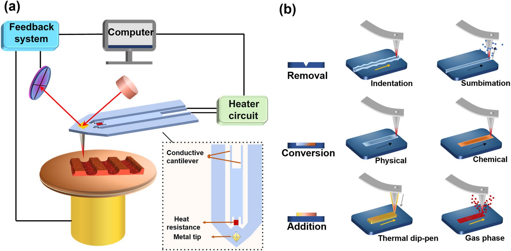
Working principle of AFM thermal processing. (a) Composition of an AFM thermal processing system and the probe structure. (b) Three types of AFM thermal processing: removal, conversion, and addition.
2.2.3 Electric field-induced (EFI) lithography
The EFI SPL has been regarded as a highly attractive tool due to its ability to cause interesting chemical or physical changes on the target sample surface. Compared to its STM counterpart, EFI AFM lithography, which was first developed in 1993 with a conductive AFM tip [70], is more appealing as it enables direct fabrication in an ambient environment [71] and allows selecting an optimum voltage independent of the feedback circuit to achieve high lithography resolution [72]. When short pulses of a moderate voltage (usually from 0 to 20 V) are delivered between the apex of the AFM tip and the sample surface, the exposed surface would be stimulated by an electrical field as high as 108–1010 V m−1 and the associated electron current. This will result in a variety of chemical reactions, deposition of charges or matters, inversion of polarization, or even growth of new materials. Figure 5(a) shows the general working principle of EFI lithography. With a deeper look at the underlying mechanism, the abovementioned chemical or physical changes on the sample surface can be estimated as the consequence of ohmic heating. In this sense, the changes would lead to physical evaporation or desorption in air or vacuum conditions, or electrochemical processes at either the tip or the sample in ambient or liquid environments [73,74]. Among the family of EFI AFM lithography techniques, local oxidation nanolithography (l-OL), known as the most robust and established electrochemical nanolithography method, has been recognized as a highly reliable technology in the nanoelectronics industry. The working principle of l-OL is shown in Figure 5(b), where the AFM tip and substrate are maintained as the cathode and anode, respectively. As the AFM tip approaches the sample surface in contact or non-contact mode, a localized strong electric field within the tip-substrate gap is generated, which will attract ionized water molecules from a humid environment to form a nanoscale water bridge. This will also vertically drive the produced oxygen-containing radicals such as hydroxyl ions from the tip to the sample surface to achieve localized oxide beneath the tip [75]. Typically, the oxidation efficiency is directly related to many operating parameters, such as applied voltage, pulse duration, tip scanning rate, ambient humidity, and substrate cleanliness [76]. Despite their superior patterning uniformity, reliability and diversity, EFI lithography methods, especially l-OL, have relatively low outputs, difficulty in achieving large-area fabrication, and high requirements for the oxidation of the material, which greatly impedes their applicability. Ongoing optimization efforts are being made to explore electric AFM fabrication techniques with higher efficiency and larger areal throughputs to help fabricate more complex 3D nanostructures.
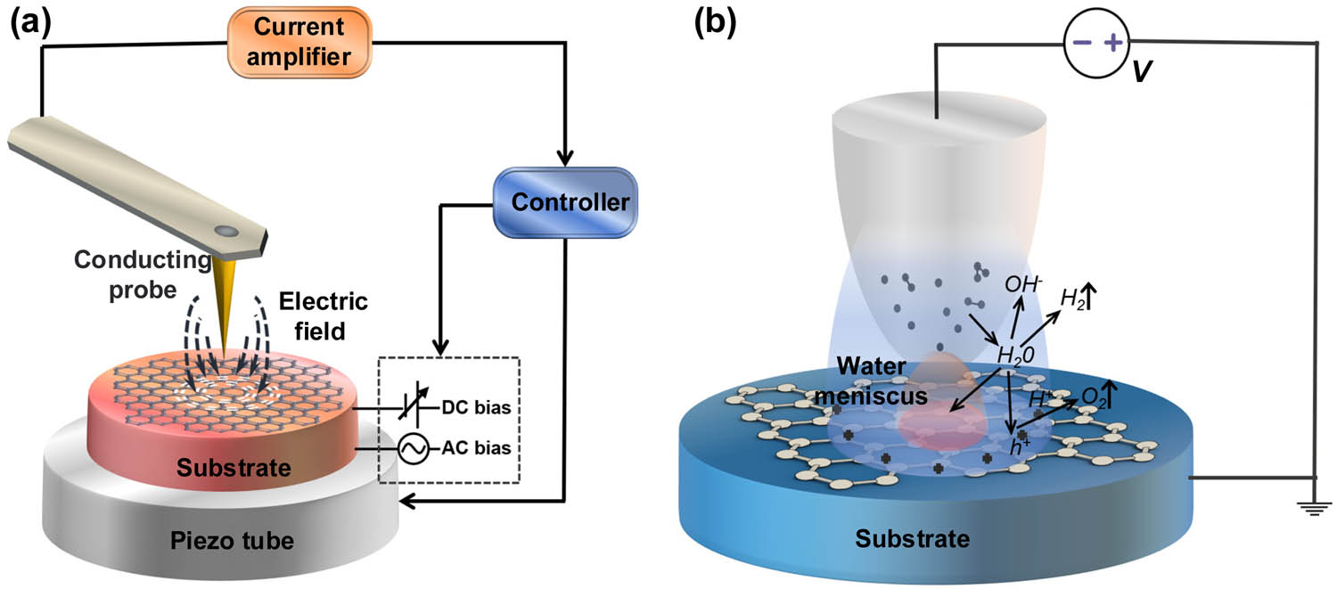
Working principle of AFM electrical nanomachining. (a) The general working principle of EFI lithography. (b) The working principle of l-OL.
2.2.4 Other lithography techniques
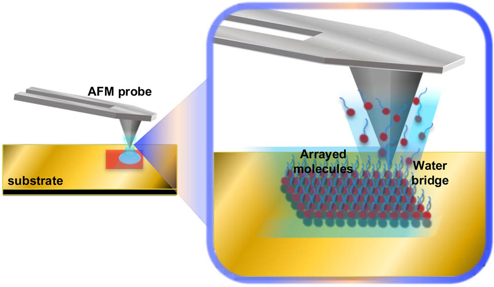
Due to the excellent inclusiveness of the AFM, the abovementioned AFM nanofabrication techniques can be combined with pen dipping, tip modification, parallelization, and other techniques. In this section, we focus on the dip-pen nanolithography (DPN) technique, which has been popular in recent years. The working principle of the DPN technique is shown in Figure 6. Derived from the AFM platform, DPN uniquely combines large areal throughputs, high resolution, good registration, and integration of a broad spectrum of micro- and nano-structured materials. Inspired by the success of additive nanoscale patterning by the AFM [77], DPN, the nanoscale equivalent of writing with a quill pen, was first developed by Rosa LG and his co-workers in 1999 [78]. In the DPN process, a variety of inks, including biological molecules, peptides, colloidal nanoparticles, metal ions, and polymers, are loaded onto the ultra-sharp AFM scanning tip and can be delivered to various substrates upon contact with the surface. Fundamentally, the successful delivery of molecular inks is attributed to the presence of a water meniscus formed between the AFM scanning tip and the substrate. Serving as the transport medium, the water meniscus is either condensed in a suitable humid environment with sufficient water vapor or built up with the ink material itself [79]. In general, the physical transport of the ink diffusion on the AFM tip can be modeled as a three-step process involving dissolution, diffusion, and recombination. This process is influenced by several factors, including surface tension, the chemical and physical properties of the ink and its coverage on the tip, ambient temperature, and humidity, and can be used to guide the prediction of the transport characteristics or the patterned feature size. Thanks to the power of the AFM system, tremendous progress has been made in the DPN technique for the past two decades. It has evolved from a conventional low-throughput single-tip lithography technique to a massive parallel nanofabrication platform with million-pen arrays. This is accompanied by the emergence of more specialized derivatives of DPN. The examples range from cantilever-based DPN techniques with external energy, such as electrical DPN, thermal DPN (tDPN), and mechanical DPN (dip-pen nanodisplacement lithography), to large-area cantilever-free pattering techniques, such as polymer pen lithography, scanning probe block copolymer lithography, hard-tip and soft-spring lithography, and beam pen lithography. All these advances have significantly expanded the applicability of DPN [80].
Working principle of DPN.
In AFM tip-related nanomachining, the AFM tips tend to wear out easily and lose their initial properties quickly after several mechanical or electrical experiments. This can result in unfavorable or even erroneous research results. In this context, in addition to DPN, there has been a notable research focus on exploring the potential of using 2D materials as a protective coating layer for the inner AFM tip. Through the engineering of 2D materials, the ultra-thin nanoflakes can perfectly conform to the intricate profile of the AFM tip, regardless of its geometry. These nanoflakes can be further processed and securely attached to the AFM tip. Moreover, the produced 2D material-coated AFM probes demonstrate several superior properties than those made of solid metals or doped diamonds, such as enhanced mechanical robustness and conductivity, increased resistance to wear, greater levels of hydrophobicity and piezoelectricity, and more versatile surface functionality [81]. Therefore, a series of methods have been proposed to coat AFM probes with 2D materials, including chemical vapor deposition (CVD) growth, CVD transferring, sputtering, liquid phase exfoliation, and thermally assisted mechanical exfoliation [61,82,83]. Notably, the fabrication process of utilizing 2D material-coated AFM tips can involve chemical or physical processes, or a combination of both, which makes this technique considerably more diverse and complex compared to DPN. Hence, in Section 2, we did not delve into the intricate working principle of 2D material-coated AFM tips to the same extent as we did for DPN.
3 Mechanical AFM nanofabrication on 2D materials
Mechanical AFM nanofabrication has proved to be an efficient technique for processing 2D materials [84], such as graphene and its oxide, TMDs, and h-BN, for use in building 2D materials-based electronic devices. Basically, mechanical AFM lithography on 2D materials is achieved through the precise force control of a cutting tool, namely a sharp AFM probe, as covered earlier in Section 2.2.1. According to the specific fabrication results, mechanical AFM nanofabrication on 2D materials is generally divided into three categories: fabrication of localized defects by nanoindentation, partial patterning by nanocutting or nanoscratching, and self-folding with a relatively large areal throughput by mechanical nanomachining [85]. Each of these three techniques can be used to effectively explore and tailor the properties of 2D materials, while providing underpinnings for building high-performance nanooptics and nanoelectronics [86].
3.1 Fabrication of localized defects by nanoindentation
Since the discovery of 2D materials, AFM-enabled nanoindentation, a simple mechanical technique, has been extensively used to investigate the mechanical properties of 2D materials and how they can be used to support the fabrication of flexible devices [87,88]. An AFM-enabled nanoindentation test aims to fully examine the breaking strength and fracture mechanism of 2D materials, which are significant for designing flexible devices. In such a test, localized defects will be induced on the surface of the 2D materials, no matter whether the materials are substrate-supported or suspended. Compared to substrate-supported 2D materials that directly deposit an exfoliated or CVD-grown 2D nanosheet onto the substrate using a transferring method, suspended 2D materials are more complex to prepare. The complexity lies in that the substrate, which is typically made of silicon and covered with a SiO2 layer of a certain thickness, needs to be prepatterned through photolithography, reactive ion etching, or CMOS processing in order to produce the necessary space below the suspended nanosheet [89]. To address this shortcoming, most AFM indentation experiments were performed by puncturing the membrane suspended on the pre-fabricated substrate to ensure that the mechanical properties of 2D materials can be measured accurately. Typically, an AFM probe will be placed at the center of the target microwell, and slowly move downward until nanoscale damages are generated on the surface. Notably, among the considerable AFM nanoindentation experimental studies on 2D materials, we will highlight those that have produced localized defects on the membrane surface, without discussing much about those that emphasize the deformation process with no detectable defects left.
The working principle of AFM indentation on both substrate-supported and suspended 2D materials is shown in Figure 7(a). Useful mechanical information can be extracted from the approaching and retracting motions. Following a pioneering AFM indentation experiment implemented on suspended monolayer graphene nanosheets [90], most of the relevant experiments were designed to be conducted on suspended 2D materials, covering over an array of microfabricated circular holes with diameters ranging from approximately 0.5–3 μm [91,92]. For instance, by indenting the suspended membrane to failure and inducing localized defects on the surface, the breaking strengths of commonly used monolayer 2D materials, i.e., graphene oxide (GO), MoS2, WS2, WSe2,WTe2, h-BN, and black phosphorus, in high vacuum were obtained. The values were 17.3 N/m (24.7 GPa), 15 ± 3 N/m (23 GPa), 47.0 ± 8.6 GPa (29.2 ± 5.3 N m−1), 38.0 ± 6.0 GPa (24.7 ± 3.9 N m−1), 6.4 ± 3.3 GPa (4.5 ± 2.3 N m−1), 8.8 N m−1, and 2.4 ± 1 GPa, respectively [51,93,94,95]. Using a similar method, Lipatov et al. measured the elastic modulus and breaking strength of monolayer and bilayer Ti3C2T x MXene flakes, a relatively new member of the 2D material family [96]. From the fractured membrane, a localized small hole (Figure 7(d)), instead of an extended fracture as in monolayer graphene, was formed on the Ti3C2T x MXene surface, which was ascribed to the larger bending rigidity of Ti3C2T x than graphene [97]. Furthermore, Dai et al. measured the fracture behaviors of boron-doped monolayer graphene [98]. The fabricated defects were penetrated by indentation tips on substitute on dominated graphene, revealing the well-preserved strength and stiffness, and the even more damage-tolerant fracture behavior of heteroatoms-doped graphene. The representative AFM morphologies for fractured graphene, MoS2, and Ti3C2T x MXene are shown in Figure 7(b)–(d). It should be noted that AFM nanoindentation is still prone to some inaccuracies, mainly due to the concentrated stress near the AFM tip along with the crack initiation and insufficient driving force for further crack propagation [99]. In view of this, on the basis of AFM nanoindentation, Zhou et al. systematically investigated the mechanical properties of both substrate-supported and suspended GaTe multilayers, through the combination of full-scale Berkovich-tip nanoindentation, micro-Raman spectroscopy, AFM, and scanning electron microscopy [100]. The experimental results presented an unusual phenomenon that the fractures and cracks are observable for the supported GaTe multilayers but not for the suspended counterparts, revealing a distinct interlayer-sliding and layer-by-layer fracture mechanism.
![Figure 7
(a) Schematic of approaching and retracting motion of the AFM probe in an AFM indentation test on substrate-supported and suspended 2D materials. (b) AFM morphology of a fractured graphene suspended over a microwell, reproduced with permission from Ref. [96], Copyright of © 2018, Alexey Lipatov. (c) AFM morphology of a fractured monolayer MoS2 nanosheet suspended over a microwell, reproduced with permission from Ref. [51], Copyright © 2011, American Chemical Society. (d) AFM morphology of a fractured bilayer Ti3C2T
x
membrane suspended over a microwell, reproduced with permission from Ref. [96], Copyright of © 2018, Alexey Lipatov.](/document/doi/10.1515/ntrev-2023-0153/asset/graphic/j_ntrev-2023-0153_fig_007.jpg)
(a) Schematic of approaching and retracting motion of the AFM probe in an AFM indentation test on substrate-supported and suspended 2D materials. (b) AFM morphology of a fractured graphene suspended over a microwell, reproduced with permission from Ref. [96], Copyright of © 2018, Alexey Lipatov. (c) AFM morphology of a fractured monolayer MoS2 nanosheet suspended over a microwell, reproduced with permission from Ref. [51], Copyright © 2011, American Chemical Society. (d) AFM morphology of a fractured bilayer Ti3C2T x membrane suspended over a microwell, reproduced with permission from Ref. [96], Copyright of © 2018, Alexey Lipatov.
3.2 Partial patterning by mechanical AFM nanomachining
Unlike the fabrication of localized and point-like defects by AFM nanoindentation, partial patterns can be fabricated by mechanical AFM nanomachining on larger surfaces of 2D materials and used as important structural components for building resonators, nanofluidics, or other nanodevices [101]. Such nanomachining can be achieved by contact mode-based static nanocutting and nanoscratching, or tapping mode-based dynamic plowing as described in Section 2.2.1. By having the AFM probe move along the designed paths and carefully adjusting its mechanical pressure applied on the target region, it is possible to generate damages of different shapes, including circles, squares, and ribbons, on the surface of 2D materials [102]. Due to its ease of operation, i.e., requiring no special chemical treatment or resist, mechanical AFM nanomachining is considered suitable for the fabrication of 2D materials, particularly for those sensitive to oxygen and high humidity, such as InGe and GaSe. However, mechanical AFM nanomachining still suffers from the low fabrication quality caused by the unavoidable artifacts, drags, wrinkles, and residual debris generated during the mechanical lithography process, which hinders its use in industrial applications [103]. Considering the characteristics of mechanical nanocutting or nanoscratching, some researchers used this technique to perform nanoscratch tests on the surface of 2D materials so as to investigate the tribological performance of the materials. Other related studies focused on how to improve the quality of mechanical nanoscratching. All these research efforts have demonstrated the significant role played by the AFM nanomachining technique in the study of 2D materials [104].
Performing static contact mode-based AFM nanoscratch tests on 2D materials has been proven to be a feasible method to explore the mechanical response of 2D materials under various conditions and thereby examine their internal mechanical mechanism. In their AFM nanoscratch tests aimed at explaining the underlying mechanism of MoS2 nanosheets of different layers under different scenarios, Özoǧul et al. observed that monolayer MoS2 nanosheets tend to fold and multilayer ones tend to bend [105]. Moreover, Qi et al. figured out the underlying mechanism of the humidity-dependent wear characteristics of graphene [106]. By implementing AFM on various substrates under different levels of humidity, several 1 µm-long lines, with the normal load gradually increased up to 8,936 nN, were fabricated on the surface of the monoatomic graphene layer. Unlike the above single-line AFM nanoscratch experiment, Tran Khac et al. systematically studied the interfacial strength and surface damage properties of a series of 2D materials, including monolayer and multilayer h-BN, MoS2, and graphene atomically thin films, by combining “line scratch” and “area scratch.” The study involved performing AFM-based progressive-force scratch tests with the normal force increasing from 400 to 4,000 nN, and constant-force scratch tests with a defined area of 1 µm × 1 µm under a constant normal force ranging from 500 to 5,000 nN [107]. With a similar hybrid method, Zhao et al. also reported a decrease in friction, namely, the running-in process occurring in monolayer graphene on Cu substrate, by successively performing “line scratch” and “area scratch” tests. The two types of tests are realized by either continuous forward and backward AFM scanning cycles or repeated scratching within a square domain [108] (Figure 8(a)).
![Figure 8
(a) Friction map after a nanoscratch test (obtained under a normal load of 0.130 μN), reproduced with permission from Ref. [108], Copyright © 2020, American Chemical Society. (b) The resulting structure. Colored dots show PL measurement areas, reproduced with permission from Ref. [113], Copyright © 2018, Borodin et al. (c) An AFM image of Z-shaped folded triangular graphene sheets obtained by one-step folding based on AFM nanomechanical folding, reproduced with permission from Ref. [52], Copyright © 2016, Yi et al. (d) An AFM image of a typical MoS2 domain rotated on graphene to achieve a twist angle, reproduced with permission from Ref. [121], Copyright © 2018, Liao et al.](/document/doi/10.1515/ntrev-2023-0153/asset/graphic/j_ntrev-2023-0153_fig_008.jpg)
(a) Friction map after a nanoscratch test (obtained under a normal load of 0.130 μN), reproduced with permission from Ref. [108], Copyright © 2020, American Chemical Society. (b) The resulting structure. Colored dots show PL measurement areas, reproduced with permission from Ref. [113], Copyright © 2018, Borodin et al. (c) An AFM image of Z-shaped folded triangular graphene sheets obtained by one-step folding based on AFM nanomechanical folding, reproduced with permission from Ref. [52], Copyright © 2016, Yi et al. (d) An AFM image of a typical MoS2 domain rotated on graphene to achieve a twist angle, reproduced with permission from Ref. [121], Copyright © 2018, Liao et al.
Through the observations from static contact mode-based AFM nanoscratch tests on the surface of 2D materials, some researchers became aware of the shortcomings of mechanical AFM lithography. To address these shortcomings, they explored ways to improve the quality of mechanical nanomachining on 2D materials, including fewer defects and artifacts on the sample, lower roughness, higher fabrication precision, and fewer debris or residues on the AFM tip. For example, Borodin et al. proposed a frictional mechanical AFM nanomachining method that prevents the cantilever from twisting during the nanomachining process, and allows for repeated lithographic patterning by applying an appropriate pressure on the sample. This method could effectively avoid prominent defects and generate random patterns with a spatial resolution of up to 20 nm on MoSe2 nanoflakes with a thickness of up to 40 nm [109]. Based on conventional mechanical AFM nanomachining, Kun et al. developed a much more precise method for generating patterns on graphene nanoflakes [50]. The method was implemented by first determining the lattice using contact-mode AFM and Fast Fourier Transform filtering and then identifying the zigzag and armchair crystallographic orientations of the graphene flakes. Due to the high symmetry lattice directions for the zigzag and armchair lattice directions, the graphene nanoflakes can be easily cut along the cleavage directions. With this so-called AFM cleavage technique, the precision of the nanofabrication can be significantly improved and the width of the cutting lines can be decreased to approximately 10 nm. Meanwhile, high-quality edges with an average roughness of +/−1 nm were obtained, showing the smoothness of edges fabricated by this method. Apart from the abovementioned improvements made for contact-mode AFM, Shi et al. proposed a novel phase-mode mechanical AFM nanomachining technique for the fabrication of ultra-thin films [110]. Unlike conventional phase-mode AFM plowing techniques that rely on open-loop force control, this method employs the phase response as the feedback signal to realize closed-loop force control, making it particularly suitable for materials with a thickness below 10 nm, such as polymer thin films, metallic thin films, and 2D materials. Due to the insensitivity of the phase response to the piled-up debris, the phase-mode mechanical AFM nanomachining technique can largely eliminate the debris effect and avoid severe tip wear, thus realizing highly precise fabrication. Li et al. utilized the ability of this technique to monitor the phase response in real time to fabricate monolayer and multilayer MoS2 nanosheets in a layer-controllable manner. This demonstrates the superiority of closed-loop phase-mode mechanical AFM nanomachining over its conventional counterparts [111].
Although mechanical AFM lithography is still in its infancy, some researchers have utilized mechanical AFM nanomachining as an effective lithography technique to fabricate desired structures for nanodevices. For instance, to build all-carbon field-effect transistors (FETs), Xie et al. utilized an AFM-based mechanical cutting method to fabricate assembled graphene nanoflakes into nanoribbons and interdigitated electrodes which serve as the source and drain of the FETs. After evaluating the electrical properties of graphene nanoribbons (GNRs) with line defects, pristine graphene was fabricated into two interdigitated electrodes with a nanogap width of 94 nm according to the designed machining path [112]. Moreover, as reported by Borodin et al., resonators, the basic component of many nanophonic devices, can be fabricated via mechanical AFM nanomachining [113]. By determining the proper pressure force through a dozen of lithography iterations, reflecting the degree of the interaction between the AFM probe and the nanoflake, a few hundreds of lithography iterations were conducted to generate the desired resonator structure with the designed shape and size. Then, a circular ring-shape nanophotonic structure (Figure 8(b)) with a diameter of 1,500 ± 30 nm and a gap width of 900 nm was generated on the multilayer MoSe2 nanoflake with a thickness of 70 ± 2 nm. The relevant optical measurements have shown the evident resonance of the created structure, demonstrating the potential of mechanical AFM lithography in fabricating nanophotonic devices.
3.3 Folding and rotation by mechanical AFM manipulation
It is known that applying external driving forces on thin films can cause them to bend, delaminate, crack, or even fail, which keeps them from depositing. However, applying external driving forces may be a feasible way to engineer atomically thin films, such as 2D materials, as their optical, mechanical, electronic, and magnetic properties are all highly customizable. With exceptional bending stiffness and strong in-plane rigidity, 2D materials can be folded and rotated to a certain angle by mechanical AFM manipulation, such as cutting torsion, traveling wave excitation released during AFM scanning, and load force pushing. This folding and rotation technique provides an effective alternative for the creation of more complex layered or twisted structures. Specifically, flat 2D nanosheets can be constructed into promising applications in various engineering fields, including energy storage, biosensors, 3D optics, and superconductive electronics [114,115,116,117].
Generally, the folding construction of atomically thick 2D materials is a self-driven process. This means that the folding configuration will not stabilize until an energy balance is reached between two involved layers. Therefore, how the folding process goes is closely related to the geometric parameters of the structure. For the folding events of 2D materials initiated by AFM tip-based mechanical manipulation, the sample should be prepared by mechanical exfoliation in advance, and the folding process largely relies on the precise force control and skillful manipulation. Despite these drawbacks, AFM tip manipulation has been widely used as a reliable folding method for 2D materials. As one of the most representative 2D materials with an exceptionally high in-plane Young’s modulus, graphene has been extensively investigated in folding and bending experiments. Using the repetitive contact-mode mechanical AFM nanomachining, Rode et al. fabricated a set of 16 self-assembling folded nanoribbons with lateral sections connected to the mother flakes [118]. Furthermore, they made a thorough analysis of an unexpected correlation between the geometrical parameters of the folded structure and the nanoribbon width. Similarly, using the AFM technique to initiate a self-driven folding process for monolayer graphene nanosheets, Bockhorn et al. found that the formation and dynamic evolution of one-cut structures are vastly different from those of two-rip structures, which was attributed to the conservation of energy in searching for efficient configurations [119]. Besides the normal contact-mode AFM nanomachining, Yi et al. utilized the lateral force mode AFM nanomachining to realize stable z-shape folding conformation of flat graphene sheets (Figure 8(c)) [52]. Moreover, Chang et al. proposed a unique AFM nanomachining technique to generate self-folding by multiple cycles of contact-mode AFM scanning along an arbitrarily chosen scan line with an intentionally applied force. The folding event was attributed to the transmission of sufficient energy by the tip-induced traveling wave to overcome substrate adhesion [120].
Studies on the rotation of 2D materials focus on the rotational angle adjustment by employing the alterable electronic properties of 2D materials and heterostructures to adjust the angle between layers. Given the weak van der Walls force between the atomic planes of 2D materials, AFM tip-based mechanical manipulation can be utilized to precisely control the twist angle, thereby adjusting the angle-dependent properties of 2D materials. With this technique, Liao et al. experimentally investigated the angle-dependent conductivities of MoS2/graphene heterostructures. By controlling the movement of the AFM tip along the corner of MoS2, MoS2 domains were rotated on graphene substrate with any twist angle, as shown in Figure 8(d) [121]. For the same MoS2/graphene heterostructures, Yuan et al. demonstrated an ultra-precise AFM tip manipulation method to control the interlayer twist angle. During the experiment, with MoS2 sheets pinned at graphene boundaries, graphene wrinkles were utilized as the fulcrum of the rotation process to offer an extra force for precise rotation control [122]. In addition, Ribeiro-Palau et al. developed an in situ AFM tip controllable rotation method for BN/graphene/BN heterostructure devices with dynamically twisted layers. By rotating the arms of the uppermost pre-shaped BN structure with an AFM tip, the top layer of the devices can be adjusted to any desired angle [123].
4 Thermal AFM probe nanofabrication on 2D materials
As an eye-catching member of the large SPL family, t-SPL has been widely applied to 2D materials due to its nanometer-scale and microsecond timescale precise patterning and unique direct writing capabilities [124]. With a heated nanotip based on AFM, or a more complex integrated system originating from AFM as described in Section 2.2.2, continuous indentation can be achieved to create nanopatterns with greyscale resolution on the surface of 2D materials. Unlike the commonly used EBL technique, t-SPL can avoid electron-induced damages on 2D materials. Meanwhile, t-SPL can be implemented under atmospheric operational conditions, and has a maskless, cost-effective nanopatterning capability that provides comparable throughput to EBL. Additionally, t-SPL supports closed-loop lithography, which allows the sample to be indented continuously by the heated nanotip and at the same time be scanned by the cold nanotip.
According to the thermal nanofabrication process on 2D materials, t-SPL can be divided into two parts: the indirect polymer film lithography which defines the target region, and the one-step direct writing lithography on 2D materials, which will be discussed in detail in Sections 4.1 and 4.2.
4.1 Indirect polymer film lithography
Generally, the nanopatterning of 2D materials by t-SPL consists of two steps: the initial patterning of the organic resist previously deposited on 2D materials through the localized evaporation of the heated probe, and the subsequent transfer of patterns onto the material surface via ion or plasma etching. t-SPL can not only cause metal electrodes to be deposited on the target region of 2D materials but can also aid in producing desired 2D materials.
To produce graphene-based FETs with high performance, Zheng et al. applied the t-SPL technique to pattern high-quality metal electrodes on the surface of a wide range of 2D materials, including monolayer MoS2, WSe2, and exfoliated h-BN nanoflakes, to form top-gated and back-gated FETs [125]. Prior to the electrode patterning, the 2D material was spin-coated with two layers of polymer films, which served as the thermal sensitive top layer and the sacrificial bottom layer. After selective removal of the polymer layers by t-SPL with lateral resolutions of less than 10 nm and vertical resolutions of 1 nm, the contact region prepared for metal deposition was patterned on the MoS2 or WSe2 surface, respectively. Subsequently, metal electrodes with sub-10 nm resolution, high reproducibility, and high throughputs were produced on the target region of the 2D material by t-SPL. Due to its high accuracy and harmlessness, t-SPL has been successfully applied to the fabrication of high-performance electronic devices based on a wide range of 2D materials.
To accommodate next-generation 2D material-based applications, it is crucial to build 2D materials with customized high-resolution geometries so as to bring their appealing properties into full play. Therefore, besides the t-SPL-assisted fabrication of electrodes on 2D materials, there have also been studies in which t-SPL is used to fabricate 2D materials themselves into finite structures. To investigate the capabilities and limitations of t-SPL in patterning, Maaskant employed t-SPL to achieve precise grayscale patterning of h-BN [126]. By locally evaporating the organic resist through the heated probe of t-SPL, the pattern written into the resist was subsequently transferred onto the h-BN nanoflakes. They successfully obtained a series of square hole arrays and patterns of different depths with a minimum feature size in the fractal pattern with a full width at half maximum (FWHM) of 40 nm (40 nm in pattern depth) on the exfoliated h-BN nanoflakes.
To go beyond the application of t-SPL in the fabrication of either metal electrodes or 2D materials themselves, Liu et al. successfully combined these two parts of fabrication on graphene [127]. They managed to produce graphene-based FETs processed entirely by t-SPL. Figure 9(a) and (b) show the model diagram and optical image of the device, respectively. Similar to the fabrication technique reported by Zheng et al. [125], a two-layer polymer stack resist was used for the patterning process, which involved the initial thermal decomposition performed by t-SPL, and the subsequent oxygen plasma etching. In this way, both an active region with an FWHM of 10–16 nm and high-quality metal electrodes with a minimum channel length of 60 nm were created on the target region of monolayer graphene. This demonstrates that the technique provides a powerful approach to the fabrication of high-performance graphene-based FETs.
![Figure 9
(a) The optical image of the graphene-based FETs, reproduced with permission from Ref. [127], Copyright © 2021, Liu et al. (b) The optical image of a backgated graphene device after lift-off, reproduced with permission from Ref. [127], Copyright © 2021, Liu et al.](/document/doi/10.1515/ntrev-2023-0153/asset/graphic/j_ntrev-2023-0153_fig_009.jpg)
4.2 Direct writing
Direct writing thermal lithography, an alternative to the indirect t-SPL lithography that relies on polymer patterning for nanofabrication, has been realized by several researchers. Instead of spin-coating organic materials on 2D materials for pattern transfer, the nanotip was directly applied onto the 2D nanoflakes to produce the desired shapes or sizes. Generally, there are diverse options for the nanotip used for the direct writing of 2D materials, as it can be either a specially treated AFM tip, or the direct writing head of an integrated thermal lithography instrument [53].
Using a heated AFM tip at varying temperatures and writing speeds in contact mode AFM, Lee et al. reported a novel technique that combines thermal and chemical lithography to fabricate GNRs [128]. Figure 10(a) illustrates the indentation caused by probes at different temperatures. By controlling the movement of the heated AFM probe, highly insulating graphene fluoride was transformed and locally converted into conductive graphene under inert environments. The GNRs fabricated with this technique have a width adjustable from 40 to 200 nm, and their conductivity can be adjusted by altering the gas mixture component. With a similar method, Raghuraman et al. locally cleaved oxygen groups from GO and performed surface chemistry measurements on the fabricated GNRs, as shown in Figure 10(b) [129].
![Figure 10
(a) Sequentially written 250 × 500 nm rectangles with the probe held at different temperatures, reproduced with permission from Ref. [128], Copyright © 2013, American Chemical Society. (b) The schematic of reduction by a heated tip, in which oxygen groups are removed with pressure and heat, reproduced with permission from Ref. [53], Copyright © 2017, American Chemical Society. (c) AFM topography map of nanosquare arrays in monolayer MoTe2, reproduced with permission from Ref. [55], Copyright © 2021, Liu et al.](/document/doi/10.1515/ntrev-2023-0153/asset/graphic/j_ntrev-2023-0153_fig_010.jpg)
(a) Sequentially written 250 × 500 nm rectangles with the probe held at different temperatures, reproduced with permission from Ref. [128], Copyright © 2013, American Chemical Society. (b) The schematic of reduction by a heated tip, in which oxygen groups are removed with pressure and heat, reproduced with permission from Ref. [53], Copyright © 2017, American Chemical Society. (c) AFM topography map of nanosquare arrays in monolayer MoTe2, reproduced with permission from Ref. [55], Copyright © 2021, Liu et al.
Besides thermal-assisted chemical transformation on 2D materials with a heated AFM tip, direct writing on the surface of 2D materials by t-SPL has also been achieved by means of thermomechanical indentation. Liu et al. reported precise results for the direct thermal cutting of 2D materials of various geometries [55]. Using a heated nanotip for local thermomechanical cleavage of the chemical bonds of 2D materials under ambient pressure and temperature, they obtained nanoribbons, nanosquares (Figure 10(c)), or other arbitrary nanopatterns with a resolution of 20 nm on monolayer MoTe2, MoS2, and MoSe2. As part of the process, 2D materials were transferred onto the polymer layer. Then, the chemical bonds of the 2D layer were initially broken by a force applied on the nanotip, and further deepened by sublimating the polymer below the 2D layer. The combined use of heat and indentation in this study was apparently different from the mechanical AFM nanofabrication techniques discussed earlier. With the same technique, Liu et al. also created strain nanopatterns on 1-layer and 2-layer 2D TMDs and monolayer graphene [130]. Beyond the simple breakage of the 2D layer in [55], they obtained well-controlled local deformations, such as lines, squares, or even ripples with adjustable depth, on 2D materials by adjusting the parameters, such as the indentation force and tip temperature. This study revealed a promising method for precisely tuning the bandgap of 2D materials.
5 EFI AFM nanofabrication on 2D materials
When an electric field, instead of a thermal AFM probe, is used in t-SPL, another branch of SPL termed as EFI AFM lithography comes into being. EFI AFM lithography has been recognized as an appealing bias-assisted tool due to its ability to create versatile functional groups or new materials on the target materials. Recently, the advanced EFI technique has emerged as a low-cost, maskless, high-resolution, high-speed, and high-throughput method for electron-induced nanomanufacturing [131]. With these features, EFI can be used for property modulation and localized modification of 2D materials, including deposition, transformation, desorption, or large-area nanopatterning. In general, EFI AFM on 2D materials is relatively simple and clean, as it does not require using any polymer resist and leaves no sacrificial residues on the material surface. With spatial resolution down to the atomic scale, EFI AFM lithography can achieve localized modification on surface, lateral patterning, or even layer-by-layer thinning for 2D materials. More details about these capabilities will be provided in Sections 5.1 and 5.2 [132].
5.1 Property alteration and modulation by an AFM-induced electric field
By applying an electric field on 2D materials via AFM or other AFM-based electrical techniques, we can not only acquire the essential information of 2D materials through electrical measurements, but also modify or modulate their properties using electrical lithography methods. In this review article, we choose not to discuss EFI property characterization which is commonplace in studies on 2D materials or the use of conductive AFM to purely perform electrical measurements on 2D materials. Instead, we focus on AFM nanofabrication techniques that involve electrochemical processes for the alteration or modulation of the electrochemical and frictional properties of 2D materials.
As an attractive nanofabrication technique, AFM-induced electric field nanolithography can trigger a variety of chemical changes based on the electrochemical reactions taking place on the target semiconducting or metal materials. As for 2D materials, diversified electrochemical products at the specific locations of the material surface can be obtained and their electrochemical properties can be reasonably influenced or modulated under an AFM-induced electric field. For example, Liu et al. proposed a method in which a negative bias voltage is applied with an AFM tip to induce the electrochemical functionalization of graphene as oxygen-containing functional groups attached on the graphene surface [133]. Moreover, as reported by Zou et al., under the action of an AFM tip bias-induced electric field, localized hydrogen ions can be produced in the vicinity of 2D α-MoO3 nanoflakes at ambient environments, and then intercalated into its lattice. This results in the generation of H+ as well as an evident shrinkage of the bandgap and changes in the electrical behavior [134].
Besides the electrochemical properties, many studies have been conducted recently to examine the modulation of the frictional properties of 2D materials, which is closely related to the EFI electrochemical process. Several mechanisms underlying the modulation of frictional properties have been proposed, including sliding-related electron motion, electrostatic forces, and photo vibration. These mechanisms also apply to 2D materials. Based on these theoretically established mechanisms, the tunable frictional behavior of a series of 2D materials, including graphene, h-BN, and MoS2, have been preliminarily investigated via a biased AFM tip. For instance, using a high-resolution and small-size AFM tip, Lang et al. electrochemically functionalized monolayer graphene deposited on an insulating substrate along with the decomposition process of water molecules [135]. They also realized tunable functionalization for this material by changing the applied negative voltage, which is determined by both the stable time and the potential difference between the AFM tip and graphene. Furthermore, they observed about an 8-fold increase in friction with the increase in the voltage of the tip, which could enable higher levels of functionalization for the material. This phenomenon was attributed to the combination of the EFI meniscus force and electrostatic force. To take a step away from applying a negative voltage alone, in a recent work by Lang et al. [136], both positive and negative bias voltages were applied to comprehensively investigate the atomic scale friction, as shown in Figure 11(a). The results showed that the friction increases as the applied voltage increases and the friction under the positive bias voltage is lower than that under the negative one (Figure 11(b)). The different friction responses were attributed to the different inherent functions and the water molecules between the tip and graphene. Yu et al. conducted a similar study to explore the nanofriction characteristic of h-BN. They observed distinct friction behaviors of the material under positive and negative bias voltages, which was attributed to the electrostatic interaction caused by the charging effect [137]. Shi et al. set their sights on the atomically thin MoS2 by experimentally and theoretically investigating the material’s friction behavior under a negative electric field induced by an AFM tip [138]. The average friction force of the MoS2 sheet varies with the normal load at different grid voltages. The material experienced nearly a 5-fold decrease in friction, which could constitute an ultra-low friction state and was attributed to the electronic tight binding between the material and the substrate. To better understand the origin of friction on an electronic level for 2D material interfaces, Song et al. studied the atomic-scale friction at the interface between the AFM tip and graphene by applying an electric current induced by conductive AFM [139]. They observed the tuning of friction as the electric current was applied. They provided an adequate explanation of this observation through a model that takes into account the electron transfer-induced potential energy change and the interaction energy. The model depicted in Figure 11(c) was established to support their findings. The model is expected to be applicable for a variety of tribosystems, including the interfaces of 2D materials.
![Figure 11
(a) Schematic of current-carrying friction measurements, reproduced with permission from Ref. [136], Copyright ©2020, American Chemical Society. (b) Adhesion at different tip voltages to show the difference in adhesion at positive and negative bias voltages, reproduced with permission from Ref. [136], Copyright ©2020, American Chemical Society. (c) Schematics of the electronic property fluctuation model, reproduced with permission from Ref. [139], Copyright © 2022, American Chemical Society.](/document/doi/10.1515/ntrev-2023-0153/asset/graphic/j_ntrev-2023-0153_fig_011.jpg)
(a) Schematic of current-carrying friction measurements, reproduced with permission from Ref. [136], Copyright ©2020, American Chemical Society. (b) Adhesion at different tip voltages to show the difference in adhesion at positive and negative bias voltages, reproduced with permission from Ref. [136], Copyright ©2020, American Chemical Society. (c) Schematics of the electronic property fluctuation model, reproduced with permission from Ref. [139], Copyright © 2022, American Chemical Society.
5.2 Nanopatterning by l-OL
As the most common EFI AFM lithography technique, l-OL has led to a renewed interest in the fabrication of 2D materials. This technique can be used to nanofabricate any type of 2D material. It uses a conductive AFM probe coated with metals, such as Au, Pt, and W, to induce a series of electrochemical reactions between the probe and the material surface, thereby causing changes in the material surface. As a result, a broad variety of chemical products, including oxides and other derivatives, will be generated above and below the material surface, which varies with the operating conditions, such as bias polarity, DC/AC driven current, or gas composition. In most cases, the generated oxides can be easily removed by water to allow in situ patterning of 2D materials. Therefore, l-OL has been widely used in the EFI AFM lithography-based nanofabrication of 2D materials and has achieved remarkable results. We will discuss more about this technique next.
As a representative 2D material, graphene, along with its oxide, has been the focus of many studies on EFI AFM lithography. Using conductive AFM, Seo et al. created locally reduced GO nanopatterns on GO nanosheets [140]. With a negative bias voltage applied on the n-doped Si substrate, p-type reduced GO nanolines with an average FWHM of 25 nm were produced, exhibiting a higher conductivity than their chemically prepared counterparts. With a similar method, Zhang et al. utilized a Pt-coated AFM probe to locally catalyze the reduction reaction of GO in an atmosphere rich with hydrogen [141]. By creating nanoribbons with resolution of approximately 20 nm (Figure 12(a)), they successfully fabricated prototype ambipolar FETs on arbitrary substrates under mild operating conditions. Different from the above reduction process, Liou and Woon investigated the oxidation process of graphene by oxidation SPL [142]. With a negative bias voltage, which ranged from −10 to −8 V and came with a controllable pulse duration of 10 ms, applied on the metallic AFM tip in contact mode, circular ring-like trenches (Figure 12(b)) were patterned on the CVD-grown graphene. The size of these trenches increased with the increase in the bias voltage and relative humidity. Based on the mechanism for the formation of oxidation SPL patterns, which was established both experimentally and theoretically, Quesada et al. successfully fabricated high-quality and large-area GO [143]. Notably, the large-area local anodic oxidation in this study was performed using a special instrument developed from the basic contact and tapping modes of AFM, which enabled high-speed and scalable production of oxidized regions. With this instrument, monolayer GO regions with any size from micrometers to unprecedented mm2 can be generated in just a few minutes. Besides silicon substrates, Alekseev et al. also reported a local anodic oxidation method to generate GP regions on SiC substrates. With this method, they obtained a GNR with a width of 20 nm and a record-breaking graphene nanoconstriction between the oxidized regions with a width of 10 nm [144]. Meanwhile, graphene and its oxide can also be combined with other 2D materials to fabricate more complex electronic devices. For example, Du et al. utilized oxidation SPL to establish a seamless 2D-based device with an aim to overcome structural defects and polymer residues [145]. In the fabricated MoS2 FET with the channel 1 μm in length and 8.5 μm in width, graphene and its oxide served as the electrodes and the intermediate part between the two electrodes, respectively.
![Figure 12
(a) AFM topography of nanoribbons, reproduced with permission from Ref. [141], Copyright © 2012, Zhang et al. (b) Topographical mapping of the area at different voltages and humidities, reproduced with permission from Ref. [142], Copyright © 2019, American Chemical Society. (c) An AFM image of a GNR array prepared by EFLAO, reproduced with permission from Ref. [56], Copyright © 2018, American Chemical Society.](/document/doi/10.1515/ntrev-2023-0153/asset/graphic/j_ntrev-2023-0153_fig_012.jpg)
(a) AFM topography of nanoribbons, reproduced with permission from Ref. [141], Copyright © 2012, Zhang et al. (b) Topographical mapping of the area at different voltages and humidities, reproduced with permission from Ref. [142], Copyright © 2019, American Chemical Society. (c) An AFM image of a GNR array prepared by EFLAO, reproduced with permission from Ref. [56], Copyright © 2018, American Chemical Society.
Apart from graphene, atomic TMDs have attracted interest from many researchers due to its inherent bandgap and promising optical and electrical properties. The relevant research efforts have been focused on how to fabricate devices out of TMD flakes, especially with the aid of the simple and resist-free oxidation SPL. For instance, Fernandes and Gadelha proposed a technique to nanofabricate monolayer-thin islands on few-layer and bulk MoS2 via oxidation SPL. The fabricated islands were buried underneath the molybdenum oxide [146]. It remains to be investigated whether the technique is capable of creating monolayer regions of any desired size, shape, and resolution by adjusting the applied bias, dwell time, and relative humidity. Despite this, the produced oxides presented dramatically increased PL intensity, demonstrating that the technique offers a promising approach to the fabrication of high-performance 2D optoelectronic devices. With a similar oxidation SPL technique based on AFM, Zhao et al. investigated the key parameters influencing the patterning of monolayer TMDs, including MoS2, MoSe2, WS2, and WSe2 [147]. A thorough comparison of the parameters revealed that the dwell time of the tip plays an important role in achieving thickness-controllable oxidation. It was also reported that sub-100 nm patterning resolution can be achieved by tuning the applied voltage bias, amplitude setpoint, and relative humidity. To further improve the nanopatterning resolution of oxidation SPL, Dago et al. combined oxygen plasma and AFM-based oxidation SPL to define nanoscale patterns on the surface of WSe2 nanoflakes [57]. The pre-treatment by oxygen plasma induced p-type doping underneath the WSe2 layer. More importantly, the width and depth of the fabricated nanoribbons can be controlled properly. The combined fabrication process resulted in an array of ten oxide nanowires with a half-pitch of 36 nm and a nanoribbon-based WSe2 FET with an array of five parallel 350 nm half-pitch nanoribbons. Using the same fabrication process, Ryu and Dago produced sub-10 nm nanoconstrictions and nanoribbon-based FETs on few-layer MoS2 and MoSe2 [148]. Prior to the oxidation SPL process, a uniform oxide layer with a thickness of 3–4 nm was formed on the surface of the MoX2 flake, which can screen the underlying nanoflake and enable nanopatterning with good control of the shape and size.
Oxidation SPL has also been used in the nanopatterning of other 2D materials such as black phosphorus and h-BN. Liu et al. proposed a technique for the nanopatterning and layer-by-layer thinning of black phosphorus by formation of oxidized phosphorus species [149]. Besides using a DC bias for the nanopatterning and thinning of black phosphorus on conductive substrates, the technique also used an AC bias, along with varying parameters, to enable the nanopatterning and thinning of this material on commonly used dielectric substrates, which greatly broadened its applicability. Focused on the electrode-free oxidation SPL driven by pure AC through capacitive coupling, Li et al. demonstrated a flexible and high-precision method for the nanopatterning of graphene, h-BN and other low-dimensional materials [56]. Figure 12(c) shows the AFM image of a GNR array prepared by EFLAO. With the appropriate AC parameters used, the technique can achieve nanopatterning with 10 nm resolution on a series of 2D materials without pre-treatment or pre-fabrication of the contacting electrode, demonstrating its suitability for the fabrication of other nanomaterials.
6 Other techniques for AFM nanofabrication on 2D materials
This section covers some other techniques for the AFM tip-related nanofabrication of 2D materials: DPN and 2D material-coated AFM tips. Notably, the fabrication by 2D material-coated AFM tips can involve chemical or physical processes, or the combination of both, which means this technique is much more diverse and complex than DPN. Therefore, we did not go into details on the working principle of 2D material-coated AFM tips in Section 2 as we did for DPN. Instead, we have singled out Section 6.2 for a detailed discussion about 2D material-coated AFM tips.
6.1 DPN
As covered earlier in Section 2.2.3, DPN has evolved from a simple printing technique that relies on an AFM tip to a versatile technique that enables nanofabrication with high spatial resolution, low costs, and broad applicability for materials including 2D ones. Notably, the cantilever-free derivatives of DPN for 2D material nanopatterning are not covered here in our review since they are unrelated to AFM tips. According to the actual application, the results of DPN on 2D materials via AFM tips or more sophisticated AFM tip-based instruments can be divided into several categories, including etch resist patterns, biological structures, or chemical templates on the surface of pre-deposited 2D materials, and direct construction and assembling of 2D materials.
DPN can flexibly produce microscale or nanoscale patterns with tunable feature sizes and a resolution of sub-50 nm. Such patterns can be further used to make etching masks or resists to assemble functional devices. For example, using a basic dip-pen technique, Kim et al. fabricated GNR electrodes on a SrTiO3 substrate to form a resistive switching memory device [150]. Prior to the DPN process, monolayer graphene was mechanically exfoliated onto the SrTiO3 substrate. Then, a 50 nm-wide polystyrene nanorod was printed by DPN to serve as the etching mask to fabricate GNR electrodes with a gap of 30 nm, which can be used to form a SrTiO3 substrate-based resistive switching device. In contrast to the fabrication by using a tip with a certain speed, Chen et al. presented a controllable DPN technique to deposit constricted polymer structures on the surface of monolayer MoS2 for building MoS2 nanoribbon FETs (Figure 13(a)) [151]. Upon the CVD growth of monolayer MoS2 onto SiO2/Si substrates, tDPN was performed with a solid ink “direct writing” onto the MoS2 and substrate surface. Using a heated AFM tip whose temperature was kept within 210–300℃ and speed within 100–1,000 nm/s, the deposition of the polymer mask was well adjusted to allow tailoring the width of the fabricated narrow lines.
![Figure 13
(a) Schematic of the fabrication of a single-layer MoS2 nanoribbon FET, reproduced with permission from Ref. [151], Copyright © 2019, American Chemical Society. (b) Proposed membrane organization on graphene, reproduced with permission from Ref. [60], Copyright © 2013, Hirtz et al. (c) Parallel DPN cantilever arrays transfer different lipid mixtures onto graphene squares, reproduced with permission from Ref. [59], Copyright © 2016, Hirtz et al.](/document/doi/10.1515/ntrev-2023-0153/asset/graphic/j_ntrev-2023-0153_fig_013.jpg)
(a) Schematic of the fabrication of a single-layer MoS2 nanoribbon FET, reproduced with permission from Ref. [151], Copyright © 2019, American Chemical Society. (b) Proposed membrane organization on graphene, reproduced with permission from Ref. [60], Copyright © 2013, Hirtz et al. (c) Parallel DPN cantilever arrays transfer different lipid mixtures onto graphene squares, reproduced with permission from Ref. [59], Copyright © 2016, Hirtz et al.
Thanks to AFM tip-assisted DPN, a diverse set of biomolecules and chemical templates have been directly or indirectly immobilized into 2D materials for specific functionalization. As the most commonly used biomolecules for improving the function of 2D materials, biomimetic lipid membranes can be patterned efficiently by DPN in a highly controllable and parallel manner. Since Hirtz et al. proposed the direct assembling of tailored lipid membranes on graphene, phospholipids have been proven to exhibit higher mobility on 2D materials compared to other commonly used substrates [60]. This has in turn aroused enthusiasm among researchers to explore, both experimentally and theoretically, lipid DPN techniques for graphene and other 2D materials. For instance, Hirtz et al. implemented top-down and self-assembly of large-area phospholipid membranes in arbitrary shapes on the CVD-grown monolayer graphene (Figure 13(b)) after the successful fabrication of lipid patches on graphene [59]. With a multi-cantilever array, membrane patches with an area of 1 × 1 mm2 and a 100 μm pitch were patterned within 0.5 min, as shown in Figure 13(c), much faster than fabrication by typical lipid DPN. Moreover, graphene or GO-supported lipid membranes were investigated by simulations and experiments to explore the dynamical properties of the lipid-graphene/GO interactions [152]. The simulation and experimental results were found to be consistent, which demonstrated the importance of the surface polarity and solvent environment while offering valuable guidance for the future application of graphene and GO in biotechnology. In addition to the biological structure, prototypical chemical templates have been used to locally modify the properties of the surface of the target 2D materials. For example, Zhou et al. used DPN to immobilize rhodamine-based dye molecules (Rhodamine 6G, R6G) with a controllable size on graphene [153]. Through a typical dip-pen experiment using an AFM tip with varying writing speeds and pre-coated with 1 mM R6G ink, an array of R6G lines with variable widths were directly written on the exfoliated graphene. In contrast to the results from conventional dip-pen experiments, the produced array of R6G lines basically exhibited constant widths that were irrelevant to the writing speed. This was possibly attributed to the effective tip size or the water meniscus formed between the tip and substrate. However, when the R6G ink was depleted, the width of the produced lines was observed to depend significantly on the writing speed. After identifying the assembly properties of R6G at high or low concentrations, the researchers conducted further experiments to verify the electrical behaviors of graphene locally modified by R6G molecule patterning. This suggested the possibility of locally and quantitatively n- or p-doping graphene with DPN-pattern R6G.
6.2 2D material-coated AFM probes
As covered in Section 2.2.4, various techniques such as CVD growth, CVD transferring, sputtering, liquid phase exfoliation, and thermally assisted mechanical exfoliation have been employed to fabricate 2D material-coated AFM probes. The aim of these techniques is to enhance the properties of the probes beyond those made of solid metals or doped diamonds. These fabricated AFM probes have shown great potential in many real-world applications, including electrical characterization [154], low-friction and low-stiction micro- and nanoelectromechanical systems (MEMS and NEMS) [155,156], bio-MEMS [157], micro/nanomachines [158], molecular electronics [82], and even nanopatterning of 2D materials via controllable AFM probe exfoliation [159].
There has been a growing trend where the conventional CVD technology, which can be used to produce large-area and continuous 2D nanofilms, is combined with the transferring method to fabricate 2D material-coated AFM probes, especially graphene-coated nanoprobes. For example, based on the CVD growth method, Lanza et al. [154] and Martin-Olmos et al. [160] successfully transferred a single layer of continuous graphene film onto the AFM tips using PMMA-assisted and Cu mold-assisted transferring methods, respectively. Figure 14(a) shows the AFM tip obtained by copper-substrate-assisted transferring [61]. Despite its ability to produce 2D material films with relatively large areas and high quality, the CVD growth method is still subjected to hazardous and high temperature processing and unavoidable residues during the transfer process. For this reason, some researchers have developed several fabrication methods without using any CVD steps. For instance, Pacios et al. [83] and Hui et al. [155] successively reported a method that uses sputter deposition followed by in situ annealing and a solution processing method, respectively, for the fabrication of graphene-coated AFM probes. Both of these two methods required no CVD-related processing during the fabrication process. Compared to the multi-step synthesis routes introduced by Pacios et al. [83], the method by Hui et al. is much simpler, faster, and more inexpensive [155]. Selecting a solution that contains large-area, atomically thick 2D material nanosheets is a prerequisite for successful fabrication. When the solution is ready, the AFM probe can be coated quickly and cheaply by simply immersing the AFM tips into the graphene solution for 1 min. After swinging the AFM probe, the high-quality graphene sheets in the solution can be easily attached to the AFM tip via van der Waals forces. Furthermore, the enhanced adhesion due to the subsequent natural drying or N2 blowing will eventually lead to the conformal coating of the AFM probe.
![Figure 14
(a) Fabricated graphene-coated AFM probes, reproduced with permission from Ref. [160], Copyright © 2013, American Chemical Society. (b) Characterization of MoS2-wrapped tips after friction experiments, reproduced with permission from Ref. [61], Copyright © 2018, American Chemical Society.](/document/doi/10.1515/ntrev-2023-0153/asset/graphic/j_ntrev-2023-0153_fig_014.jpg)
From the perspective of commercial applications, the solution processing method seems to hold great potential in the fabrication of graphene-coated AFM probes due to its simplicity and low cost. Nevertheless, the method requires selecting a high quality 2D material solution and verifying that large-area, atomically thick 2D material nanosheets are actually present in the solution. In fact, it can be very difficult to get a solution containing such nanosheets without any additives from graphene, the most commercially mature 2D material, not to mention the other not-so-mature ones. Hence, it is essential to explore more feasible and practical methods for the fabrication of 2D material-coated AFM probes, especially those coated with 2D materials other than graphene. Recently, Liu et al. [61] proposed a novel method for the fabrication of 2D material-coated AFM tips with fairly high reproducibility, Motivated by previous studies dealing with the AFM manipulation of 2D nanoflakes [161,162], the method combined the thermally assisted mechanical exfoliation and transferring of large-area 2D flakes to fabricate AFM tips coated with a series of 2D materials, including graphene, MoS2, TaS2, ReS2, and h-BN. Figure 14(b) depicts a tip coated with a layer of MoS2 sheet. Through the exfoliation from the natural bulk crystal, thin pieces of 2D materials with a terrace structure were obtained. After the terrace edges of the 2D flakes were confirmed by normal AFM scanning, the tip near the apex would undergo fracture as it crashed against the sample under heating conditions. As the fractured AFM tip scanned the corresponding terrace region of the sample, the edges of the 2D flakes could be rolled up, wrapped, and transferred onto the tip. The heating process, fresh surface exposure and the possible contact area change of the fractured AFM tip jointly contributed to strong adhesion between the wrapped 2D nanoflakes and the tip, thereby forming a 2D material-coated AFM tip.
Based on the abovementioned techniques, 2D material-coated AFM probes have been fabricated and utilized as high-performance nanoscale characterization tools or MEMS devices. These probes are useful for understanding nanoscale physical phenomena and advancing the technology in electronics, mechanics, biology, physics, and many other fields. Despite all this, the current knowledge of 2D material-coated AFM probes is still rather rudimentary, and it is important to develop more systematic techniques to facilitate the mass production and practical application of such probes.
7 Conclusion
Today’s nanoworld has witnessed remarkable achievements in 2D materials since the successful isolation of graphene. The unconventional structure of 2D materials endows them with intriguing physical and chemical properties, which facilitates their wide application in building next-generation 2D material-based devices or 2D integrated systems across a wide range of technological fields. In light of the unique characteristics of 2D materials, conventional fabrication techniques are confronted with great challenges. As a result, there is an ever-increasing demand for a low-cost, high-resolution, and non-invasive lithography technique, which is particularly suitable for the fabrication of 2D materials. Recent technological advances have already transformed AFM from a simple characterization tool into an integrated multi-functional system with both nanometer-scale visualization and nanofabrication capabilities. As a lithographic alternative uniquely suitable for the nanofabrication of 2D materials, AFM-based lithography techniques that incorporate advanced operation modes have attracted tremendous research interest. Hence, our review article covered both the working principles of various AFM-based techniques and the nanofabrication performance of the various AFM-based techniques, ranging from mechanical, thermal, electrical, and dip-pen lithography and the relatively unique 2D material-coated AFM probes. Although prominent progress has been made in the research of 2D materials at both the fundamental and applied levels, the AFM-based nanofabrication of 2D materials is still in its infancy. In view of the ultra-small thickness and large lateral area of 2D materials, it is suggested to develop more sophisticated control modules, automation techniques, and parallel processing systems to improve the fabrication performance in terms of precision, throughput, and speed.
Future advancements in the AFM tip-related nanofabrication of 2D materials will continue to revolve around addressing fundamental scientific and engineering challenges in the manufacturing of 2D materials by AFM. Extensive research is yet to be conducted in this field. Below is a summary of future opportunities for the AFM tip-related nanofabrication of 2D materials.
Enhancing the fundamental understanding of the interaction between 2D materials and AFM probes.
Developing and fabricating specific AFM tips tailored for the nanofabrication of 2D materials.
Investigating AFM tip degradation and monitoring tip health and wear during the nanofabrication of 2D materials.
Increasing the robustness and wear resistance of AFM tips using 2D materials.
Establishing a multi-tip platform to increase throughput.
-
Funding information: This work was supported by the National Natural Science Foundation of China (Grant No. 62103288 and No. 62204163) and the 2021 Liaoning Provincial Natural Science Foundation (Grant No. 2021-Q12 BS-151).
-
Author contributions: All authors have accepted responsibility for the entire content of this manuscript and approved its submission.
-
Conflict of interest: The authors state no conflict of interest.
References
[1] Akturk A, Goldsman N. Electron transport and full-band electron-phonon interactions in graphene. J Appl Phys. 2008;103:1–7.10.1063/1.2890147Search in Google Scholar
[2] Chen JH, Jang C, Xiao S, Ishigami M, Fuhrer MS. Intrinsic and extrinsic performance limits of graphene devices on SiO2. Nat Nanotechnol. 2008;3:206–9.10.1038/nnano.2008.58Search in Google Scholar PubMed
[3] Strong V, Dubin S, El-Kady MF, Lech A, Wang Y, Weiller BH, et al. Patterning and electronic tuning of laser scribed graphene for flexible all-carbon devices. ACS Nano. 2012;6:1395–403.10.1021/nn204200wSearch in Google Scholar PubMed
[4] Garcia JC, De Lima DB, Assali LVC, Justo JF. Group IV graphene- and graphane-like nanosheets. J Phys Chem C. 2011;115:13242–6.10.1021/jp203657wSearch in Google Scholar
[5] Hu C, Song L, Zhang Z, Chen N, Feng Z, Qu L. Tailored graphene systems for unconventional applications in energy conversion and storage devices. Energy Environ Sci. 2015;8:31–54.10.1039/C4EE02594FSearch in Google Scholar
[6] Lin J, Li H, Zhang H, Chen W. Plasmonic enhancement of photocurrent in MoS2 field-effect-transistor. Appl Phys Lett. 2013;102:1–3.10.1063/1.4807658Search in Google Scholar
[7] Li S, Hong J, Gao B, Lin YC, Lim HE, Lu X, et al. Tunable doping of rhenium and vanadium into transition metal dichalcogenides for two-dimensional electronics. Adv Sci. 2021;8:1–8.10.1002/advs.202004438Search in Google Scholar PubMed PubMed Central
[8] Zhang S, Gao F, Feng W, Yang H, Hu Y, Zhang J, et al. High-responsivity photodetector based on scrolling monolayer MoS2 hybridized with carbon quantum dots. Nanotechnology. 2022;33:1–6.10.1088/1361-6528/ac3ce1Search in Google Scholar PubMed
[9] Zhan Z, Zhang Y, Lv P, Zhong H, Yu G, Guinea F, et al. Tunability of multiple ultraflat bands and effect of spin-orbit coupling in twisted bilayer transition metal dichalcogenides. Phys Rev B. 2020;102:241106.10.1103/PhysRevB.102.241106Search in Google Scholar
[10] Zhang S, Guo S, Chen Z, Wang Y, Gao H, Gómez-Herrero J, et al. Recent progress in 2D group-VA semiconductors: From theory to experiment. Chem Soc Rev. 2018;47:982–1021.10.1039/C7CS00125HSearch in Google Scholar PubMed
[11] Khan K, Tareen AK, Aslam M, Wang R, Zhang Y, Mahmood A, et al. Recent developments in emerging two-dimensional materials and their applications. J Mater Chem C. 2020;8:387–440.10.1039/C9TC04187GSearch in Google Scholar
[12] Wu W, Wang ZL. Piezotronics and piezo-phototronics for adaptive electronics and optoelectronics. Nat Rev Mater. 2016;1:1–17.10.1038/natrevmats.2016.31Search in Google Scholar
[13] Sierra JF, Fabian J, Kawakami RK, Roche S, Valenzuela SO. Van der Waals heterostructures for spintronics and opto-spintronics. Nat Nanotechnol. 2021;16:856–68.10.1038/s41565-021-00936-xSearch in Google Scholar PubMed
[14] Kostoglou N, Polychronopoulou K, Rebholz C. Thermal and chemical stability of hexagonal boron nitride (h-BN) nanoplatelets. Vacuum. 2015;112:42–5.10.1016/j.vacuum.2014.11.009Search in Google Scholar
[15] Wang Q, Zhang Q, Zhao X, Luo X, Wong CPY, Wang J, et al. Photoluminescence upconversion by defects in hexagonal boron nitride. Nano Lett. 2018;18:6898–905.10.1021/acs.nanolett.8b02804Search in Google Scholar PubMed
[16] Matsumoto T, Tatsuno I, Hasegawa T. Instantaneous water purification by deep ultraviolet light in water waveguide: Escherichia coli bacteria disinfection. Water (Switzerland). 2019;11:6898–905.10.3390/w11050968Search in Google Scholar
[17] Zhang K, Feng Y, Wang F, Yang Z, Wang J. Two dimensional hexagonal boron nitride (2D-hBN): Synthesis, properties and applications. J Mater Chem C. 2017;5:11992–2022.10.1039/C7TC04300GSearch in Google Scholar
[18] Angizi S, Khalaj M, Alem SAA, Pakdel A, Willander M, Hatamie A, et al. Review – towards the two-dimensional hexagonal boron nitride (2D h-BN) electrochemical sensing platforms. J Electrochem Soc. 2020;167:126513.10.1149/1945-7111/abaf29Search in Google Scholar
[19] Bhatia IS, Randhawa DKK. Something more than graphene – Futuristic two-dimensional nanomaterials. Curr Sci. 2020;118:1656–71.10.18520/cs/v118/i11/1656-1671Search in Google Scholar
[20] Alonso ET. Scalable Processing and Integration of 2D Materials and Devices. United Kingdom: University of Exeter; 2018.Search in Google Scholar
[21] Khan K, Tareen AK, Aslam M, Zhang, Y, Wang, R, Ouyang, Z, et al. Recent advances in two-dimensional materials and their nanocomposites in sustainable energy conversion applications. Nanoscale. 2019;11(45):21622–78.10.1039/C9NR05919ASearch in Google Scholar PubMed
[22] Li P, Chen S, Dai H, Yang Z, Chen Z, Wang Y, et al. Recent advances in focused ion beam nanofabrication for nanostructures and devices: Fundamentals and applications. Nanoscale. 2021;13:1529–65.10.1039/D0NR07539FSearch in Google Scholar
[23] Akinwande D, Brennan CJ, Bunch JS, Egberts P, Felts JR, Gao H, et al. A Review on Mechanics and Mechanical Properties of 2D Materials – Graphene and Beyond. Extrem Mech Lett. 2017;13:42–77.10.1016/j.eml.2017.01.008Search in Google Scholar
[24] Anichini C, Czepa W, Pakulski D, Aliprandi A, Ciesielski A, Samorì P. Chemical sensing with 2D materials. Chem Soc Rev. 2018;47(13):4860–908.10.1039/C8CS00417JSearch in Google Scholar
[25] Vargas-Bernal R. Electrical properties of two-dimensional materials used in gas sensors. Sensors (Switzerland). 2019;19:100–7.10.3390/s19061295Search in Google Scholar PubMed PubMed Central
[26] Xia F, Wang H, Xiao D, Dubey M, Ramasubramaniam A. Two - Dimensional material nanophotonics I. Unique properties of 2D materials. Nat Photonics. 2014;8:899–907.10.1038/nphoton.2014.271Search in Google Scholar
[27] Chandrasekaran S, Ma D, Ge Y, Deng L, Bowen C, Roscow J, et al. Electronic structure engineering on two-dimensional (2D) electrocatalytic materials for oxygen reduction, oxygen evolution, and hydrogen evolution reactions. Nano Energy. 2020;77:105080.10.1016/j.nanoen.2020.105080Search in Google Scholar
[28] Qin D, Xia Y, Whitesides GM. Soft lithography for micro- and nanoscale patterning. Nat Protoc. 2010;5:491–502.10.1038/nprot.2009.234Search in Google Scholar PubMed
[29] Gates BD, Xu Q. New approaches to nanofabrication: Molding, printing, and other techniques. Chem Rev. 2005;105:1171–96.10.1021/cr030076oSearch in Google Scholar PubMed
[30] Azimi S, Dang ZY, Ansari K, Breese MBH. Fabrication of silicon molds with multi-level, non-planar, micro- and nano-scale features. Nanotechnology. 2014;25:375301.10.1088/0957-4484/25/37/375301Search in Google Scholar PubMed
[31] Koo N, Bender M, Plachetka U, Fuchs A, Wahlbrink T, Bolten J, et al. Improved mold fabrication for the definition of high quality nanopatterns by soft UV-Nanoimprint lithography using diluted PDMS material. Microelectron Eng. 2007;84:904–8.10.1016/j.mee.2007.01.017Search in Google Scholar
[32] Virginia W. Nanotopographical modulation of cell phenotype and function. Nano Life. 2013;3:1–16.Search in Google Scholar
[33] Vigneswaran N, Samsuri F, Ranganathan B. Recent advances in nano patterning and nano imprint lithography for biological applications. Procedia Eng. 2014;97:1387–98.10.1016/j.proeng.2014.12.420Search in Google Scholar
[34] Guo H, Hu Z, Liu Z, Tian J. Stacking of 2D Materials. Adv Funct Mater. 2021;31:2007810.10.1002/adfm.202007810Search in Google Scholar
[35] Garcia R, Knoll AW, Riedo E. Advanced scanning probe lithography. Nat Nanotechnol. 2014;9:577–87.10.1038/nnano.2014.157Search in Google Scholar PubMed
[36] Paredes JI, Mart A, Tasc JMD. Application of scanning tunneling and atomic force microscopies to the characterization of microporous and mesoporous materials. Micropor Mesopor Mater. 2003;65:93–126.10.1016/j.micromeso.2003.07.001Search in Google Scholar
[37] Bhushan B, Marti O. Scanning probe microscopy — principle of operation, instrumentation, and probes. Nanotribology and Nanomechanics: An Introduction. 2017. p. 33–93.10.1007/978-3-319-51433-8_2Search in Google Scholar
[38] Hutter JL, Bechhoefer J, Hutter JL, Bechhoefer J. Measurement and manipulation of van der Waals forces in atomicforce microscopy. J Vac Sci Technol B Microelectron Nanometer Struct Process Meas Phenom. 1994;12:2251–3.10.1116/1.587752Search in Google Scholar
[39] Tseng AA. Advancements and challenges in development of atomic force microscopy for nanofabrication. Nano Today. 2011;6:493–509.10.1016/j.nantod.2011.08.003Search in Google Scholar
[40] Tian X, Liu L, Jiao N, Dong Z. 3D Nano Forces Sensing for an AFM Based Nanomanipulator. Proceedings. Vol. 2004. IEEE; 2004. p. 208–12.Search in Google Scholar
[41] Iwata F, Ohashi Y, Ishisaki I, Picco LM, Ushiki T. Ultramicroscopy Development of nanomanipulator using a high-speed atomic force microscope coupled with a haptic device. Ultramicroscopy. 2013;133:88–94.10.1016/j.ultramic.2013.06.014Search in Google Scholar PubMed
[42] Russell P, Batchelor D, Thornton J. SEM and AFM: Complementary techniques for high resolution surface investigations. Vol. AN46. Veeco Instruments Inc.; 2001. p. 1–12.Search in Google Scholar
[43] Alessandrini A, Facci P. AFM: a versatile tool in biophysics. Meas Sci Technol. 2005;16:R65.10.1088/0957-0233/16/6/R01Search in Google Scholar
[44] Jalili N, Laxminarayana K. A review of atomic force microscopy imaging systems: application to molecular metrology and biological sciences. Mechatronics. 2004;14:907–45.10.1016/j.mechatronics.2004.04.005Search in Google Scholar
[45] Snow ES, Campbell PM, Perkins FK. Nanofabrication with proximal probes. Proc IEEE. 1997;85:601–11.10.1109/5.573744Search in Google Scholar
[46] Deng J, Zhang L, Dong J, Cohen PH. AFM-based 3D nanofabrication using ultrasonic vibration assisted nanomachining. Procedia Manuf. 2015;1:584–92.10.1016/j.promfg.2015.09.036Search in Google Scholar
[47] Tseng AA, Jou S, Notargiacomo A, Chen TP. Recent developments in tip-based nanofabrication and its roadmap. J Nanosci Nanotechnol. 2008;8:2167–86.10.1166/jnn.2008.243Search in Google Scholar PubMed
[48] Rangelow IW, Ivanov T, Ahmad A, Al E. Review article: Active scanning probes: A versatile toolkit for fast imaging and emerging nanofabrication. J Vac Sci Technol B. 2017;35(6):1–12.10.1116/1.4992073Search in Google Scholar
[49] Krivoshapkina Y, Kaestner M, Rangelow IW. Tip-based nanolithography methods and materials. Front Nanosci. 2016;11:497–542.10.1016/B978-0-08-100354-1.00015-6Search in Google Scholar
[50] Kun P, Fülöp B, Dobrik G, Nemes-incze P. Robust quantum point contact operation of narrow graphene constrictions patterned by AFM cleavage lithography. npj 2D Mater Appl. 2020;4:43.10.1038/s41699-020-00177-xSearch in Google Scholar
[51] Bertolazzi S, Brivio J, Kis A. Stretching and Breaking of Ultrathin MoS2. ACS Nano. 2011;5:9703–9.10.1021/nn203879fSearch in Google Scholar PubMed
[52] Yi C, Chen X, Zhang L, Wang X, Ke C. Nanomechanical z-shape folding of graphene on flat substrate. Extrem Mech Lett. 2016;9:84–90.10.1016/j.eml.2016.05.008Search in Google Scholar
[53] Saxena S. Nanoscale thermal lithography by local polymer decomposition using a heated atomic force microscope cantilever tip. J Micro/Nanolithogr MEMS MOEMS. 2007;6:023012.10.1117/1.2743374Search in Google Scholar
[54] Hu H, Cho H, Somnath S. Silicon nano-mechanical resonators fabricated by using tip-based nanofabrication. Nanotechnology. 2014;25:275301.10.1088/0957-4484/25/27/275301Search in Google Scholar PubMed
[55] Liu X, Howell ST, Conde-Rubio A, Boero G, Brugger J. Thermomechanical nanocutting of 2D materials. Adv Mater. 2020;32:2001232.10.1002/adma.202001232Search in Google Scholar PubMed
[56] Li H, Ying Z, Lyu B, Deng A, Wang L, Taniguchi T, et al. Electrode-free anodic oxidation nanolithography of low-dimensional materials. Nano Lett. 2018;18:8011–5.10.1021/acs.nanolett.8b04166Search in Google Scholar PubMed
[57] Dago AI, Ryu YK, Palomares FJ, Garcia R. Direct patterning of p-type-doped few-layer WSe2 nanoelectronic devices by oxidation scanning probe lithography. ACS Appl Mater Interfaces. 2018;10:40054–61.10.1021/acsami.8b15937Search in Google Scholar PubMed
[58] Han W, Mathew PT, Kolagatla S, Rodriguez BJ, Fang F. Toward single-atomic-layer lithography on highly oriented pyrolytic graphite surfaces using AFM-based electrochemical etching. Nanomanuf Metrol. 2022;5:32–8.10.1007/s41871-022-00127-9Search in Google Scholar PubMed PubMed Central
[59] Hirtz M, Oikonomou A, Clark N, Kim YJ, Fuchs H, Vijayaraghavan A. Self-limiting multiplexed assembly of lipid membranes on large-area graphene sensor arrays. Nanoscale. 2016;8:15147–51.10.1039/C6NR04615KSearch in Google Scholar PubMed
[60] Hirtz M, Oikonomou A, Georgiou T. Multiplexed biomimetic lipid membranes on graphene by dip-pen nanolithography. Nat Commun. 2013;4:2591.10.1038/ncomms3591Search in Google Scholar PubMed PubMed Central
[61] Liu Y, Song A, Xu Z, Zong R, Zhang J. Interlayer friction and superlubricity in single-crystalline contact enabled by two-dimensional flake-wrapped atomic force microscope tips. ACS Nano. 2018;12:7638–46.10.1021/acsnano.7b09083Search in Google Scholar PubMed
[62] Majumdar A, Oden PI, Carrejo JP, Nagahara LA, Graham JJ, Alexander J. Nanometerscale lithography using the atomic force microscope. Appl Phys Lett. 1992;61:2293–5.10.1063/1.108268Search in Google Scholar
[63] Wang Y, Hong X, Zeng J, Liu B, Guo B, Yan H. AFM tip hammering nanolithography. Small. 2009;5:477–83.10.1002/smll.200800966Search in Google Scholar PubMed
[64] Zhu P, Hu Y. Study of AFM-based nanometric cutting process using molecular dynamics. Appl Surf Sci. 2010;256:7160–5.10.1016/j.apsusc.2010.05.044Search in Google Scholar
[65] Mamin HJ, Rugar D. Thermomechanical writing with an atomic force microscope tip. Appl Phys Lett. 1992;61:1003–5.10.1063/1.108460Search in Google Scholar
[66] Mamin HJ. Thermal writing using a heated atomic force microscope tip. Appl Phys Lett. 1996;69:433–5.10.1063/1.118085Search in Google Scholar
[67] Majumdar A. Scanning thermal microscopy. Annu Rev Mater Sci. 1999;29:505–85.10.1146/annurev.matsci.29.1.505Search in Google Scholar
[68] Song B. Probing Radiative Thermal Transport at the Nanoscale. Doctoral dissertation. University of Michigan; 2015.Search in Google Scholar
[69] Howell ST, Grushina A, Holzner F, Brugger J. Thermal scanning probe lithography—a review. Microsyst Nanoeng. 2020;6:1–24.10.1038/s41378-019-0124-8Search in Google Scholar PubMed PubMed Central
[70] Day HC, Allee DR. Selective area oxidation of silicon with a scanning force microscope. Appl Phys Lett. 1993;62:2691–3.10.1063/1.109259Search in Google Scholar
[71] Tang Q, Shi S, Zhou L. Nanofabrication with Atomic Force Microscopy. J Nanosci Nanotechnol. 2004;4:948–63.10.1166/jnn.2004.131Search in Google Scholar PubMed
[72] Rost MJ, Crama L, Schakel P, Al E. Scanning probe microscopes go video rate and beyond. Rev Sci Instrum. 2005;76(5):053701.10.1063/1.1915288Search in Google Scholar
[73] Yoshimizu N, Hicks B, Lal A, Pollock CR. Scanning probe nanoscale patterning of highly ordered pyrolytic graphite. Nanotechnology. 2010;21:095306.10.1088/0957-4484/21/9/095306Search in Google Scholar PubMed
[74] Jiang Y, Guo W. Convex and concave nanodots and lines induced on HOPG surfaces by AFM voltages in ambient air. Nanotechnology. 2008;19:345302.10.1088/0957-4484/19/34/345302Search in Google Scholar PubMed
[75] Ryu YK, Garcia R. Advanced oxidation scanning probe lithography. Nanotechnology. 2017;28:142003.10.1088/1361-6528/aa5651Search in Google Scholar PubMed
[76] Melgarejo A, Schoenek B, Zhang J, Kim B. Contact AFM nanolithography based on anodic oxidation. Microsc Today. 2020;28:12–3.10.1017/S1551929520001571Search in Google Scholar
[77] Li Y, Maynor BW, Liu J, Carolina N. Electrochemical AFM “Dip-Pen” nanolithography. J Am Chem Soc. 2001;123:2105–6.10.1021/ja005654mSearch in Google Scholar PubMed
[78] Rosa LG, Liang J. “Dip-Pen” nanolithography. Science (80-). 1999;283:661–3.10.1126/science.283.5402.661Search in Google Scholar PubMed
[79] Piner RD, Zhu J, Xu F, Hong S. Atomic force microscope nanolithography: dip-pen, nanoshaving, nanografting, tapping mode, electrochemical and thermal nanolithography. J Phys Condens Matter. 2009;21:483001.10.1088/0953-8984/21/48/483001Search in Google Scholar PubMed
[80] Salaita K, Wang Y, Mirkin CA. Applications of dip-pen nanolithography. Nat Nanotechnol. 2007;2:145–55.10.1038/nnano.2007.39Search in Google Scholar PubMed
[81] Hui F, Chen S, Liang X, Yuan B, Jing X, Shi Y, et al. Graphene coated nanoprobes: A review. Crystals. 2017;7:269.10.3390/cryst7090269Search in Google Scholar
[82] Wen Y, Chen J, Guo Y, Wu B, Yu G, Liu Y. Multilayer graphene-coated atomic force microscopy tips for molecular junctions. Adv Mater. 2012;24:3482–5.10.1002/adma.201200579Search in Google Scholar PubMed
[83] Pacios M, Hosseini P, Fan Y, He Z, Krause O, Hutchison J, et al. Direct manufacturing of ultrathin graphite on three-dimensional nanoscale features. Sci Rep. 2016;6:1–8.10.1038/srep22700Search in Google Scholar PubMed PubMed Central
[84] Miyake S, Wang M, Kim J. Silicon nanofabrication by atomic force microscopy-based mechanical processing. J Nanotechnol. 2014;2014:1–17.10.1155/2014/102404Search in Google Scholar
[85] Schumacher HW, Keyser UF, Zeitler U, Haug RJ, Eberl K. Controlled mechanical AFM machining of two-dimensional electron systems: fabrication of a single-electron transistor. Phys E Low-dimens Syst Nanostruct. 2000;6:860–3.10.1016/S1386-9477(99)00230-1Search in Google Scholar
[86] Yan Y, Sun T, Liang Y, Dong S. Investigation on AFM-based micro/nano-CNC machining system. Int J Mach Tools Manuf. 2007;47:1651–9.10.1016/j.ijmachtools.2007.01.008Search in Google Scholar
[87] Jee A, Lee M. Comparative analysis on the nanoindentation of polymers using atomic force microscopy. Polym Test. 2010;29:95–9.10.1016/j.polymertesting.2009.09.009Search in Google Scholar
[88] Jiang H, Liu Z. Two-dimensional materials: From mechanical properties to flexible mechanical sensors. 2020;2019:1077–94.10.1002/inf2.12072Search in Google Scholar
[89] Castellanos-Gomez A, Poot M, Steele GA. Elastic properties of freely suspended MoS2 nanosheets. Adv Mater. 2012;24:772–5.10.1002/adma.201103965Search in Google Scholar PubMed
[90] Lee C, Wei X, Kysar JW, Hone J. Measurement of the elastic properties and intrinsic strength of monolayer graphene. Science (80-). 2008;321:385–8.10.1126/science.1157996Search in Google Scholar PubMed
[91] Moreno-moreno M, Lopez-polin G, Castellanos-gomez A. Environmental effects in mechanical properties of few-layer black phosphorus. 2D Mater. 2016;3:031007.10.1088/2053-1583/3/3/031007Search in Google Scholar
[92] Al-Quraishi KK, He Q, Kauppila W, Wang M, Yang Y. Mechanical testing of two-dimensional materials: a brief review. Int J Smart Nano Mater. 2020;11:207–46.10.1080/19475411.2020.1791276Search in Google Scholar
[93] Cao C, Filleter T, Daly M, Singh CV. High strength measurement of monolayer graphene oxide. Carbon N Y. 2014;81:497–504.10.1016/j.carbon.2014.09.082Search in Google Scholar
[94] Falin A, Holwill M, Lv H, Gan W, Cheng J, Zhang R, et al. Mechanical properties of atomically thin tungsten dichalcogenides: WS2, WSe2, and WTe2. ACS Nano. 2021;15:2600–10.10.1021/acsnano.0c07430Search in Google Scholar PubMed
[95] Song L, Ci L, Lu H, Sorokin PB, Jin C, Ni J, et al. Large scale growth and characterization of atomic hexagonal boron nitride layers. Nano Lett. 2010;10:3209–15.10.1021/nl1022139Search in Google Scholar PubMed
[96] Lipatov A, Lu H, Alhabeb M, Anasori B, Gruverman A, Gogotsi Y, et al. Elastic properties of 2D Ti3C2Tx MXene monolayers and bilayers. Sci Adv. 2018;4:eaat0491.10.1126/sciadv.aat0491Search in Google Scholar PubMed PubMed Central
[97] Borysiuk VN, Mochalin VN, Gogotsi Y. Bending rigidity of two-dimensional titanium carbide ( MXene) nanoribbons: A molecular dynamics study. Comput Mater Sci. 2018;143:418–24.10.1016/j.commatsci.2017.11.028Search in Google Scholar
[98] Dai Z, Wang G, Zheng Z, Wang Y, Zhang S, Qi X, et al. Mechanical responses of boron-doped monolayer graphene. Carbon N Y. 2019;147:594–601.10.1016/j.carbon.2019.03.014Search in Google Scholar
[99] Han J, Pugno NM, Ryu S. Nanoindentation cannot accurately predict the tensile strength of graphene or other 2D materials. Nanoscale. 2015;7:15672–9.10.1039/C5NR04134ASearch in Google Scholar
[100] Zhou Y, Zhou S, Ying P, Zhao Q, Xie Y, Gong M. Investigation of deformation and fracture mechanisms in two - dimensional gallium telluride multilayers using nanoindentation. arXiv Prepr. 2022;2204:11031.Search in Google Scholar
[101] Giesbers AJM, Zeitler U, Neubeck S, Freitag F, Novoselov KS, Maan JC. Nanolithography and manipulation of graphene using an atomic force microscope. Solid State Commun. 2008;147:366–9.10.1016/j.ssc.2008.06.027Search in Google Scholar
[102] Dong Z, Wejinya UC. Atomic force microscopy based repeatable surface nanomachining for nanochannels on silicon substrates. Appl Surf Sci. 2012;258:8689–95.10.1016/j.apsusc.2012.05.076Search in Google Scholar
[103] Geng Y, Yan Y, Wang J, Brousseau E, Sun Y, Sun Y. Fabrication of periodic nanostructures using AFM Tip-based nanomachining: combining groove and material Pile-Up topographies. Engineering. 2018;4:787–95.10.1016/j.eng.2018.09.010Search in Google Scholar
[104] Liu L, Shi J, Li M, Yu P, Yang T, Li G. Fabrication of sub-micrometer-sized MoS2 thin-film transistor by phase mode AFM lithography. Small. 2018;14:2–7.10.1002/smll.201803273Search in Google Scholar PubMed
[105] Özoǧul A, Trillitzsch F, Neumann C, George A, Turchanin A, Gnecco E. Plowing-induced nanoexfoliation of mono-and multilayer MoS2 surfaces. Phys Rev Mater. 2020;4:2–7.10.1103/PhysRevMaterials.4.033603Search in Google Scholar
[106] Qi Y, Liu J, Dong Y, Feng XQ, Li Q. Impacts of environments on nanoscale wear behavior of graphene: Edge passivation vs substrate pinning. Carbon N Y. 2018;139:59–66.10.1016/j.carbon.2018.06.029Search in Google Scholar
[107] Tran Khac BC, DelRio FW, Chung KH. Interfacial strength and surface damage characteristics of atomically thin h-BN, MoS2, and graphene. ACS Appl Mater Interfaces. 2018;10:9164–77.10.1021/acsami.8b00001Search in Google Scholar PubMed PubMed Central
[108] Zhao S, Shi S, Xia K, Wang T, Chai M, Zhang Y, et al. Scratching of graphene-coated cu substrates leads to hardened Cu interfaces with enhanced lubricity. ACS Appl Nano Mater. 2020;3:1992–8.10.1021/acsanm.0c00046Search in Google Scholar
[109] Borodin BR, Benimetskiy FA, Alekseev PA. Mechanical frictional scanning probe lithography of TMDCs. J Phys Conf Ser. 2021:2103:8–12.10.1088/1742-6596/2103/1/012090Search in Google Scholar
[110] Shi J, Liu L, Yu P, Li G. Phase mode nanomachining on ultra-thin films with atomic force microscopy. Mater Lett. 2017;209:437–40.10.1016/j.matlet.2017.08.071Search in Google Scholar
[111] Li M, Shi J, Xi N, Wang Y, Liu L. Layer-controllable nanofabrication of two-dimensional materials with phase-mode AFM. Mater Lett. 2018;232:43–6.10.1016/j.matlet.2018.08.030Search in Google Scholar
[112] Xie S, Jiao N, Tung S, Liu L. Fabrication of SWCNT-graphene field-effect transistors. Micromachines. 2015;6:1317–30.10.3390/mi6091317Search in Google Scholar
[113] Borodin BR, Benimetskiy FA, Davydov VY, Eliseyev IA, Lepeshov SI, Bogdanov AA, et al. Mechanical scanning probe lithography of nanophotonic devices based on multilayer TMDCs. J Phys Conf Ser. 2021;2015(1):012020.10.1088/1742-6596/2015/1/012020Search in Google Scholar
[114] Zhu S, Li T. Hydrogenation-assisted graphene origami and its application in programmable molecular mass uptake, storage, and release. ACS Nano. 2014;8:2864–72.10.1021/nn500025tSearch in Google Scholar PubMed
[115] Koppens FHL, Mueller T, Avouris P, Ferrari AC, Vitiello MS, Polini M. Photodetectors based on graphene, other two-dimensional materials and hybrid systems. Nat Nanotechnol. 2014;9:780–93.10.1038/nnano.2014.215Search in Google Scholar PubMed
[116] Al-Mulla T, Qin Z, Buehler MJ. Crumpling deformation regimes of monolayer graphene on substrate: A molecular mechanics study. J Phys Condens Matter. 2015;27:345401.10.1088/0953-8984/27/34/345401Search in Google Scholar PubMed
[117] Shenoy VB, Gracias DH. Self-folding thin-film materials: From nanopolyhedra to graphene origami. MRS Bull. 2012;37:847–54.10.1557/mrs.2012.184Search in Google Scholar
[118] Rode JC, Zhai D, Belke C, Hong SJ, Schmidt H, Sandler N, et al. Linking interlayer twist angle to geometrical parameters of self-assembled folded graphene structures. 2D Mater. 2019;6:1–17.10.1088/2053-1583/aaf1e7Search in Google Scholar
[119] Bockhorn L, Rode JC, Gnörich L, Zuo P, Brechtken B, Haug RJ. Interlayer configurations of self-assembled folded graphene. Appl Phys Lett. 2021;118:173101.10.1063/5.0047602Search in Google Scholar
[120] Chang JS, Kim S, Sung HJ, Yeon J, Chang KJ, Li X, et al. Graphene nanoribbons with atomically sharp edges produced by AFM induced self-folding. Small. 2018;14:1–6.10.1002/smll.201803386Search in Google Scholar PubMed
[121] Liao M, Wu ZW, Du L, Zhang T, Wei Z, Zhu J, et al. Twist angle-dependent conductivities across MoS2/graphene heterojunctions. Nat Commun. 2018;9:1–6.10.1038/s41467-018-06555-wSearch in Google Scholar PubMed PubMed Central
[122] Yuan J, Liao M, Huang Z, Tian J, Chu Y, Du L, et al. Precisely controlling the twist angle of epitaxial MoS2/graphene heterostructure by AFM tip manipulation. Chin Phys B. 2022;31:087302.10.1088/1674-1056/ac720eSearch in Google Scholar
[123] Ribeiro-Palau R, Zhang C, Watanabe K, Taniguchi T, Hone J, Dean CR. Twistable electronics with dynamically rotatable heterostructures. Science (80-). 2018;361:690–3.10.1126/science.aat6981Search in Google Scholar
[124] Luo K. Sensor nanofabrication, performance, and conduction mechanisms in scanning thermal microscopy. J Vac Sci Technol B Microelectron Nanometer Struct. 1997;15:349.10.1116/1.589319Search in Google Scholar
[125] Zheng X, Calò A, Albisetti E. Patterning metal contacts on monolayer MoS2 with vanishing Schottky barriers using thermal nanolithography. Nat Electron. 2019;2:17–25.10.1038/s41928-018-0191-0Search in Google Scholar
[126] Maaskant DN. Nanostructuring of Hexagonal Boron Nitride: Capabilities & Limitations of Patterning with Thermal Scanning-Probe Lithography. Utrecht University; 2021. p. 3–39.Search in Google Scholar
[127] Liu X, Huang Z, Zheng X, Shahrjerdi D, Riedo E. Nanofabrication of graphene field-effect transistors by thermal scanning probe lithography. APL Mater. 2021;9:011107–3.10.1063/5.0026159Search in Google Scholar
[128] Lee WK, Haydell M, Robinson JT, Laracuente AR, Cimpoiasu E, King WP, et al. Nanoscale reduction of graphene fluoride via thermochemical nanolithography. ACS Nano. 2013;7:6219–24.10.1021/nn4021746Search in Google Scholar PubMed
[129] Raghuraman S, Elinski MB, Batteas JD, Felts JR. Driving surface chemistry at the nanometer scale using localized heat and stress. Nano Lett. 2017;17:2111–7.10.1021/acs.nanolett.6b03457Search in Google Scholar PubMed
[130] Liu X, Sachan AK, Howell ST, Conde-Rubio A, Knoll AW, Boero G, et al. Thermomechanical nanostraining of two-dimensional materials. Nano Lett. 2020;20:8250–7.10.1021/acs.nanolett.0c03358Search in Google Scholar PubMed PubMed Central
[131] Yao B, Chen C, Du Z, Qian Q, Pan L. Surfing scanning probe nanolithography at meters per second. Nano Lett. 2022;22:2187–93.10.1021/acs.nanolett.1c03705Search in Google Scholar PubMed
[132] Behzadirad M, Mecholdt S. Advanced scanning probe nanolithography using GaN nanowires. Nano Lett. 2021;21:5493–9.10.1021/acs.nanolett.1c00127Search in Google Scholar PubMed
[133] Liu H, Hoeppener S, Schubert US. Nanoscale materials patterning by local electrochemical lithography. Adv Eng Mater. 2016;18:890–902.10.1002/adem.201500486Search in Google Scholar
[134] Zou J, Zeng H, Wang Y, Li Y. H+ Intercalation into Molybdenum Oxide Nanosheets Under AFM Tip Bias. Phys Status Solidi - Rapid Res Lett. 2018;12:4–7.10.1002/pssr.201700439Search in Google Scholar
[135] Lang H, Peng Y, Shao G, Zou K, Tao G. Dual control of the nanofriction of graphene. J Mater Chem C. 2019;7:6041–51.10.1039/C9TC01148JSearch in Google Scholar
[136] Lang H, Peng Y, Peng Y, Peng Y, Cao X, Zou K, et al. Atomic-scale friction characteristics of graphene under conductive AFM with applied voltages. ACS Appl Mater Interfaces. 2020;12:25503–11.10.1021/acsami.0c06868Search in Google Scholar PubMed
[137] Yu K, Zou K, Lang H, Peng Y. Nanofriction characteristics of h-BN with electric field induced electrostatic interaction. Friction. 2021;9:1492–503.10.1007/s40544-020-0432-xSearch in Google Scholar
[138] Shi B, Gan X, Lang H, Zou K, Wang L, Sun J, et al. Ultra-low friction and patterning on atomically thin MoS2 via electronic tight-binding. Nanoscale. 2021;13:16860–71.10.1039/D1NR04252ASearch in Google Scholar PubMed
[139] Song A, Shi R, Lu H, Wang X, Hu Y, Gao HJ, et al. Fluctuation of interfacial electronic properties induces friction tuning under an electric field. Nano Lett. 2022;22:1889–96.10.1021/acs.nanolett.1c04116Search in Google Scholar PubMed
[140] Seo S, Jin C, Jang YR, Lee J, Kim SK, Lee H. Electric field-induced nanopatterning of reduced graphene oxide on Si and a p-n diode junction. J Mater Chem. 2011;21:5805–11.10.1039/c0jm03939jSearch in Google Scholar
[141] Zhang K, Fu Q, Pan N, Yu X, Liu J, Luo Y, et al. Direct writing of electronic devices on graphene oxide by catalytic scanning probe lithography. Nat Commun. 2012;3:1194–6.10.1038/ncomms2200Search in Google Scholar PubMed PubMed Central
[142] Liou JW, Woon WY. Revisiting oxidation scanning probe lithography of Graphene: Balance of water condensation energy and electrostatic energy. J Phys Chem C. 2019;123:25422–7.10.1021/acs.jpcc.9b04175Search in Google Scholar
[143] Quesada SJ, Borrás F, García-Vélez M, Coya C, Climent E, Munuera C, et al. New concepts for production of scalable single layer oxidized regions by local anodic oxidation of graphene. Small. 2019;15:1–13.10.1002/smll.201902817Search in Google Scholar PubMed
[144] Alekseev PA, Borodin BR, Dunaevskii MS, Smirnov AN, Davydov VY, Lebedev SP, et al. Local anodic oxidation of graphene layers on SiC. Tech Phys Lett. 2018;44:381–3.10.1134/S1063785018050024Search in Google Scholar
[145] Du H, Kim S, Kim T, Shin S, Song HK, Kim H, et al. Facile fabrication for a stable interface in 2D materials/graphene van der Waals heterostructure. Appl Phys Express. 2021;14:055004.10.35848/1882-0786/abf94cSearch in Google Scholar
[146] Fernandes TFD, Gadelha A, De C. Robust nanofabrication of monolayer MoS2 islands with strong photoluminescence enhancement via local anodic oxidation. Mater Des. 2021;11:5035–40.Search in Google Scholar
[147] Zhao P, Wang R, Lien DH, Zhao Y, Kim H, Cho J, et al. Scanning probe lithography patterning of monolayer semiconductors and its application for quantifying edge recombination. Adv Mater. 2019;31:1900136.10.1002/adma.201900136Search in Google Scholar PubMed
[148] Ryu YK, Dago AI. Sub-10 nm patterning of few-layer MoS2 and MoSe2 nanolectronic devices by oxidation scanning probe lithography. Appl Surf Sci. 2021;539:148231.10.1016/j.apsusc.2020.148231Search in Google Scholar
[149] Liu X, Chen KS, Wells SA, Balla I, Zhu J, Wood JD, et al. Scanning probe nanopatterning and layer-by-layer thinning of black phosphorus. Adv Mater. 2017;29:1604121.10.1002/adma.201604121Search in Google Scholar PubMed
[150] Kim CH, Ahn Y, Son JY. SrTiO3-based resistive switching memory device with graphene nanoribbon electrodes. J Am Ceram Soc. 2016;99:9–11.10.1111/jace.14024Search in Google Scholar
[151] Chen S, Kim S, Chen W, Yuan J, Bashir R, Lou J, et al. Monolayer MoS2 nanoribbon transistors fabricated by scanning probe lithography. Nano Lett. 2019;19:2092–8.10.1021/acs.nanolett.9b00271Search in Google Scholar PubMed
[152] Macedo Coelho Lima L. Superstructures of lipids and graphene. PhD dissertation Universiteit Leiden; 2019. p. 3–34.Search in Google Scholar
[153] Zhou X, He S, Brown KA, Mendez-Arroyo J, Boey F, Mirkin CA. Locally altering the electronic properties of graphene by nanoscopically doping it with rhodamine 6G. Nano Lett. 2013;13:1616–21.10.1021/nl400043qSearch in Google Scholar PubMed
[154] Lanza M, Bayerl A, Gao T, Porti M, Nafria M, Jing GY, et al. Graphene-coated atomic force microscope tips for reliable nanoscale electrical characterization. Adv Mater. 2013;25:1440–4.10.1002/adma.201204380Search in Google Scholar PubMed
[155] Hui F, Vajha P, Shi Y, Ji Y, Duan H, Padovani A, et al. Moving graphene devices from lab to market: Advanced graphene-coated nanoprobes. Nanoscale. 2016;8:8466–73.10.1039/C5NR06235GSearch in Google Scholar
[156] Berman D, Erdemir A, Sumant AV. Graphene: A new emerging lubricant. Mater Today. 2014;17:31–42.10.1016/j.mattod.2013.12.003Search in Google Scholar
[157] Au AK, Lai H, Utela BR, Folch A. Microvalves and micropumps for BioMEMS. Micromachines. 2011;2:179–220.10.3390/mi2020179Search in Google Scholar
[158] Mehregany M, Tai Y-C. Surface micromachined mechanisms and micromotors. J Micromech Microeng. 1991;1:73.10.1088/0960-1317/1/2/001Search in Google Scholar
[159] Koumoulos EP, Gkartzou E, Charitidis CA. Additive (nano)manufacturing perspectives: the use of nanofillers and tailored materials. Manuf Rev. 2017;4:12.10.1051/mfreview/2017012Search in Google Scholar
[160] Martin-Olmos C, Rasool HI, Weiller BH, Gimzewski JK. Graphene MEMS: AFM probe performance improvement. ACS Nano. 2013;7:4164–70.10.1021/nn400557bSearch in Google Scholar PubMed
[161] Dienwiebel M, Verhoeven GS, Pradeep N, Frenken JWM, Heimberg JA, Zandbergen HW. Superlubricity of graphite. Phys Rev Lett. 2004;92:1–4.10.1103/PhysRevLett.92.126101Search in Google Scholar PubMed
[162] Chadwick O. Mechanical manipulation and exfoliation of boron nitride flakes by micro-plowing with an AFM tip. J Ecclesiast Hist. 1977;28:179–99.10.1017/S0022046900044444Search in Google Scholar
© 2023 the author(s), published by De Gruyter
This work is licensed under the Creative Commons Attribution 4.0 International License.
Articles in the same Issue
- Research Articles
- Preparation of CdS–Ag2S nanocomposites by ultrasound-assisted UV photolysis treatment and its visible light photocatalysis activity
- Significance of nanoparticle radius and inter-particle spacing toward the radiative water-based alumina nanofluid flow over a rotating disk
- Aptamer-based detection of serotonin based on the rapid in situ synthesis of colorimetric gold nanoparticles
- Investigation of the nucleation and growth behavior of Ti2AlC and Ti3AlC nano-precipitates in TiAl alloys
- Dynamic recrystallization behavior and nucleation mechanism of dual-scale SiCp/A356 composites processed by P/M method
- High mechanical performance of 3-aminopropyl triethoxy silane/epoxy cured in a sandwich construction of 3D carbon felts foam and woven basalt fibers
- Applying solution of spray polyurea elastomer in asphalt binder: Feasibility analysis and DSR study based on the MSCR and LAS tests
- Study on the chronic toxicity and carcinogenicity of iron-based bioabsorbable stents
- Influence of microalloying with B on the microstructure and properties of brazed joints with Ag–Cu–Zn–Sn filler metal
- Thermohydraulic performance of thermal system integrated with twisted turbulator inserts using ternary hybrid nanofluids
- Study of mechanical properties of epoxy/graphene and epoxy/halloysite nanocomposites
- Effects of CaO addition on the CuW composite containing micro- and nano-sized tungsten particles synthesized via aluminothermic coupling with silicothermic reduction
- Cu and Al2O3-based hybrid nanofluid flow through a porous cavity
- Design of functional vancomycin-embedded bio-derived extracellular matrix hydrogels for repairing infectious bone defects
- Study on nanocrystalline coating prepared by electro-spraying 316L metal wire and its corrosion performance
- Axial compression performance of CFST columns reinforced by ultra-high-performance nano-concrete under long-term loading
- Tungsten trioxide nanocomposite for conventional soliton and noise-like pulse generation in anomalous dispersion laser cavity
- Microstructure and electrical contact behavior of the nano-yttria-modified Cu-Al2O3/30Mo/3SiC composite
- Melting rheology in thermally stratified graphene-mineral oil reservoir (third-grade nanofluid) with slip condition
- Re-examination of nonlinear vibration and nonlinear bending of porous sandwich cylindrical panels reinforced by graphene platelets
- Parametric simulation of hybrid nanofluid flow consisting of cobalt ferrite nanoparticles with second-order slip and variable viscosity over an extending surface
- Chitosan-capped silver nanoparticles with potent and selective intrinsic activity against the breast cancer cells
- Multi-core/shell SiO2@Al2O3 nanostructures deposited on Ti3AlC2 to enhance high-temperature stability and microwave absorption properties
- Solution-processed Bi2S3/BiVO4/TiO2 ternary heterojunction photoanode with enhanced photoelectrochemical performance
- Electroporation effect of ZnO nanoarrays under low voltage for water disinfection
- NIR-II window absorbing graphene oxide-coated gold nanorods and graphene quantum dot-coupled gold nanorods for photothermal cancer therapy
- Nonlinear three-dimensional stability characteristics of geometrically imperfect nanoshells under axial compression and surface residual stress
- Investigation of different nanoparticles properties on the thermal conductivity and viscosity of nanofluids by molecular dynamics simulation
- Optimized Cu2O-{100} facet for generation of different reactive oxidative species via peroxymonosulfate activation at specific pH values to efficient acetaminophen removal
- Brownian and thermal diffusivity impact due to the Maxwell nanofluid (graphene/engine oil) flow with motile microorganisms and Joule heating
- Appraising the dielectric properties and the effectiveness of electromagnetic shielding of graphene reinforced silicone rubber nanocomposite
- Synthesis of Ag and Cu nanoparticles by plasma discharge in inorganic salt solutions
- Low-cost and large-scale preparation of ultrafine TiO2@C hybrids for high-performance degradation of methyl orange and formaldehyde under visible light
- Utilization of waste glass with natural pozzolan in the production of self-glazed glass-ceramic materials
- Mechanical performance of date palm fiber-reinforced concrete modified with nano-activated carbon
- Melting point of dried gold nanoparticles prepared with ultrasonic spray pyrolysis and lyophilisation
- Graphene nanofibers: A modern approach towards tailored gypsum composites
- Role of localized magnetic field in vortex generation in tri-hybrid nanofluid flow: A numerical approach
- Intelligent computing for the double-diffusive peristaltic rheology of magneto couple stress nanomaterials
- Bioconvection transport of upper convected Maxwell nanoliquid with gyrotactic microorganism, nonlinear thermal radiation, and chemical reaction
- 3D printing of porous Ti6Al4V bone tissue engineering scaffold and surface anodization preparation of nanotubes to enhance its biological property
- Bioinspired ferromagnetic CoFe2O4 nanoparticles: Potential pharmaceutical and medical applications
- Significance of gyrotactic microorganisms on the MHD tangent hyperbolic nanofluid flow across an elastic slender surface: Numerical analysis
- Performance of polycarboxylate superplasticisers in seawater-blended cement: Effect from chemical structure and nano modification
- Entropy minimization of GO–Ag/KO cross-hybrid nanofluid over a convectively heated surface
- Oxygen plasma assisted room temperature bonding for manufacturing SU-8 polymer micro/nanoscale nozzle
- Performance and mechanism of CO2 reduction by DBD-coupled mesoporous SiO2
- Polyarylene ether nitrile dielectric films modified by HNTs@PDA hybrids for high-temperature resistant organic electronics field
- Exploration of generalized two-phase free convection magnetohydrodynamic flow of dusty tetra-hybrid Casson nanofluid between parallel microplates
- Hygrothermal bending analysis of sandwich nanoplates with FG porous core and piezomagnetic faces via nonlocal strain gradient theory
- Design and optimization of a TiO2/RGO-supported epoxy multilayer microwave absorber by the modified local best particle swarm optimization algorithm
- Mechanical properties and frost resistance of recycled brick aggregate concrete modified by nano-SiO2
- Self-template synthesis of hollow flower-like NiCo2O4 nanoparticles as an efficient bifunctional catalyst for oxygen reduction and oxygen evolution in alkaline media
- High-performance wearable flexible strain sensors based on an AgNWs/rGO/TPU electrospun nanofiber film for monitoring human activities
- High-performance lithium–selenium batteries enabled by nitrogen-doped porous carbon from peanut meal
- Investigating effects of Lorentz forces and convective heating on ternary hybrid nanofluid flow over a curved surface using homotopy analysis method
- Exploring the potential of biogenic magnesium oxide nanoparticles for cytotoxicity: In vitro and in silico studies on HCT116 and HT29 cells and DPPH radical scavenging
- Enhanced visible-light-driven photocatalytic degradation of azo dyes by heteroatom-doped nickel tungstate nanoparticles
- A facile method to synthesize nZVI-doped polypyrrole-based carbon nanotube for Ag(i) removal
- Improved osseointegration of dental titanium implants by TiO2 nanotube arrays with self-assembled recombinant IGF-1 in type 2 diabetes mellitus rat model
- Functionalized SWCNTs@Ag–TiO2 nanocomposites induce ROS-mediated apoptosis and autophagy in liver cancer cells
- Triboelectric nanogenerator based on a water droplet spring with a concave spherical surface for harvesting wave energy and detecting pressure
- A mathematical approach for modeling the blood flow containing nanoparticles by employing the Buongiorno’s model
- Molecular dynamics study on dynamic interlayer friction of graphene and its strain effect
- Induction of apoptosis and autophagy via regulation of AKT and JNK mitogen-activated protein kinase pathways in breast cancer cell lines exposed to gold nanoparticles loaded with TNF-α and combined with doxorubicin
- Effect of PVA fibers on durability of nano-SiO2-reinforced cement-based composites subjected to wet-thermal and chloride salt-coupled environment
- Effect of polyvinyl alcohol fibers on mechanical properties of nano-SiO2-reinforced geopolymer composites under a complex environment
- In vitro studies of titanium dioxide nanoparticles modified with glutathione as a potential drug delivery system
- Comparative investigations of Ag/H2O nanofluid and Ag-CuO/H2O hybrid nanofluid with Darcy-Forchheimer flow over a curved surface
- Study on deformation characteristics of multi-pass continuous drawing of micro copper wire based on crystal plasticity finite element method
- Properties of ultra-high-performance self-compacting fiber-reinforced concrete modified with nanomaterials
- Prediction of lap shear strength of GNP and TiO2/epoxy nanocomposite adhesives
- A novel exploration of how localized magnetic field affects vortex generation of trihybrid nanofluids
- Fabrication and physicochemical characterization of copper oxide–pyrrhotite nanocomposites for the cytotoxic effects on HepG2 cells and the mechanism
- Thermal radiative flow of cross nanofluid due to a stretched cylinder containing microorganisms
- In vitro study of the biphasic calcium phosphate/chitosan hybrid biomaterial scaffold fabricated via solvent casting and evaporation technique for bone regeneration
- Insights into the thermal characteristics and dynamics of stagnant blood conveying titanium oxide, alumina, and silver nanoparticles subject to Lorentz force and internal heating over a curved surface
- Effects of nano-SiO2 additives on carbon fiber-reinforced fly ash–slag geopolymer composites performance: Workability, mechanical properties, and microstructure
- Energy bandgap and thermal characteristics of non-Darcian MHD rotating hybridity nanofluid thin film flow: Nanotechnology application
- Green synthesis and characterization of ginger-extract-based oxali-palladium nanoparticles for colorectal cancer: Downregulation of REG4 and apoptosis induction
- Abnormal evolution of resistivity and microstructure of annealed Ag nanoparticles/Ag–Mo films
- Preparation of water-based dextran-coated Fe3O4 magnetic fluid for magnetic hyperthermia
- Statistical investigations and morphological aspects of cross-rheological material suspended in transportation of alumina, silica, titanium, and ethylene glycol via the Galerkin algorithm
- Effect of CNT film interleaves on the flexural properties and strength after impact of CFRP composites
- Self-assembled nanoscale entities: Preparative process optimization, payload release, and enhanced bioavailability of thymoquinone natural product
- Structure–mechanical property relationships of 3D-printed porous polydimethylsiloxane films
- Nonlinear thermal radiation and the slip effect on a 3D bioconvection flow of the Casson nanofluid in a rotating frame via a homotopy analysis mechanism
- Residual mechanical properties of concrete incorporated with nano supplementary cementitious materials exposed to elevated temperature
- Time-independent three-dimensional flow of a water-based hybrid nanofluid past a Riga plate with slips and convective conditions: A homotopic solution
- Lightweight and high-strength polyarylene ether nitrile-based composites for efficient electromagnetic interference shielding
- Review Articles
- Recycling waste sources into nanocomposites of graphene materials: Overview from an energy-focused perspective
- Hybrid nanofiller reinforcement in thermoset and biothermoset applications: A review
- Current state-of-the-art review of nanotechnology-based therapeutics for viral pandemics: Special attention to COVID-19
- Solid lipid nanoparticles for targeted natural and synthetic drugs delivery in high-incidence cancers, and other diseases: Roles of preparation methods, lipid composition, transitional stability, and release profiles in nanocarriers’ development
- Critical review on experimental and theoretical studies of elastic properties of wurtzite-structured ZnO nanowires
- Polyurea micro-/nano-capsule applications in construction industry: A review
- A comprehensive review and clinical guide to molecular and serological diagnostic tests and future development: In vitro diagnostic testing for COVID-19
- Recent advances in electrocatalytic oxidation of 5-hydroxymethylfurfural to 2,5-furandicarboxylic acid: Mechanism, catalyst, coupling system
- Research progress and prospect of silica-based polymer nanofluids in enhanced oil recovery
- Review of the pharmacokinetics of nanodrugs
- Engineered nanoflowers, nanotrees, nanostars, nanodendrites, and nanoleaves for biomedical applications
- Research progress of biopolymers combined with stem cells in the repair of intrauterine adhesions
- Progress in FEM modeling on mechanical and electromechanical properties of carbon nanotube cement-based composites
- Antifouling induced by surface wettability of poly(dimethyl siloxane) and its nanocomposites
- TiO2 aerogel composite high-efficiency photocatalysts for environmental treatment and hydrogen energy production
- Structural properties of alumina surfaces and their roles in the synthesis of environmentally persistent free radicals (EPFRs)
- Nanoparticles for the potential treatment of Alzheimer’s disease: A physiopathological approach
- Current status of synthesis and consolidation strategies for thermo-resistant nanoalloys and their general applications
- Recent research progress on the stimuli-responsive smart membrane: A review
- Dispersion of carbon nanotubes in aqueous cementitious materials: A review
- Applications of DNA tetrahedron nanostructure in cancer diagnosis and anticancer drugs delivery
- Magnetic nanoparticles in 3D-printed scaffolds for biomedical applications
- An overview of the synthesis of silicon carbide–boron carbide composite powders
- Organolead halide perovskites: Synthetic routes, structural features, and their potential in the development of photovoltaic
- Recent advancements in nanotechnology application on wood and bamboo materials: A review
- Application of aptamer-functionalized nanomaterials in molecular imaging of tumors
- Recent progress on corrosion mechanisms of graphene-reinforced metal matrix composites
- Research progress on preparation, modification, and application of phenolic aerogel
- Application of nanomaterials in early diagnosis of cancer
- Plant mediated-green synthesis of zinc oxide nanoparticles: An insight into biomedical applications
- Recent developments in terahertz quantum cascade lasers for practical applications
- Recent progress in dielectric/metal/dielectric electrodes for foldable light-emitting devices
- Nanocoatings for ballistic applications: A review
- A mini-review on MoS2 membrane for water desalination: Recent development and challenges
- Recent updates in nanotechnological advances for wound healing: A narrative review
- Recent advances in DNA nanomaterials for cancer diagnosis and treatment
- Electrochemical micro- and nanobiosensors for in vivo reactive oxygen/nitrogen species measurement in the brain
- Advances in organic–inorganic nanocomposites for cancer imaging and therapy
- Advancements in aluminum matrix composites reinforced with carbides and graphene: A comprehensive review
- Modification effects of nanosilica on asphalt binders: A review
- Decellularized extracellular matrix as a promising biomaterial for musculoskeletal tissue regeneration
- Review of the sol–gel method in preparing nano TiO2 for advanced oxidation process
- Micro/nano manufacturing aircraft surface with anti-icing and deicing performances: An overview
- Cell type-targeting nanoparticles in treating central nervous system diseases: Challenges and hopes
- An overview of hydrogen production from Al-based materials
- A review of application, modification, and prospect of melamine foam
- A review of the performance of fibre-reinforced composite laminates with carbon nanotubes
- Research on AFM tip-related nanofabrication of two-dimensional materials
- Advances in phase change building materials: An overview
- Development of graphene and graphene quantum dots toward biomedical engineering applications: A review
- Nanoremediation approaches for the mitigation of heavy metal contamination in vegetables: An overview
- Photodynamic therapy empowered by nanotechnology for oral and dental science: Progress and perspectives
- Biosynthesis of metal nanoparticles: Bioreduction and biomineralization
- Current diagnostic and therapeutic approaches for severe acute respiratory syndrome coronavirus-2 (SARS-COV-2) and the role of nanomaterial-based theragnosis in combating the pandemic
- Application of two-dimensional black phosphorus material in wound healing
- Special Issue on Advanced Nanomaterials and Composites for Energy Conversion and Storage - Part I
- Helical fluorinated carbon nanotubes/iron(iii) fluoride hybrid with multilevel transportation channels and rich active sites for lithium/fluorinated carbon primary battery
- The progress of cathode materials in aqueous zinc-ion batteries
- Special Issue on Advanced Nanomaterials for Carbon Capture, Environment and Utilization for Energy Sustainability - Part I
- Effect of polypropylene fiber and nano-silica on the compressive strength and frost resistance of recycled brick aggregate concrete
- Mechanochemical design of nanomaterials for catalytic applications with a benign-by-design focus