Recent progress in dielectric/metal/dielectric electrodes for foldable light-emitting devices
-


Abstract
Flexible optoelectronic devices have a broad application prospect in the field of wearable electronic devices, among which the superior transparent electrode is the core problem in achieving high-performance flexible optoelectronic devices. The brittle indium tin oxide (ITO) transparent electrode, which is currently commonly used, is difficult to be compatible with the flexible substrate. Multilayer dielectric/metal/dielectric (DMD) structure films are attracting attention as next-generation ITO-free electrodes. High optical transmittance, super electrical conductivity, and mechanical flexibility of DMD electrodes make them promising for highly efficient optoelectronic devices. Despite substantial research on the optimization of DMD electrodes, a large gulf still exists in obtaining foldable and transparent conductive electrodes and applying them to light-emitting devices, including organic light-emitting diodes (LEDs), quantum dot LEDs, and perovskite LEDs. In this perspective, we review the superiority of DMD electrodes in terms of optical and electrical performance, and mechanical flexibility, and summarize their applications in LEDs. Furthermore, we also give future research directions for DMD electrodes regarding physical properties, mechanism stability, and application reliability.
1 Introduction
Recent development in foldable smartphones and wearable electronic devices have highlighted the need for foldable displays. Organic light-emitting diodes (OLEDs), quantum dot LEDs (QLEDs), and perovskite LEDs (PeLEDs) have unique properties such as ultrathin, flexible, and highly efficient, and are considered the most promising technology for foldable displays. One of the key challenges of foldable displays is developing foldable and transparent conductive electrodes (FTCEs). High optical transmittance, conductivity, and fracture toughness are three requisites for FTCEs [1,2]. Indium tin oxide (ITO), the most widely used transparent electrode [3,4,5], has inherent drawbacks. For instance, ITO thin film has weekly low intrinsic mechanical properties (Young’s modulus = 89 ± 1 GPa, elongation = 0.34 ± 0.02%, and tensile strength = 293 ± 13 MPa) [6,7], which is not suitable for foldable devices. In addition, indium, an essential elemental atom for ITO, is a scarce metal. This makes them not affordable for increasing market demand. Therefore, non-ITO electrode materials are highly desired.
Several non-ITO electrode materials have emerged over the years in the hope of improving the functionality and flexibility of optoelectrical electrodes, including multilayer dielectric/metal/dielectric (DMD), metal grids, silver nanowires (AgNWs) [8], carbon [9], and graphene [10]. Transparent and conductive electrodes are desired to be evaluated using a figure of merit. As illustrated in Figure 1, the transmittance and sheet resistance of several FTCEs can be evaluated by Cook’s figure of merit
where transmittance
which can be used to calculate the optimal thickness at
![Figure 1
Overview of state-of-the-art electrodes presenting the published combination of transmittance and sheet resistance values: ITO [12,16,17], graphene [18], metal grid [19], CNTs [20], PEDOT:PSS [21], AgNWs [22,23,24], carbon [25], and multilayer DMD structure films [14].](/document/doi/10.1515/ntrev-2023-0578/asset/graphic/j_ntrev-2023-0578_fig_001.jpg)
Over the years, DMD electrodes have been considered the best potential candidates for FTCEs. Since it was first reported in 1976 by Fan and Bachner, multilayer DMD structures have been extensively studied to achieve high transparency and conductivity [26]. The roadmap for developing DMD electrodes for light-emitting devices is shown in Figure 2. ITO [27], zinc oxide (ZnO) [28], zinc sulfide (ZnS) [29], molybdenum oxide (MoO3) [30], tungsten trioxide (WO3) [31], and indium zinc tin oxide (InZnSnO) [32] have been reported as dielectric materials. Besides, from the perspectives of LEDs, the optical and electrical properties of DMD electrodes have been optimized through the adjustment of the multilayer structure. For example, Cho et al. first systematically explored the optical characteristics of OLEDs based on DMD electrodes. Specifically, near-Lambertian emission and a 100% improvement in the luminous efficiency of DMD-based OLEDs are achieved by careful control of the microcavity effect, the transmittance of DMD electrodes, and their correlation with the emission spectrum of the emitting molecule [33]. Concerning electrical properties, Tian et al. achieved efficient electron injection of MoO3/Ag/MoO3 cathodes into organic layers by reducing the thickness of the dielectric layer on bathophenanthroline (Bphen) doped with 10 wt% cesium carbonate (Cs2CO3) to form ohmic contacts [34]. In addition, the performance of DMD electrodes can be optimized by changing the refractive index, thickness, and growth conditions of metal and dielectric [35,36]. After that, researchers combined DMD electrodes with flexible substrates in recent years, such as polyethylene terephthalate (PET), to obtain DMD structure with flexible modules used in foldable devices [14].
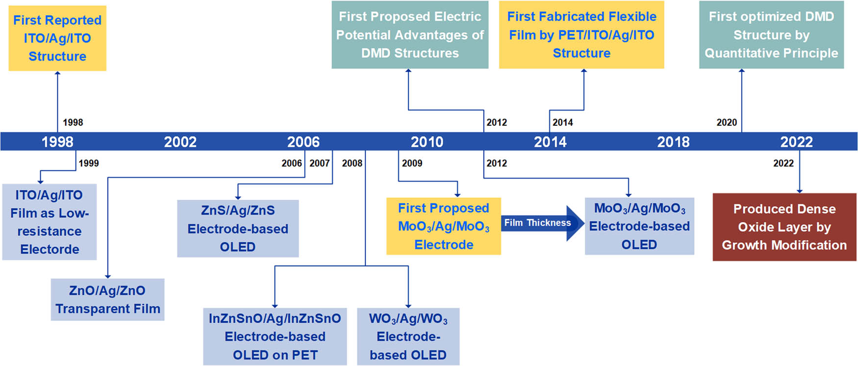
The roadmap of the DMD electrodes applied in LEDs.
Until now, the rapid development of optoelectronic devices has prompted a variety of DMD electrode configurations. High-performance DMD electrodes have always been in the spotlight both in science and industry [37,38,39,40,41]. In particular, the growth of ultrathin films [41], the selection of materials and structures [40], and their application in the photovoltaic scene [37] have been reviewed elsewhere. Notably, in 2023, Guo et al. comprehensively discussed the optoelectronic properties of ultrathin metal films in terms of electrostatic rate scattering models and other aspects, and reviewed in detail the mechanical properties of brittle/ductile hybrid structures [42]. The outstanding work provided guidance for enhancing the intrinsic optoelectronic properties of ultrathin metal films used for transparent guide applications. However, the application of DMD electrodes in LEDs has been rarely concluded, notably in the still-emerging field of foldable LEDs. It is crucial to stress that foldable devices are unique explorations and have exceptional effects in LED applications, such as touch displays. The review highlights the latest progress and identifies key challenges of DMD electrode design and their application in foldable light-emitting devices. Due to the small amount of DMD foldable devices, we also review DMD flexible devices due to the inclusion relationship between “flexible” and “foldable.” We begin by briefly introducing the optical and electrical properties of multilayer DMD structure films. According to Haacke’s
2 Multilayer DMD structure films’ optical and electrical properties
The outstanding optical transmission and electrical conduction are two noteworthy benefits of multilayer DMD structure films. The unique electrical property of DMD films is governed by the thin metal layer sandwiched between the top and bottom dielectric components. Metals are good conductors, and the electron transport greatly influences the resistivity of DMD films [41]. The resistance of the thick metal is summarized in Table 1. The sheet resistance of the monolayer metal film is further reduced by increasing the film thickness to mitigate the parasitic electrical loss. However, the transmittance of metal films decreases with the increase in the thickness by changing the film’s reflection and absorption of light.
Resistivity (ρ), complex refractive index (
| Material | Resistivity, ρ (Ω m) @ 20℃ | Complex refractive index, n − ik @ 550nm | Work function (ø/eV) | E adh (mJ/m2) | γ m (mJ/m2) |
|---|---|---|---|---|---|
| Silver (Ag) | 1.59 × 10⁻⁸ | 0.15 − i3.2 | 4.64 | 174 | 814–926 |
| Copper (Cu) | 1.70 × 10⁻⁸ | 0.68 − i2.6 | 5.10 | 474 | 1,233 |
| Gold (Au) | 2.44 × 10⁻⁸ | 0.42 − i2.3 | 5.47 | 227–246 | 1,125 |
| Aluminum (Al) | 2.82 × 10⁻⁸ | 0.97 − i6.4 | 4.20 | 844 | 844 |
| Nickel (Ni) | 6.99 × 10⁻⁸ | 1.9 − i3.6 | 5.22 | 803–942 | 1,883 |
| Iron (Fe) | 1.00 × 10⁻⁷ | 2.9 − i2.9 | 4.68 | 913 | 1,673 |
There is a very large refractive index mismatch between the metal electrode and the external environment (the air), that is, the impedance mismatch during electromagnetic wave transmission. This mismatch causes the electromagnetic wave to be reflected to a certain extent, thus reducing the transmittance. Based on Beer–Lambert law, light exhibits exponential attenuation with increasing film thickness and has a finite penetration depth in transparent electrodes [43]. The length at which the propagating light's intensity is diminished by more than 99% is referred to as the penetration depth [44]. Metal films with a thickness above the penetration depth have high reflectivity and opacity [45,46]. Therefore, the thickness of the metal in transparent electrodes is desired to be <10 nm [47,48]. The optical transmittance in thick metals is hindered by the metal's absorption of light. As light travels through metals, the widely distributed electronic states in metals combined with photons cause Joule heat and optical absorption loss. The absorbed photon energy is proportional to
The metal absorption loss occurs when the photon frequency is greater than the metal plasma frequency. In comparison, when the photon frequency is equal to the plasma frequency, the surface plasmon polaritons (SPPs) are resonantly excited by the coupling between the evanescent light traveling along the metal surface and incident light [55,56]. For the far field transmittance, the excitation of SPPs means the loss of the light out-coupling energy, as shown in Figure 3(a). The dispersion of SPPs can be calculated by conventional Maxwell’s equation as follows:
where
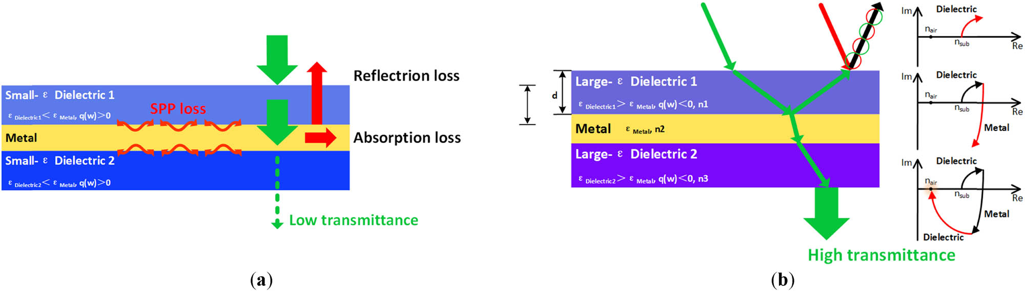
(a) Three types of optical losses in multilayer DMD structure films; (b) optimized DMD structures maximize optical transmittance.
Moreover, when photons with frequencies lower than the metal plasma frequency are encountered, metal films exhibit strong reflection due to the high electron density. The surface of translucent metal partially reflects the incident light, which causes significant reflection loss as seen in Figure 3(a). Considering the film thickness of Dielectric1, the optical path difference of reflected light is
The refracted light of the DMD film causes destructive interference as plotted in Figure 3(b) [44]. In this case, the reflection loss of the metal surface is forbidden. The DMD structure with the ultrathin metal layer coated by high-refractive index dielectric films has admittance diagrams as sketched in Figure 3(b). When the conductivity path from the substrate to the air is uninterrupted, according to the admittance diagram, there is a zero-reflection condition. Hence, we can detect the anti-reflective effect in the visible region by placing the last dielectric layer on the metal film to complete the conduction channel. The admittance of the DMD film starts from the substrate (n sub, 0) and ends near the air (n air, 0) to obtain zero-reflection conditions [55].
One of the key challenges in obtaining high conductivity is fabricating ultrathin metal films. As far as nanoscale metals are concerned, high transmittance and conductivity are associated with the surface morphology of metal films. During the metal preparation progress, the lattice mismatch between metals and substrates gives rise to aggregated island metal clusters before a homogeneous layer [61]. Sytchkova et al. [62] and Guske et al. [63] both reported that the thickness of metal films should be >10 nm to be continuous. Because the thickness of metal interlayers in DMD structures should be less than 10 nm, the surface roughness of metals is of decisive importance. The ultrathin metal layer with a rough surface inspires strong SPPs, which represents a further optical loss [56]. Meanwhile, the boundary effect in ultrathin films enhances obvious electron scattering at grain boundaries and surfaces, which causes highly reduced electron mobility and suppressed conductivity [64]. Nonetheless, it has been reported that the thickness of the continuous metal film can be < 10 nm by lowering the permeation threshold of the metal film [65]. Once reaching the percolation threshold, the separate metal island boundaries merge and form a continuous closed layer [45]. Dramatic reduction in surface roughness of the continuous closed layer steeply improves ultrathin metal film conductivity and reduces scattering and SPPs. Therefore, the film thickness can be optimized by minimizing the permeation threshold of the metal. The permeation threshold is reduced by adjusting mismatched surface energy between metal and dielectrics [66]. With a minimum permeation threshold, optical transmission improvement and electrical resistance reduction targets of the ultrathin metal film can be realized simultaneously [47].
It is noteworthy that DMD electrodes based on viable dielectric materials can be used as anodes and cathodes in light-emitting devices. A bandgap of above 3.1 eV (allowing >80% transmittance in the visible region), and carrier density of about 1020–1021 cm−3 are required of dielectrics used in FTCEs [67]. Moreover, the charge injection characteristic is the priority concern for dielectric components between metals and organics. The energy barrier for the charges to transfer hardly is formed between metals and organics, caused by the mismatched work function and molecular orbital (HOMO or LUMO) energy level. In devices using DMD anodes (cathodes), the approach to reduce the barrier height for charge injection increases (decreases) the work function of the dielectric between metals and organics in DMD anode (cathode), toward the ultimate goal of achieving Ohmic contacts. WO3 (4.8 eV) [68] and MoO3 (6.6 eV) [69] have been reported in optoelectronic devices. However, the dielectric between metal and substrate first focuses on high refractive index and surface energy instead of an injection of charge. High refractive index dielectrics coated on metals give the antireflective effect, and high surface energy dielectrics improve the uniformity of metal-deposited films. ZnS (surface energy of about 76 dynes/cm and refractive index n ZnS = ∼2.3) [70], WO3 (surface energy of about 69 dynes/cm and refractive index n WO3 = ∼1.95) [71,72], and MoO3 (surface energy of about 74 dynes/cm and refractive index of n MoO3 = ∼2.1) [73,74] have been reported as high surface energy dielectrics.
Table 2 lists various multilayer DMD structure films and their optical and electrical properties. As we can see, sheet resistances of reported the multilayer DMD structure films are generally below 20 Ω/□. Some multilayer DMD structure films have a sheet resistance of fewer than 10 Ω/□, which meets the requirements of large-area device electrodes. In addition, it is by the law of film transmittance that the transmittance of multilayer DMD structure film decreases with the increase in the metal thickness. The values of
Comparison of parameters of various DMD structures
| Substrate | Multilayer structure | Thickness [75] | R sh (Ω/□) | λ [75] | T (%) | Haake
|
Ref. |
|---|---|---|---|---|---|---|---|
| Glass | ITO | — | 18.9 | 450–600 | 96 | 35.2 | [76] |
| PET | ITO/Au/ITO | 45/7/45 | — | 550 | — | 24 | [77] |
| PET | ITO/Au/ITO | 20/8/20 | 16.7 | 550 | 88 | 16 | [78] |
| PET | ITO/Ag/Au/ITO | 20/7/7/20 | 6.7 | 550 | 84 | 24 | [78] |
| Glass | ITO/Ag/ITO | 35/10/20 | 6 | 550 | 90 | ∼85 | [79] |
| PET | ITO/Cu/ITO | 35/6/35 | 11.8 | 550 | 73.9 | 4.12 | [80] |
| PET | ZnO/Ag/ZnO | 25/8/25 | 16.7 | 550 | 77 | 4 | [78] |
| PET | ZnO/Au/ZnO | 25/8/25 | 16.7 | 550 | 82 | 8 | [78] |
| PET | ZnO/Ag/Au/ZnO | 25/8/9/25 | 10 | 550 | 83 | 15 | [78] |
| Glass | ZnO/Ag/ZnO | 30/8/30 | 6.1 | 400–700 | — | 8.6 | [81] |
| Glass | ZnO/Ag/ZnO | 30/10/30 | 5.4 | 400–700 | — | 22.4 | [81] |
| Glass | AZO/Ag/AZO | 30/8/30 | 5.6 | 400–700 | — | 29.2 | [81] |
| Glass | AZO/Ag/AZO | 30/10/30 | 5.3 | 400–700 | — | 45.5 | [81] |
| PET | AZO/Au/AZO | 40/7/40 | — | 550 | — | 8 | [77] |
| Glass | ZnS/Ag/ZnS(annealing temperature@25℃) | 35/17/35 | 19 | 550 | 55.6 | 0.15 ± 0.02 | [82] |
| Glass | ZnS/Ag/ZnS(annealing temperature@100℃) | 35/17/35 | 12 | 550 | 65.1 | 1.14 ± 0.2 | [82] |
| Glass | ZnS/Ag/ZnS(annealing temperature@200℃) | 35/17/35 | 8 | 550 | 79.2 | 12 ± 2.7 | [82] |
| PET | WO3/Ag/WO3 (WAW) | 30/10/50 | 12.2 | 400–700 | 80.9 | 9.84* | [83] |
| PET | WAW | 25/11/25 | 20 | 400–750 | 82.5 | 7.3* | [84] |
| Glass | MoO3/Ag/MoO3 | 20/7.5/20 | 48.3 | 300–700 | 66.1 | — | [85] |
| Glass | MoO3/Ag/MoO3 | 20/10/20 | — | 300–700 | 68.9 | 3.1 | [85] |
| Glass | MoO3/Ag/MoO3 | 20/7.5/20 | 8 | 300–700 | 79 | 12 | [85] |
| PET | MoO3/Ag/MoO3 | 17.5/11/35 | 13 | 350–700 | 74 | 4.21 | [86] |
| PET | MoO3/Ag film/MoO3 | 40/10/40 | 6.12 | 550 | 69.8 | 4.47 | [87] |
| PET | MoO3/Ag grid/MoO3 | 40/10/40 | 5.88 | 550 | 76.5 | 11.6 | [87] |
| Glass | TiO2/Ag/TiO2 | 35/8.5/35 | 5.62 | 450–650 | 85 | 35 | [76] |
| Glass | TiO2/Ag/TiO2 | 35/10/35 | 4.33 | 450–650 | 85 | 40.4 | [76] |
| Glass | TiO2/Ag/TiO2 | 35/13/35 | 3.74 | 450–650 | 84 | 13.2 | [76] |
| Glass | TiO2/Ag/TiO2 | 42/8.5/42 | 5.95 | 450–650 | 85 | 33.1 | [76] |
| Glass | TiO2/Ag/TiO2 | 42/10/42 | 4.48 | 450–650 | 89 | 69.6 | [76] |
| Glass | TiO2/Ag/TiO2 | 42/13/42 | 3.50 | 450–650 | 82 | 39.3 | [76] |
| PET | TiO2/Au/TiO2 | 30/7/30 | — | 550 | — | 1 | [77] |
| PET | Bi2O3/Au/Bi2O3 | 120/7/120 | — | 550 | — | 0.5 | [77] |
* Calculated from available data R sh and T% from graphs.
Furthermore, new structures of multilayer metal-dielectric films are derived from the DMD structures. Figure 4 illustrates three structures, which are asymmetric multilayer DMD structure [33], multilayer dielectric/metal/dielectric/metal/dielectric (DMDMD) structure [6], and multilayer metal/dielectric/metal (MDM) structure [88]. Asymmetric multilayer DMD structure films, which are considered to be effective waveguides, exist in a plasmonic quasi-bandgap (PQB) region [89]. SPPs are forbidden in the PQB region. For instance, a blue OLED based on asymmetric DMD electrodes, which effectively suppressed SPPs loss in the wavelength region of 390–470 nm, was introduced by Lee et al. [90]. Besides, multilayer DMDMD structure films, which have another coat of dielectric/metal on DMD films, can obtain better conductivity without a metal thickness increase. Destructive interference by the interface reflective beam and constructive interference by the interlayer transmitted beam still control the optical transmission of multilayer DMDMD structure film [91,92]. Therefore, color conversion of light can be realized by adjusting the reflection and transmission coefficients in DMDMD films. A good example is that Choi et al. analyzed the feasibility of multilayer DMDMD structural films for color conversion electrodes, and produced multilayer WAW electrodes applied in red and green ultra-high resolution OLED displays [93]. Following is the multilayer MDM structure, in which a significant change in the dispersion relation occurs due to four metal interfaces. MDM films are proposed to be filter electrodes in light-emitting, considering that Biring et al. obtained high color purity optoelectronic devices by using MDM electrodes in 2021 [88].
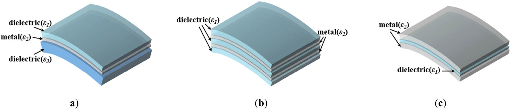
Three new multilayer metal-dielectric structures: (a) asymmetric multilayer DMD structure; (b) multilayer DMDMD structure; and (c) multilayer MDM structure.
3 Multilayer DMD structure films’ mechanical properties
A flexible object with a reduced bending radius is said to be foldable. The ability of an object to bend without rupturing atomic bonds is known as flexibility, and it is often measured by a threshold radius of curvature. A criterion for electrical failure in light-emitting devices is the threshold radius of curvature at which a transparent conducting electrode's resistance fails to revert to its initial value [94]. According to the various threshold radius of curvature, flexible displays can be classified into bendable (about 10 mm), rollable, and foldable (less than 5 mm) devices [95]. Obviously, devices with a larger threshold radius of curvature are simpler to implement, and foldable devices introduce new criteria for choosing an electrode.
Mechanical failure is still the key challenge for foldable devices due to the local channeling crack of the merged pre-existing flaws [96,97]. More specifically, pre-existing flaws propagation in films causes mechanical failure, and the fracture toughness is a key factor in providing uniform integrity and reliable performance throughout the foldable devices, which hinders the pre-existing cracks connection [98,99]. In traditional optoelectronic devices, fragile ITO electrodes are unable to withstand various deformations under bending, twisting, or folding [100]. In particular, the high fracture toughness of traditional ITO-based LEDs is difficult to achieve. According to the conventional Euler–Bernoulli beam theory, the reduced thickness of fragile ITO films facilitates the release of mechanical stress and strain [101]; however, this inevitably results in a loss of the electrical conductivity of ITO films. Multilayer ITO/metal/ITO structures have been proposed to avoid the performance degradation caused by the reduced material thickness [102]. Monolayer dielectric electrodes typically have a thickness between 150 and 700 nm [77], which is significantly thicker than the 20–50 nm dielectric layer used in multilayer DMD structure films [37]. Studies on mechanical properties and failure mechanisms have been reported. In 2015, Kim et al. showed that the flexibility of PET-based ZnSnO (ZTO)/Ag/ITO electrodes was far better than ITO thin films with the same thickness [103]. The sheet resistance of the multilayer electrode is almost unchanged after the bending cycle experiment due to the highly flexible metal film. In contrast, the value of ITO thin film sheet resistance noticeably rises. Consequently, DMD electrodes, which are significantly thinner than ITO electrodes, have higher fracture toughness and can, to a limited extent, preserve structural stability during bending and stretching.
Mostly due to the crack deflection, the DMD structure exhibits outstanding mechanical flexibility that is comparable to the layered structure of living organisms. The mixed brittle and ductile DMD structure is able to stop rapid crack propagation because the ductile metal layer specifically controls the slip and nonlinear deformation of the interface during bending. According to the penetration competition mechanism, the competition between the direction of the largest mechanical driving force and the direction of the path of the weakest structure will also cause the crack path to be diverted laterally along the metal layer when the DMD structure is bent [42].
The DMD structure provides unique mechanical flexibility mainly due to the excellent ductility of the metal layers. Hengst et al. proposed that the value of crack onset strain (COS) of the dielectric film decreases with the increase in the film thickness [104], as shown in Figure 5(a). Monolayer dielectric film was prone to catastrophic failure since the film was cracked by the formation and expansion of groove cracks perpendicular to the direction of the tensile load. In contrast, multilayer DMD film supported a more immense strain at the interface when cracking occurred and had better stability. To further analyze the fracture mechanics of multilayer DMD structure at the nanoscale level during bending, Lee and Guo confirmed the absorption of shear deformation by the flexible metal film [105]. As shown in Figure 5(b), cracks in multilayer films had a deflection effect, and the thin metal layer sandwiched between two layers of brittle material had a fracture toughness.
![Figure 5
(a) On 25 μm PET substrates, the COS of a-Si:H, ITO-1, ITO-2, and ZTO films were examined. Likewise, cross-sections of a-Si:H, ITO-1, and ITO-2 films after tensile loading perpendicular to the crack path up to a maximum strain value is indicated in (a), (b) and (c) [104]; (b) linear elastic crack-deflection mechanics solution of He and Hutchinson for a crack normally impinging an interface between two elastically dissimilar materials and comparison of flexible electrode cyclic performance results. (A) Curve marks the boundary between systems in which cracks are likely to penetrate the interface (above the curve, red square dot) (B) or deflect along the CuAg interface (below the curve, blue square dot). Also included are the optimization findings from a dynamic external bending fatigue test on a multilayer DMD material with a fixed external bending radius of 5 mm and longer bending periods. In comparison to AgNW and metal mesh (MM) samples (containing Ag nanoparticles), DMD materials displayed remarkably stable resistance values after more than 10,000 bending cycles [105].](/document/doi/10.1515/ntrev-2023-0578/asset/graphic/j_ntrev-2023-0578_fig_005.jpg)
(a) On 25 μm PET substrates, the COS of a-Si:H, ITO-1, ITO-2, and ZTO films were examined. Likewise, cross-sections of a-Si:H, ITO-1, and ITO-2 films after tensile loading perpendicular to the crack path up to a maximum strain value is indicated in (a), (b) and (c) [104]; (b) linear elastic crack-deflection mechanics solution of He and Hutchinson for a crack normally impinging an interface between two elastically dissimilar materials and comparison of flexible electrode cyclic performance results. (A) Curve marks the boundary between systems in which cracks are likely to penetrate the interface (above the curve, red square dot) (B) or deflect along the CuAg interface (below the curve, blue square dot). Also included are the optimization findings from a dynamic external bending fatigue test on a multilayer DMD material with a fixed external bending radius of 5 mm and longer bending periods. In comparison to AgNW and metal mesh (MM) samples (containing Ag nanoparticles), DMD materials displayed remarkably stable resistance values after more than 10,000 bending cycles [105].
In the ductile metal layer, metallic bound rupture helps with the absorption of impact energy and the prevention of rapid crack propagation. The impact energy is largely consumed in the elastic strain of the metal layer, which is used for the crack tip-blunting effects of plastic deformation. Lee proposed that the stress in front of the crack tip in ITO is almost 1 GPa, which is 40% higher than that of the DMD surface [106]. This means less energy is used for crack propagation and creating new surfaces in DMD structures. According to He and Hutchinson’s crack-deflection mechanics solution [107], the shear deformation of metal layers absorbs energy and transfers strain energy to plastic deformation, controlling the crack propagation along the metal/dielectric interlayer and forming a very unusual stepped two-dimensional crack as seen in Figure 6. Compared with penetrating cracks in brittle dielectric materials, deflection cracks are the more reliable mechanism to prevent rapid electrical failures. The penetrating crack represents the worst case of the destroyed films. The crack path of a stepped two-dimensional crack depends on two main factors. One is the Dundurs’ elastic mismatch parameter calculated as follows:
where
where
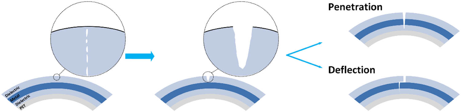
Development of cracks during bending of multilayer DMD films.
Nevertheless, the mechanical stability of DMD structures remains problematic. It is generally known that films placed on polycrystalline structures crystallize easily, therefore the dielectric deposited on polycrystalline metals forms crystallization of polycrystalline structures, degrading the mechanical properties of DMD films [108]. To address this issue, Song et al. added hydrogen to the oxide layer of ITO/Ag/ITO in 2021, resulting in the formation of a reliable amorphous oxide structure. The device's dynamic bending experiment demonstrates that by adding 0.2% hydrogen flow ratio, the mechanical stability of the material is greatly enhanced. Additionally, the residual stress is minimal and resistance changes are stable [109]. The majority of DMD film with unexpected polycrystalline structures can have their mechanical stability increased by adding the right amount of hydrogen during deposition, which further distinguishes DMD electrode from other developing transparent conductor alternatives.
Though the combination of the thin dielectric layer and the metal film gives the DMD electrodes outstanding mechanical flexibility, bending DMD electrodes undergo external bending tensile stress and internal bending compressive stress. Microcracks in multilayer films are inevitable after repeated bending due to the sizeable elastic strain differences between metal, brittle dielectric, and substrate materials [107,110]. Furthermore, the interfacial failure between DMD and substrate is another key challenge worth attention. Due to the large mechanism mismatch between the substrate and dielectric, cracks spread along the dielectric/substrate interface (i.e., delamination), causing interfacial failure [111,112]. Under the action of additional strain, new cracks are formed, and the spacing between cracks decreases gradually until reaching saturation. Under continuous strain, transverse cracking and stratification occurred. When the adhesion of the dielectric on the substrate is weak, stratification is easy to occur. Therefore, to produce foldable electrodes with high stability, a multilayer DMD structure with strong adhesion is necessary. The adhesion of the dielectric-substrate interlayer can be improved by pretreatment of the polymer surface with an ion beam or plasma before oxide deposition. The connection between the dielectric and the substrate is mainly composed of van der Waals forces. By pretreatment, chemical bonds can be formed at the interface between the DMD electrode and polymer surface. When the electrode–substrate film bend under intense stress, the new bonds may lead to additional interface.
Additionally, when bent inward or outward, DMD films on flexible substrates exhibit entirely different fracture mechanisms. The composite film experiences compression strain when it bends inward, which is first released by delamination and buckling. The DMD film may then be torn from the substrate and continue to conduct electricity before cracks occur, delaying device failure. The tensile strain applied to the composite film during outward bending is mostly discharged by the development of cracks, and the channel cracks directly form in the DMD film, resulting in quick device failure [42].
4 DMD on flexible substrates
The flexible substrate is the foundation of foldable and transparent devices. A flexible substrate requires excellent flexibility, great visible light transparency (up to 90%), a smooth surface, and thermal and chemical stability. So far, petroleum-derived substances with lightweight, thin thickness, high flexibility, and strong durability are the most common materials used for flexible substrates. PET [113], polyethylene naphthalene [114], and colorless polyimide [115,116] have been used in foldable devices, including OLEDs, QLEDs, and PeLEDs. Besides, various new flexible material substrates have been reported to meet the basic needs of flexible wearable devices, primarily in two categories: clothing-compatible fabric substrates [117,118,119,120,121,122,123] and biocompatible environmentally friendly substrates [124,125,126,127,128].
Despite the reports of a variety of flexible substrates, it is worth noting that previously reported traditional transparent electrodes, particularly DMD electrodes, combined with flexible transparent substrates typically have transmittance in visible wavelength that is lower than the transmittance of the monolayer substrate. However, as shown in Figure 7, in 2020, Ji et al. prepared DMD electrodes on PET substrates with an average absolute transmittance of 88.4% over the whole visible spectrum (400–700 nm), surpassing the transmittance of the substrate itself (88.1%) [35]. Quantitative design of the dielectric's composition and thickness, as well as the ultrathin, ultra-smooth copper-doped silver film, which surpasses the transmittance of transparent substrates, is how the device's relative transmittance of about 100.3% is achieved. This achievement opens up a remarkable new route for the replacement of traditional ITO devices. It is now possible to create electrode-substrate modules with extremely high transmittance owing to the solution to the problem of restricted transmittance in conventional electrode-substrate modules.
![Figure 7
Calculated (red solid curve) and measured (blue dashed curve) absolute transmittance from 400 to 700 nm of the designed DMD transparent electrode, showing great consistency with each other. The photograph of the fabricated flexible electrode shows high transparent and neutral appearance [35].](/document/doi/10.1515/ntrev-2023-0578/asset/graphic/j_ntrev-2023-0578_fig_007.jpg)
Calculated (red solid curve) and measured (blue dashed curve) absolute transmittance from 400 to 700 nm of the designed DMD transparent electrode, showing great consistency with each other. The photograph of the fabricated flexible electrode shows high transparent and neutral appearance [35].
Furthermore, a desired feature for flexible DMD-substrate films is low surface roughness to minimize the risk of shunts and leakage currents [129,130,131]. As seen in Table 3, the roughness of DMD-substrate films using polymer substrates such as PET is increased compared to those using conventional glass substrates. The use of a polymeric interlayer helps reduce the roughness of flexible DMD-PET film. For example, to modify the growth of TiOx/Ag/AZO electrodes on PET and make it resemble the growth of TiOx on glass, Kinner et al. employed a UV-crosslinked organic-inorganic composite (Amonil®) layer as the interlayer of PET and DMD electrodes [132].
Summary of the root mean square (RMS), and optical and electrical properties of the DMD structures deposited on different substrates
| Multilayer structure | Substrate material | RMS [75] | T 550 (%) | Rs (Ω/□) | Ref. |
|---|---|---|---|---|---|
| TiO x /Ag/AZO | Glass | 1.1 ± 0.1 | 90 | 5.7 | [132] |
| PET | 8.4 ± 1.5 | 47 | 29.9 | [132] | |
| PET/Amonil® 250 | 1.7 ± 0.1 | 87 | 5.7 | [132] | |
| PET/PMMA300 | 3.7 ± 2.3 | 81 | 6.9 | [132] | |
| ZTO/Ag/ZTO | Soda lime glass | 1.45 | 91.2 | 8.6 ± 0.2 | [133] |
| Polycarbonate | 3.00 | 77.2 | 6.7 ± 0.2 | [133] | |
| PET | 5.90 | 62.0 | 11.2 ± 0.2 | [133] | |
| SiO2/WO3/Ag/WO3 | Glass | — | 92 | — | [134] |
| Polyimide | 0.72 | 95 | — | [134] | |
| MoO3/Ag/MoO3 | Glass | 2.0 ± 0.2 | — | 5 | [135] |
| PET | 20.4 ± 1.5 | — | 5 | [135] |
5 Light-emitting devices using DMD electrodes
Flexible and transparent LEDs have drawn lots of interest because of their potential in portable and wearable electronic devices. Due to the limits of transparent electrodes, the electroluminescence (EL) performance of flexible light-emitting devices is thus still much worse than that of traditional displays. Meanwhile, flexible multilayer DMD electrodes have been utilized to create flexible light-emitting devices including OLEDs, QLEDs, and PeLEDs. Lewis et al. initially proposed flexible transparent OLED anodes made of ITO/Ag/ITO multilayer films in 2004 [136]. They demonstrated the outstanding robustness of the DMD-based OLEDs, which were anticipated to serve DMD films as transparent electrodes for OLEDs. In addition to the successful use of DMD electrodes in OLEDs, QLEDs and PeLEDs have a wide market and applied in the flexible electronics field. Benefiting from the quantum confinement effect, QLEDs offer superior color purity than OLEDs [137]. And the color purity of PeLEDs is also better than OLED [138]. However, compared to DMD-based OLEDs, the development of flexible QLEDs and PeLEDs with DMD electrodes is still in its infancy. Typical light-emitting device architectures with DMD top or bottom electrodes are shown in Figure 8, in which each layer’s material can be replaced by other functional materials with the same properties. In this review, OLEDs, QLEDs, and PeLEDs based on DMD electrodes are assessed from the views of physical properties, including turn-on voltage (V on), power efficiency (P.E.), current efficiency (C.E.), etc.
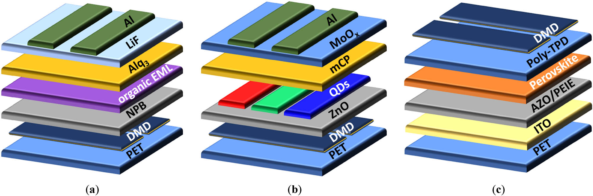
Typical architectures with DMD as top or bottom electrodes are given for (a) OLEDs; (b) QLEDs; and (c) PeLEDs.
5.1 Bottom- and top-emitting OLEDs using DMD electrodes
DMD electrodes are alternative technologies of transparent electrodes for next-generation OLEDs. At present, it is urgent to increase the efficiency, flexibility, and transparency of OLEDs using DMD electrodes. The traditional form of multilayer DMD structure is a single side electrode of efficient top/bottom OLEDs. The DMD electrode on the substrate is typically in the bottom-emitting OLEDs, and light is also released from the device's bottom surface that is in touch with the substrate. The output coupling challenge of light traveling through the DMD-substrate is the major issue for applying DMD to bottom-emission OLEDs.
Since the first demonstration of DMD structures, the photoelectric performance of DMD electrodes has been upgraded to the same level as ITO electrodes. The entire design of the device, including the functional layer injection barrier, microcavity effect, and the type of substrate, all have an impact on the luminous efficiency of bottom-emission DMD-OLEDs. For example, in 2010, Cho et al. systematically studied the optical properties of bottom DMD-OLEDs using a thin film optical framework with optical microcavity. The results suggested that the transmittance of the electrode could not guarantee high efficiency in DMD-OLEDs. The optical property of each layer of the DMD structure is different, and its optimization should consider not only the transmittance but also the overall cavity structure and its correlation with the emitter molecular emission spectrum. Extensive control can be exerted over the optical characteristics by precisely adjusting the relationship between the OLED’s microcavity effect and the DMD electrode's transmittance and their correlation with the emission spectrum of the emitting molecules. The luminous efficiency of DMD-OLED has increased to twice that of reference ITO-OLED with the alteration to the DMD structure, approaching Lambert emission [33]. This research examines optimization techniques for forward luminous efficiency, total optical power, and angle/spectral properties, which serve as the cornerstone for the effective application of DMD electrodes in OLEDs. In another experiment, the microcavity effect of the device depends on the thickness of the dielectric layer to adjust the optical path and round-trip phase. Yang et al. achieved high performance from ITO-free bottom OLEDs based on ZnS/Ag/ZnO/Ag/WO3 (ZAZAW) electrodes by careful tuning of dielectric layer thickness. In the visible light range, the electrode measured transmittance of over 80% with a very low resistance of 2.17 Ω/□. It was found that altering the microcavity effect by altering the thickness of WO3 will reduce the transmittance of ZAZAW electrode, but the efficiency of the PET-ZAZAW-based bottom-emitting OLEDs could be higher than that of PET-ITO-based OLEDs [91].
Additionally, higher performance bottom-emitting OLEDs require efficient charge injection at conditions that the transmittance of the DMD electrode is nearly equal to that of the ITO electrode. The electron injection capability of the device is based on the film resistance and injection barrier. A relatively smooth WAW conductive film has been proposed by thermal evaporation, which provides a good interface for electron injection. Meanwhile, BPhen:Cs2CO3 n-type doping layer was used to reduce the injection barrier of WAW/Bphen to 0.048 eV. The DMD-OLED has a maximum brightness of 280,000 cd/m2 at 8 V and an overall maximum current efficiency of 81.4 cd/A. The maximum external quantum efficiency (EQE) of bottom-emission OLED based on WAW cathode has reached 22.4%, which has reached the efficiency of ITO cathode devices [139]. However, the influence of substrate in the bottom-emitting OLEDs cannot be ignored. For instance, in 2021, Hermerschmidt et al. proposed TiO x /Ag/Al:ZnO transparent electrodes, and solution-treated OLEDs with these DMD electrodes have higher current efficiency and maximum brightness than commercial ITO-OLEDs. Compared to the reference ITO-OLED, DMD-OLED provides a 30% improvement in current efficiency with the glass substrate and a 260% improvement in current efficiency on PET substrate [36]. This discovery opens up the prospect of producing foldable devices at high throughput using DMD electrodes, and the type of substrate has a significant impact on the present efficiency of DMD-OLED devices, indicating the need to further explore the efficiency of DMD-OLED devices based on other types of flexible substrates.
Top-emission geometry can be helpful for the production of DMD-OLED with excellent performance and flexibility as compared to bottom emission devices. Since the light from the top-emitting device does not pass through the substrate, efficiency loss brought on by the substrate's parasitic light absorption can be avoided [33]. In 2021, Yoo et al. presented the top-emission geometry of the flexible and high-performance ultraviolet (UV) OLEDs with DMD electrode. The device has the potential to be used in the sectors of medicine, health, and cosmetics [140]. Research on top-emitting DMD-OLEDs is growing because DMD structures are appropriate for non-destructive top electrodes, despite the fact that these OLEDs are less prevalent than bottom-emitting devices. The design of the electrode and the structure of the device have an impact on the performance of the top emission DMD-OLED, much like with the bottom emission devices. For example, the DMD electrode's metal film causes the EL spectrum to shift due to their metal reflectance, resulting in the color distortion of the light, even in the case of ultrathin metal films [141]. Initial efforts to tackle low efficiency optimized the metal and dielectric layers, respectively. For instance, the WAW electrode uses the high refractive index dielectric material WO3 as the refractive index matching layer to increase optical transmission by multiple reflections and interference. The optimal structure of WO3 (30 nm)/Ag (12 nm)/WO3 (30 nm) is obtained, with high transmittance of up to 93.5% and low resistance of about 7.22 Ω/□. Meanwhile, the Al interlayer with low function is introduced to lower the barrier to electron injection of WO3 into Alq3 and decreased the operating voltage of OLED at J = 10 mA/cm2 by 6.9 V. The maximum luminance value (J = 220 mA/cm2) was increased from 8,400 to 11,700 cd/m2, and the luminescence efficiency was improved by about 26% when WAW cathode was used to replace the top Al cathode [142]. Thus, it has been demonstrated that adjusted DMD electrodes can increase the light output and electron injection efficiency of top-emitting OLEDs. Through further tuning, the DMD electrode structure was transformed into a double-layer metal sandwich that offers high transmittance via optical phenomena in the proper region between the two metal films. The parallel connecting principle also contributes to the electrode's high conductivity. In WO3/Ag/WO3/Ag/WO3 electrodes with double-layer metal film structures, high electrical conductivity (∼3 Ω/□) and high transparency (∼90%) were observed, according to Han et al. [143]. The performance of top-emitting OLED with the WO3/Ag/WO3/Ag/WO3 electrode is comparable to that of the device using ITO as the anode.
Nevertheless, the impact of the high melting point dielectric material evaporation process on the functionality of the device, cannot be disregarded. In 2019, Huang et al. demonstrated the highly efficient top-emitting white OLEDs with WAW transparent top cathode, which have better performance than that of the normally used semi-transparent Mg:Ag cathode [144]. The maximum EQE of device reached 17.47%. However, the photoelectric conversion efficiency of top emission OLEDs based on DMD electrodes is lower than that of bottom emission devices, which could be limited by the preparation process of DMD electrodes' dielectric on organic materials. Specifically, the organic functional layer in top emission OLEDs will be damaged when deposited with WO3 film since it has a high melting point of 1,473℃ [142], resulting in the photoelectric conversion efficiency of top emission OLEDs based on DMD electrodes becoming lower than that of bottom emission devices. The development of dielectric materials with low melting points and high conductivities is required since it can be demonstrated that the fabrication procedure of high melting point dielectric materials in DMD electrode has a detrimental influence on the performance of top emission devices.
In conclusion, DMD electrode has been extensively applied in the development of bottom and top-emitting OLEDs. Electrode design and device structure have been used to enhance DMD-OLED performance. However, additional study is required in the areas of substrate optical absorption loss for bottom emission devices and high melting point dielectric preparation technologies for top emission OLEDs. Due to the ubiquitous use of DMD electrodes in OLEDs, the remainder of this chapter will concentrate on OLEDs with particular characteristics, such as foldability and transparency.
5.2 Transparent OLEDs (TOLEDs) using DMD electrodes
The transparent devices industry is now targeted as another novel application by the OLED industry, transparent OLEDs based on DMD electrodes are rarely reported compared with flexible DMD-OLEDs. As transparent electrodes are required and the device must be translucent while yet allowing for effective luminescence, TOLED manufacturing technology is more complicated than flexible OLEDs (FOLEDs), making it more difficult to achieve good performance and stability.
Transparent electrodes are the key challenge in making TOLEDs, which can be made with transparent conductive oxides. However, the underlying organic layer may be damaged by the sputtering deposition of ITO or regular TCO, and getting highly clear TCO with good conductivity often needs a high temperature annealing procedure, which is inappropriate for OLEDs. To fulfill this issue, Yoo et al. created extremely transparent TOLEDs based on the top cathode of CS2CO3/Ag coated with ZnS layer in 2011. An ideal top electrode with low sheet resistance and high transmittance is proposed by combining the CS2CO3 layer with thermal evaporation. TOLED with peak transmittance up to 80% and luminous transmittance up to 76.4% is achieved, and the turn-on voltage of the device is as low as 2.6 V [145]. The dielectric layers in DMD electrodes can be easily prepared by thermal deposition, which provides an effective strategy for achieving highly transparent TOLEDs. In addition, alkali metals, especially calcium (Ca), are theoretically promising candidates for electrode metals, but they are limited by their high activity properties and require transparent conductive oxides for protection. To address this issue, Yu et al. produced TOLEDs in 2020 by coating ZnO on atomic layers to safeguard the thin, delicate Ca layer, which maintains both low work function (3.31 eV) and surface stability for organic electronics. Highly transparent (visible light range close to 90%) OLEDs have external quantum efficiencies of 22.7, 19.3, and 17.9% of green, yellow, and blue emissions, respectively [146]. These devices offer good options for transparent conductive electrodes in OLEDs and serves as an example of the potential of alkaline earth metal electrodes in organic electronics. The extensibility of DMD electrodes to various OLED designs, such as using DMD electrodes as both the cathode and the anode of OLED, was not investigated in these studies, which only took into account a small number of device structures and materials.
In previous studies of top- and bottom-emitting OLEDs, multilayer DMD structure films can only be applied to the single-side electrodes of OLEDs. The metal film to both sides of the device can result in the micro-cavity effect, which leads to a decrease in the film’s light output efficiency and an increase in the angle dependence of the light output. In 2015, Choi et al. first reported FTOLEDs using both multilayer DMD structure films as anode and cathode [14]. Figure 9(a) shows that the electrodes are ZnS/Ag/MoO3 (anode) and ZnS/Cs2CO3/Ag/ZnS (cathode), respectively. The PET-based FTOLEDs have a transmittance of over 74.22%, and the emission profile complies with the Lambertian emission pattern. Under compression stress, TFOLED with multilayer electrodes remains flexible, and at various emission angles, the EL intensity spectrum and CIE coordination exhibit hardly any variation. It is justified to investigate TOLEDs utilizing different materials for DMD electrodes because the proposed TFOLED design is regarded as a promising candidate design for transparent and flexible displays.
![Figure 9
(a) Photographs, schematic, and performance of highly transparent and flexible OLEDs: [14]; (b) device structure of the flexible OLED: schematic of the OLED device structure and energy-level diagram, the photograph of a large-area flexible OLED (50 mm × 50 mm) working at high luminance (>5,000 cd/m2) [150]; (c) highly efficient, heat dissipating, stretchable OLEDs based on a MoO3/Au/MoO3 electrode with encapsulation [151].](/document/doi/10.1515/ntrev-2023-0578/asset/graphic/j_ntrev-2023-0578_fig_009.jpg)
(a) Photographs, schematic, and performance of highly transparent and flexible OLEDs: [14]; (b) device structure of the flexible OLED: schematic of the OLED device structure and energy-level diagram, the photograph of a large-area flexible OLED (50 mm × 50 mm) working at high luminance (>5,000 cd/m2) [150]; (c) highly efficient, heat dissipating, stretchable OLEDs based on a MoO3/Au/MoO3 electrode with encapsulation [151].
In Section 5.1, WAW has been reported as the top electrode for top-emitting OLEDs; however, WO3 suffers from a high melting point (1,473°C [142]), compared to MoO3, which has a lower melting point (795°C [Hong, 2011 #421] ) and can effectively prevent the possibility of diffusion of hot atomic interfaces into the organic layer below. In 2018, Yeh et al. proposed a highly efficient inverted transparent OLED with a vacuum-deposited MoO3(5 nm)/Ag(12 nm)/WO3(40 nm) electrode, which has an overall device transmittance of 80% in visible-light wavelengths. The MoO3(5 nm)/Ag(12 nm)/WO3(40 nm) electrode prepared by vacuum thermal deposition showed very smooth surface morphology with RMS of 0.339 nm, OLED which demonstrates the total C.E., P.E., and EQE of 67.7 cd/A, 62.1 lm/W, and 20.1%. The bottom and top emission ratios of TOLED are nearly equal, at 1:1.1 [147], this means that the device emits light uniformly from the top and bottom and allows a large amount of light to pass through. The better performance of the device is attributed to the transparent MAW electrodes that act as a capping layer to regulate the emitting direction and optical properties. This means that the electrodes help control the direction of light emission and the way light interacts with the device. These studies provide very promising solutions for transparent displays and lighting devices, and it is of interest to explore the application of transparent and efficient OLED devices.
Recently, blue transparent DMD-OLEDs with high stability and light transmission for sleep management applications [148] and a new method for fabricating textile-based transparent DMD-OLEDs [149] have been reported, confirming the feasibility of transparent DMD-OLEDs for applications in various fields such as lighting and wearable displays. In conclusion, DMD electrodes have been used in transparent OLEDs. Since OLEDs also need to have better foldability in special scenarios such as wearable displays, in Section 5.3, we have focused on foldable DMD-OLEDs.
5.3 FOLEDs using DMD electrodes
Moreover, with the high flexibility and transparency of DMD structure, foldable and transparent OLEDs (FTOLEDs) with DMD electrodes and plastic substrates have been reported. According to the reports, the following challenges are the critical ones encountered in DMD electrode application in FOLED. On the one hand, achieving uniform and steady device performance is difficult due to the compatibility of the dielectric layer in the DMD electrode with the flexible substrate. On the other hand, FOLED is susceptible to mechanical stress and bending, which with time may result in the decline in performance and dependability.
To overcome these difficulties, new manufacturing techniques that work with flexible substrates were developed to create high-performance FOLEDs. Wang et al. obtained flexible OLEDs with a high EQE by depositing multilayer Ta2O5/Au/MoO3 structure films on plastic substrates [150], as shown in Figure 9(b). The device achieves an EQE of 40% at an extremely high brightness of 10,000 cd/m2, laying the foundation for the mass production of high-performance OLEDs on flexible plastic substrates. Additionally, in 2021, Choi et al. analyzed the stress and heat dissipation mechanisms of twistable and stretchable OLEDs based on MoO3/Au/MoO3 electrodes for the first time [151], as shown in Figure 9(c) The FTOLED was fabricated on thin NOA63 substrates doped with nanoparticles, and the light-emitting layer was made with horizontal emitting dipole and encapsulated with NOA63 for waterproofing. Nanoparticles effectively enhanced the light out-coupling and heat dissipation and reduced the triplet-triplet annihilation. The device achieved a C.E. of about 82.4 cd/A and an EQE of approximately 22.3% with minimal efficiency roll-off. In addition, the device significantly reduced the micro-cavity effect. The reported device further confirms the potential of foldable devices based on DMD electrodes and facilitates further development of stretchable and wearable devices.
In 2021, Guo et al. fabricated an ultrathin FOLED with a thickness of ∼1 μm using ITO/Cu-Ag/ITO electrodes and a polyvinyl alcohol (PVA) substrate. In this device, the DMD electrodes help improve the efficiency of the OLED by suppressing waveguide mode formation, while the PVA substrate forms an ultrathin substrate for a foldable OLED that folds well even when bent along the razor blade [152]. This research offers a potential solution for creating cost-effective OLEDs for foldable displays.
5.4 QLEDs and PeLEDs using DMD electrodes
Apart from OLEDs, QLEDs and PeLEDs based on DMD electrodes have been developed. However, DMD electrode-based QLEDs and PeLEDs have not been fully investigated yet and the device optoelectronic performance still lags behind that of common ITO-based devices, including low efficiency and instability. Table 4 summarizes the DMD-based QLEDs and PeLEDs reported in recent years. Currently, research on QLEDs and PeLEDs using DMD electrodes is still limited, especially on flexible substrates. To date, the majority of studies are surrounded on devices deposited on glass substrates.
Previous works on OLEDs, QLEDs, and PeLEDs with DMD electrodes
| LEDs type | Type of structure DMD vs standard configuration single ITO | LEDs architecture | Best performances compared to standard architecture | Ref. | ||||
|---|---|---|---|---|---|---|---|---|
| V on (V) | P.E. (lm/W) | C.E. (cd/A) | Luminance (cd/m2) | EQEmax (%) | ||||
| Bottom-emitting OLED | MoO3/Au/MoO3 (anode) | Glass/MoO3/Au/MoO3/NPB/Alq3:2 wt%C545T/Alq3/LiF/Al | 5.5 | — | 11.46 | — | — | [156] |
| MoO3/Au/MoO3 (anode) | Glass/MoO3/Au/MoO3/self-assembled monolayers/NPB/Alq3:2 wt%C545T/Alq3/LiF/Al | 4.5 | — | — | — | — | [157] | |
| ITO (anode) | Glass/ITO/2TNATA/NPB/Alq3:2 wt%C545T/Alq3/LiF/Al | 5.8 | — | — | — | — | [157] | |
| WAW (cathode) | Glass/WO3/Ag/WO3/BPhen:15 wt%CS2CO3/BPhen/CBP:8wt%Ir(ppy)3/TAPC/WO3/Ag | 3.2 | 66.7 | 81.4 | 1,000 | 22.4 | [139] | |
| ITO (cathode) | Glass/ITO/TAPC/CBP:8wt%Ir(ppy)3/BPhen/BPhen:15 wt%CS2CO3/Ag | — | 25 | 42.5 | 1,000 | 15.5 | [139] | |
| ZnO/Ag/ZnO (anode) | Glass/ZnO/Ag/ZnO/NPB/DMQA/BPhen/Al | 2 | — | — | — | +5 | [158] | |
| TiO2/Ag/MoO3 (anode) | Glass/TiO2/Ag/MoO3/TPD/Alq3/Al | — | 2.94 | 5.6 | — | — | [159] | |
| ITO (anode) | Glass/ITO/TPD/Alq3/Al | — | 1.97 | 4.05 | — | — | [159] | |
| Top-emitting OLED | WAW (cathode) | Silicon/Al:Cu:TiN/P-doped HIL/fluorescent yellow-doped HTL/fluorescent blue EML/HBL/N-doped ETL/WO3/Ag/WO3/SiO/Al2O3 | 2.1 | — | 5.86 | 2,000 | — | [160] |
| Ca/Ag (cathode) | Silicon/Al:Cu:TiN/P-doped HIL/fluorescent yellow-doped HTL/fluorescent blue EML/HBL/N-doped ETL/Ca/Ag/SiO/Al2O3 | 2.1 | — | 8.33 | 2,000 | — | [160] | |
| Ca:WAW (cathode) | Sub/anode/common layer/B-EML/charge generated layer/G-EML/R-EML/ETL/Ca:WAW | — | — | 43.23 | 4,323 | 17.47 | [144] | |
| Mg:Ag-CPL (cathode) | Sub/anode/common layer/B-EML/charge generated layer/G-EML/R-EML/ETL/Mg:Ag-CPL | — | — | 34.96 | 3,496 | 13.5 | [144] | |
| TOLED | MoO3/Ag/WO3 (anode) | Glass/ITO/BPhen:15 wt%Cs2CO3/BPhen/CBP:8wt%Ir(ppy)3/TAPC/MoO3/Ag/WO3 | — | 62.1 total | 68.7 total | — | 20.1 total | [147] |
| MoO3/Ag (anode) | ITO/BPhen:15 wt%Cs2CO3/BPhen/CBP:8wt%Ir(ppy)3/TAPC/MoO3/Ag | — | 65.6 | 83.5 | — | 22.7 | [147] | |
| ZnS/Ag/MoO3 (anode) and ZnS/Cs2CO3/Ag/ZnS (cathode) | PET/ZnS/Ag/MoO3/NPB/Alq3/ZnS/Cs2CO3/Ag/ZnS | 2.5 | 2.25 | — | — | — | [14] | |
| FOLED | MoO3/Au/MoO3 (anode) | NOA63+SiO2NPs/MoO3/Au/MoO3/NPB/TCTA/CBP:Ir(ppy)2tmd/TPBi/LiF/Al (the device luminance maintains stability up to 100 cycles with a strain of 30%) | — | 57.5 | 82.4 | — | 22.3 | [151] |
| MoO3/Ca:Ag/MoO3 (anode) | PET/UV resin/nanostructured MoO3/Ca:Ag/MoO3/TAPC/N,N‐dicarbazolyl‐3,5‐benzene (mCP):8 wt%FIrpic/mCP:6 wt%PO-01/TmPyPB/LiF/Al | — | 51.7 | 73.4 | 1,000 | 26.8 | [161] | |
| Nanostructured MoO3/Ca:Ag/MoO3 (anode) | PET/UV resin/nanostructured MoO3/Ca:Ag/MoO3/TAPC/mCP:8 wt%FIrpic/mCP:6 wt%PO-01/TmPyPB/LiF/Al (the device luminance maintains stability up to 800 cycles with bending) | — | 95.1 | 122.3 | 1,000 | 47.2 | [161] | |
| ZnO/Ag/ZnO:Ni (anode) | PET/ZnO/Ag/ZnO:Ni/MoO3/mCP/bis[4‐(9,9‐dimethyl‐9,10‐dihydroacridine)phenyl]sulfone (DMAC-DPS)/bis(2‐(diphenyl-phosphino)phenyl)ether oxide (DPEPO)/LiF/Al (the device performance maintains stability up to 2,000 cycles with bending radius of 6 cm) | 3 | 12 | 17.2 | 1157.3 | — | [162] | |
| ZnO/Ag/ZnO (anode) | PET/ZnO/Ag/ZnO/MoO3/mCP/DMAC-DPS/DPEPO/LiF/Al | 3.8 | 5.8 | 11.7 | 685.2 | — | [162] | |
| ITO (anode) | PET/ITO/Ni/MoO3/mCP/DMAC-DPS/DPEPO/LiF/Al | 3.3 | 10 | 16.1 | 855.2 | — | [162] | |
| ZnO/Ag/ZnO (anode) | Silica nanoparticles-based antireflective (AR)/PET/ZnO/Ag/ZnO/ethoxylated polyethyleneimine (PEIE)/super yellow (PDY-132)/1,4,5,8,9,1 1-hexaazatriphenylenehexacarbonitrile (Lumtec)/Al (the device luminance maintains 80% up to 900 cycles with bending radius of 6 cm) | 2.8 | — | 12.3 | 9,400 | 5 | [163] | |
| ZnO/Ag/ZnO (anode) | PET/ZnO/Ag/ZnO/PEIE/PDY-132/Lumtec/Al | 2.7 | — | 9.6 | 8,150 | 4 | [163] | |
| ITO (anode) | PET/ITO/PEIE/PDY-132/Lumtec/Al | 2.6 | — | 9.2 | 8,300 | 3.8 | [163] | |
| ZnS/Ag/MoO3 (anode) | PET/ZnS/Ag/MoO3/NPB/Alq3/Liq/Al/hybrid nanostratified moisture barrier (the performance of device after 1,000 cycles with bending radius of 3 cm maintains stability in 30 days at 30℃) | 2.5 | — | — | 3,860 | — | [164] | |
| ZnO/Ag/CuSCN (anode) | PET/ZnO/Ag/CuSCN/super yellow (SY)/LiF/Al (the device performance maintains 90% up to 1,000 cycles with bending radium of 5 cm) | 2.3 | — | 23.4 | — | — | [165] | |
| ZnO/Ag/CuSCN (anode) | Glass/ZnO/Ag/CuSCN/SY/LiF/Al | 2.3 | — | 15.2 | — | — | [165] | |
| ITO/CuSCN (anode) | Glass/ITO/CuSCN/SY/LiF/Al | 2.3 | — | 16.3 | — | — | [165] | |
| ITO/PEDOT:PSS (anode) | Glass/ITO/PEDOT:PSS/SY/LiF/Al | 2.3 | — | 15.1 | — | — | [165] | |
| ITO/Ag/ZTO (anode) | PET/ITO/Ag/ZTO/TAPC/HAT-CN/TAPC/HAT-CN/TAPC/HAT-CN/TAPC/CBP:8 wt%Ir(ppy)3/B3PYMPM/LiF/Al | 4.18 | 25.15 | 33.45 | — | 10.24 | [166] | |
| ZTO/Ag/ITO (anode) | PET/ZTO/Ag/ITO/TAPC/HAT-CN/TAPC/HAT-CN/TAPC/HAT-CN/TAPC/CBP:8 wt%Ir(ppy)3/B3PYMPM/LiF/Al | 4.39 | 31.55 | 44.03 | — | 13.07 | [166] | |
| ITO | Glass/ITO/TAPC/HAT-CN/TAPC/HAT-CN/TAPC/HAT-CN/TAPC/CBP:8 wt%Ir(ppy)3/B3PYMPM/LiF/Al | 4.07 | 39.11 | 50.59 | — | 16.4 | [166] | |
| QLED | ITO/Ag/ITO | PET/ITO/Ag/ITO/ZnO/red QDs/mCP/MoO3/Al | 2.0 | — | 16.3 | 106,896 | — | [167] |
| ITO/Ag/ITO | PET/ITO/Ag/ITO/ZnO/green QDs/mCP/MoO3/Al | 2.4 | — | 86.5 | 336,000 | — | [167] | |
| ITO/Ag/ITO | PET/ITO/Ag/ITO/ZnO/blue QDs/mCP/MoO3/Al | 2.8 | — | 16.1 | 18,127 | — | [167] | |
| ITO/Ag/ITO | PET/ITO/Ag/ITO/ZnO/red CdSe/CdS/ZnS QDs/mCP/CBP/MoO3/Al | — | 24.8 | — | 54,795 | 14.1 | [168] | |
| ITO/Ag/ITO | Glass/ITO/Ag/ITO/composed PFSA, PEDOT:PSS and dimethyl sulfoxide/red QDs/Zn0.85Mg0.15O NPs/IZO (@100℃-annealing) | 1.9 | — | 15.1 | — | 11.6 | [169] | |
| ITO/Ag/ITO | Glass/ITO/Ag/ITO/composed PFSA, PEDOT:PSS and dimethyl sulfoxide/red QDs/Zn0.85Mg0.15O NPs/IZO (@150℃-annealing) (top emission) | 1.9 | — | 24.8 | — | 20.1 | [169] | |
| ITO/Ag/ITO | Glass/ITO/Ag/ITO/composed PFSA, PEDOT:PSS and dimethyl sulfoxide/red QDs/Zn0.85Mg0.15O NPs/IZO (@200℃-annealing) | 1.8 | — | 7.6 | — | 5.7 | [169] | |
| ITO/Ag/ITO | Glass/ITO/Ag/ITO/composed PFSA, PEDOT:PSS and dimethyl sulfoxide/red QDs/Zn0.85Mg0.15O NPs/IZO (@250℃-annealing) | 2.6 | — | 1.5 | — | 1.2 | [169] | |
| ITO/Ag/ITO | PET/ITO/Ag/ITO/ZnO/red CdSe/ZnCdSe/ZnS QDs/CBP/MoO x /Al | ∼2 | 14.1 | 17.9 | 117,700 | 13 | [153] | |
| ITO/Ag/ITO | PET/ITO/Ag/ITO/PEDOT:PSS/ZnO/red CdSe/ZnCdSe/ZnS QDs/CBP/MoO x /Al | ∼2 | 16.3 | 20.4 | 58,590 | 14.8 | [153] | |
| Yb:MoO3 (0.2:1)/Ag/MoO3 | Glass/ITO/Ag/ITO/composed PFSA, PEDOT:PSS and dimethyl sulfoxide/green QDs/Zn0.85Mg0.15O NPs/Yb:MoO3 (0.2:1)/Ag/MoO3 | 2.2 | — | 11.8 | 1,000 | 2.9 | [154] | |
| Yb:MoO3 (0.6:1)/Ag/MoO3 | Glass/ITO/Ag/ITO/PFSA-PEDOT:PSS-dimethyl sulfoxide/green QDs/Zn0.85Mg0.15O NPs/Yb:MoO3 (0.6:1)/Ag/MoO3 | 2.2 | — | 38.0 | 1,000 | 9.8 | [154] | |
| Yb:MoO3 (1:1)/Ag/MoO3 | Glass/ITO/Ag/ITO/PFSA-PEDOT:PSS-dimethyl sulfoxide/green QDs/Zn0.85Mg0.15O NPs/Yb:MoO3 (1:1)/Ag/MoO3 | 2.3 | — | 28.0 | 1,000 | 7.4 | [154] | |
| IZO | Glass/ITO/Ag/ITO/PFSA-PEDOT:PSS-dimethyl sulfoxide/green QDs/Zn0.85Mg0.15O NPs/IZO | 2.2 | — | 30.9 | 1,000 | 8.1 | [154] | |
| MoO x /Ag/MoO x | PET/SU-8/MoO x /Ag/MoO x /ZnO NP/red CdSe/ZnS QDs/TAPC/WO x /Ag | — | — | 30.3 | — | — | [170] | |
| WO x /Ag/WO x | PET/SU-8/WO x/Ag/WO x /ZnO NP/(CdSe/ZnS) QD/TAPC/WO x /Ag | — | — | 19.4 | — | — | [170] | |
| PeLED | MoO3/Al/ITO/Ag/ITO | ITO/AZO/PEIE/FAPbI3/poly-TPD/MoO3/Al/ITO/Ag/ITO | ∼1.4 | — | — | — | 5.7/1.2 | [155] |
There are challenges in using DMD electrodes in QLEDs. The dielectric layer in the DMD structure must be compatible with the quantum dot material since it will influence the stability and performance of the quantum dots utilized in QLED. More crucially, like OLED applications, the DMD electrode's dielectric layer can operate as a barrier to electron injection, lowering QLED’s overall efficiency. This must be avoided by utilizing high power function metals or by adjusting the dielectric layer's thickness and composition. DMD structures in QLEDs are mainly ITO/Ag/ITO and MoO3/Ag/MoO3. In particular, ITO/Ag/ITO electrode-based QLEDs are more extensively studied and perform better. For instance, a flexible QLED based on PET/ITO/Ag/ITO/PEDOT:PSS was fabricated by Wang et al. with a device efficiency of 20.4 cd/A and an EQE of 14.8% in 2022 [153], as shown in Figure 10(a). After 300 bend cycles, these flexible QLEDs' injection/transfer and charge complex properties, as well as those of the related charge transport layer and quantum dots, remain unaltered. In contrast, the EQE of MoO3/Ag/MoO3 electrodes based QLEDs are all less than 10%, considering that photoelectric properties of QLED are limited by the p-type characteristics and high work function of dielectric materials [154].
![Figure 10
(a) The structure, absorption, and PL spectra, and emission images of QLED [153]; (b) the structure, EL spectra, and near-infrared photo of PeLED [155].](/document/doi/10.1515/ntrev-2023-0578/asset/graphic/j_ntrev-2023-0578_fig_010.jpg)
Furthermore, the research of PeLEDs based on multilayer DMD electrodes is just beginning. In the process of creating high-performance PeLEDs using DMD electrodes, researchers have made some progress. In 2020, Xie et al. announced a large-area (120 mm2) transparent near-infrared PeLED based on MoO3/Al/ITO/Ag/ITO electrodes with an EQE of just 1.2% emitted from the DMDMD electrode side [155], as illustrated in Figure 10(b). These findings support the DMD structure as a promising electrode for transparent and foldable devices. However, more research still has to be done on the optimization of device architecture, choosing appropriate materials, and alternative production techniques.
In conclusion, these efforts together enhance the efficacy, stability, and performance of LEDs utilizing DMD electrodes, which advances the creation of flexible, wearable lighting, as well as novel applications in other fields including automotive lighting and signs.
6 Summary and outlook
Multilayer DMD electrodes are promising for ITO-free foldable optoelectrical devices based on their excellent performance. An overview of the challenges of DMD electrodes, particularly in the physical properties, mechanism stability, and application reliability is mentioned. However, there are still challenges to address, particularly in the optical property, mechanism stability, and application reliability.
Concerning the optical property of DMD-based light emitting devices, since the full transparency of metal interlayer in the DMD electrode is hard to achieve, the metal reflected light which is not entirely eliminated causes the microcavity effect. Spectral narrowing and high spectral density in the vertical direction of the film plane, caused by the microcavity effect, limit the high optical transmittance in the wide optical wavelengths. The light out-coupling of DMD film is also affected by the angle of the incident light. The high angle dependence limits the viewing angle of transmitted light. Therefore, to reduce the microcavity effect and angle dependence, it is necessary to further minimize the reflected light from the metal layer, in other words, to reduce the thickness of metal layers. Metal nanowires/networks and alloy films combining highly conductive metal materials with low surface energy materials (e.g., Ag–Cu alloy films) are proposed to replace the single metal film layer in the DMD electrodes.
DMD electrodes exhibit the potential for bending strain, but the process of existing research has been slow. The mechanical flexibility of DMD electrodes is mainly limited by brittle films and interfacial failures. Since the metal layer is the decisive factor for the mechanical stability, it is hoped that future researchers will shift their focus to achieve better flexibility of the metal layer. This can be achieved by measuring the flexibility of various doped metal films. It might also be helpful to study DMD-derived structures with more metal layers such as MDMDM. Moreover, current congestion and subsequent short-circuiting occur at hot spots in the metal film of high-brightness LEDs during bending. Negative hot spots may be reduced by controlling the deposition conditions to obtain highly smooth, ultrathin metal films.
Further work is also needed on the reliability of metal films in DMD electrodes. Ag, which is currently widely used in DMD electrodes, is known to be a metal that is susceptible to oxidation easily. The reliability of Ag and other metals in DMD electrodes, exposed to environmental stressors such as chemical corrosion and mechanical strain, is still not fully explained. More research could focus on obtaining lower metal reducibility, such as doping Ag with a low-reducing Au. The negative environmental effects on metals can be reduced by flexible packaging with high water and oxygen resistance. It is hoped that researchers will shift their focus more to flexible packaging materials with better sealing properties.
With the further development of a new generation of foldable displays like OLEDs, QLEDs, and PeLEDs, the demand for foldable and transparent electrodes is increasing. The multilayer DMD structure film is the most ideal electrode for foldable and transparent displays due to its high optical transmittance, low film resistance, and high flexibility. At the same time, the sputtering process for its preparation can meet the needs of both high compatibilities with flexible substrates and large-scale preparation requirements. To date, research have been conducted on DMD electrodes from various aspects, such as theoretical methods, structural design, and device applications. In this review, we present the research progress in DMD electrodes. The excellent photoelectric and mechanical properties of DMD electrodes are systematically reviewed in this work. Moreover, the application in OLEDs, QLEDs, and PeLEDs based on flexible substrates are discussed and summarized. Although DMD electrodes have many advantages, there is still room for continuous improvement of its performance. DMD-based devices will surely be a new generation of flexible transparent displays that are applied to curved displays, electronic newspapers, wearable displays, and concept lighting panels.
-
Funding information: This work was supported by The Research Project of Beijing Municipal Natural Science Foundation (No. BJXZ2021-012-00046).
-
Author contributions: L.Z. had the idea for the article, B.Z. performed the literature search and data analysis, R.G. drafted, and Y.Z. critically revised the work. All authors have accepted responsibility for the entire content of this manuscript and approved its submission.
-
Conflict of interest: The authors state no conflict of interest.
-
Data availability statement: Data sharing is not applicable to this article as no datasets were generated or analysed during the current study.
References
[1] Kamiya T, Hosono H. Material characteristics and applications of transparent amorphous oxide semiconductors. NPG Asia Mater. 2010;2(1):15–22.10.1038/asiamat.2010.5Search in Google Scholar
[2] Yu X, Marks TJ, Facchetti A. Metal oxides for optoelectronic applications. Nat Mater. 2016;15(4):383–96.10.1038/nmat4599Search in Google Scholar PubMed
[3] Osada T, Kugler T, Bröms P, Salaneck W. Polymer-based light-emitting devices: investigations on the role of the indium-tin oxide (ITO) electrode. Synth Met. 1998;96(1):77–80.10.1016/S0379-6779(98)00069-1Search in Google Scholar
[4] Paine DC, Whitson T, Janiac D, Beresford R, Yang CO, Lewis B. A study of low temperature crystallization of amorphous thin film indium–tin–oxide. J Appl Phys. 1999;85(12):8445–50.10.1063/1.370695Search in Google Scholar
[5] Yahya M, Fadavieslam M. The effects of argon plasma treatment on ITO properties and the performance of OLED devices. Opt Mater. 2021;120:111400.10.1016/j.optmat.2021.111400Search in Google Scholar
[6] Lee S-M, Choi CS, Choi KC, Lee H-C. Low resistive transparent and flexible ZnO/Ag/ZnO/Ag/WO3 electrode for organic light-emitting diodes. Org Electron. 2012;13(9):1654–9.10.1016/j.orgel.2012.05.014Search in Google Scholar
[7] Oh SJ, Kwon JH, Lee S, Choi KC, Kim T-S. Unveiling the annealing-dependent mechanical properties of freestanding indium tin oxide thin films. ACS Appl Mater Interfaces. 2021;13(14):16650–9.10.1021/acsami.0c23112Search in Google Scholar PubMed
[8] Lee SM, Cho Y, Kim DY, Chae JS, Choi KC. Enhanced light extraction from mechanically flexible, nanostructured organic light‐emitting diodes with plasmonic nanomesh electrodes. Adv Opt Mater. 2015;3(9):1240–7.10.1002/adom.201500103Search in Google Scholar
[9] Van De Lagemaat J, Barnes TM, Rumbles G, Shaheen SE, Coutts TJ, Weeks C, et al. Organic solar cells with carbon nanotubes replacing In2O3: Sn as the transparent electrode. Appl Phys Lett. 2006;88(23):233503.10.1063/1.2210081Search in Google Scholar
[10] Han T-H, Lee Y, Choi M-R, Woo S-H, Bae S-H, Hong BH, et al. Extremely efficient flexible organic light-emitting diodes with modified graphene anode. Nat Photonics. 2012;6(2):105.10.1038/nphoton.2011.318Search in Google Scholar
[11] Fraser D, Cook H. Highly Conductive, Transparent Films of Sputtered In2−xSnxO3−y. J Electrochem Soc. 1972;119(10):1368.10.1149/1.2403999Search in Google Scholar
[12] Heo JH, Shin DH, Lee ML, Kang MG, Im SH. Efficient organic–inorganic hybrid flexible perovskite solar cells prepared by lamination of polytriarylamine/CH3NH3PbI3/anodized Ti metal substrate and graphene/PDMS transparent electrode substrate. ACS Appl Mater Interfaces. 2018;10(37):31413–21.10.1021/acsami.8b11411Search in Google Scholar PubMed
[13] Ma C, Liu Y-F, Bi Y-G, Zhang X-L, Yin D, Feng J, et al. Recent progress in post treatment of silver nanowire electrodes for optoelectronic device applications. Nanoscale. 2021;13(29):12423–37.10.1039/D1NR02917GSearch in Google Scholar PubMed
[14] Kim DY, Han YC, Kim HC, Jeong EG, Choi KC. Highly transparent and flexible organic light‐emitting diodes with structure optimized for anode/cathode multilayer electrodes. Adv Funct Mater. 2015;25(46):7145–53.10.1002/adfm.201502542Search in Google Scholar
[15] Haacke G. New figure of merit for transparent conductors. J Appl Phys. 1976;47(9):4086–9.10.1063/1.323240Search in Google Scholar
[16] Yang L, Xiong Q, Li Y, Gao P, Xu B, Lin H, et al. Artemisinin-passivated mixed-cation perovskite films for durable flexible perovskite solar cells with over 21% efficiency. J Mater Chem A. 2021;9(3):1574–82.10.1039/D0TA10717DSearch in Google Scholar
[17] Hu X, Huang Z, Li F, Su M, Huang Z, Zhao Z, et al. Nacre-inspired crystallization and elastic “brick-and-mortar” structure for a wearable perovskite solar module. Energy Environ Sci. 2019;12(3):979–87.10.1039/C8EE01799ASearch in Google Scholar
[18] Bae S, Kim H, Lee Y, Xu X, Park J-S, Zheng Y, et al. Roll-to-roll production of 30-inch graphene films for transparent electrodes. Nat Nanotechnol. 2010;5(8):574–8.10.1038/nnano.2010.132Search in Google Scholar PubMed
[19] Yang Y, Min F, Qiao Y, Li Z, Vogelbacher F, Liu Z, et al. Embossed transparent electrodes assembled by bubble templates for efficient flexible perovskite solar cells. Nano Energy. 2021;89:106384.10.1016/j.nanoen.2021.106384Search in Google Scholar
[20] Kaskela A, Nasibulin AG, Timmermans MY, Aitchison B, Papadimitratos A, Tian Y, et al. Aerosol-synthesized SWCNT networks with tunable conductivity and transparency by a dry transfer technique. Nano Lett. 2010;10(11):4349–55.10.1021/nl101680sSearch in Google Scholar PubMed
[21] Hu X, Meng X, Zhang L, Zhang Y, Cai Z, Huang Z, et al. A mechanically robust conducting polymer network electrode for efficient flexible perovskite solar cells. Joule. 2019;3(9):2205–18.10.1016/j.joule.2019.06.011Search in Google Scholar
[22] HwanáKo S. A dual-scale metal nanowire network transparent conductor for highly efficient and flexible organic light emitting diodes. Nanoscale. 2017;9(5):1978–85.10.1039/C6NR09902ESearch in Google Scholar PubMed
[23] Lian L, Xi X, Dong D, He G. Highly conductive silver nanowire transparent electrode by selective welding for organic light emitting diode. Org Electron. 2018;60:9–15.10.1016/j.orgel.2018.05.028Search in Google Scholar
[24] Ok K-H, Kim J, Park S-R, Kim Y, Lee C-J, Hong S-J, et al. Ultra-thin and smooth transparent electrode for flexible and leakage-free organic light-emitting diodes. Sci Rep. 2015;5(1):1–8.10.1038/srep09464Search in Google Scholar PubMed PubMed Central
[25] Jiang S, Hou P-X, Chen M-L, Wang B-W, Sun D-M, Tang D-M, et al. Ultrahigh-performance transparent conductive films of carbon-welded isolated single-wall carbon nanotubes. Sci Adv. 2018;4(5):eaap9264.10.1126/sciadv.aap9264Search in Google Scholar PubMed PubMed Central
[26] Fan JC, Bachner FJ. Transparent heat mirrors for solar-energy applications. Appl Opt. 1976;15(4):1012–7.10.1364/AO.15.001012Search in Google Scholar PubMed
[27] Choi K, Kim J, Lee Y, Kim H. ITO/Ag/ITO multilayer films for the application of a very low resistance transparent electrode. Thin Solid Films. 1999;341(1–2):152–5.10.1016/S0040-6090(98)01556-9Search in Google Scholar
[28] Sahu D, Lin S-Y, Huang J-L. ZnO/Ag/ZnO multilayer films for the application of a very low resistance transparent electrode. Appl Surf Sci. 2006;252(20):7509–14.10.1016/j.apsusc.2005.09.021Search in Google Scholar
[29] Pang H, Yuan Y, Zhou Y, Lian J, Cao L, Zhang J, et al. ZnS/Ag/ZnS coating as transparent anode for organic light emitting diodes. J Lumin. 2007;122:587–9.10.1016/j.jlumin.2006.01.232Search in Google Scholar
[30] Tao C, Xie G, Liu C, Zhang X, Dong W, Meng F, et al. Semitransparent inverted polymer solar cells with MoO3/Ag/MoO3 as transparent electrode. Appl Phys Lett. 2009;95(5):206.10.1063/1.3196763Search in Google Scholar
[31] Ryu SY, Noh JH, Hwang BH, Kim CS, Jo SJ, Kim JT, et al. Transparent organic light-emitting diodes consisting of a metal oxide multilayer cathode. Appl Phys Lett. 2008;92(2):15.10.1063/1.2835044Search in Google Scholar
[32] Choi K-H, Nam H-J, Jeong J-A, Cho S-W, Kim H-K, Kang J-W, et al. Highly flexible and transparent InZnSnOx∕Ag∕InZnSnOx multilayer electrode for flexible organic light emitting diodes. Appl Phys Lett. 2008;92(22):194.10.1063/1.2937845Search in Google Scholar
[33] Cho H, Yun C, Yoo S. Multilayer transparent electrode for organic light-emitting diodes: tuning its optical characteristics. Opt Express. 2010;18(4):3404–14.10.1364/OE.18.003404Search in Google Scholar PubMed
[34] Tian B, Williams G, Ban D, Aziz H. Transparent organic light-emitting devices using a MoO3/Ag/MoO3 cathode. J Appl Phys. 2011;110(10):104507.10.1063/1.3662194Search in Google Scholar
[35] Ji C, Liu D, Zhang C, Jay Guo L. Ultrathin-metal-film-based transparent electrodes with relative transmittance surpassing 100%. Nat Commun. 2020;11(1):1–8.10.1038/s41467-020-17107-6Search in Google Scholar PubMed PubMed Central
[36] Kinner L, Dimopoulos T, Ligorio G, List-Kratochvil EJ, Hermerschmidt F. High performance organic light-emitting diodes employing ITO-free and flexible TiOx/Ag/Al:ZnO electrodes. RSC Adv. 2021;11(28):17324–31.10.1039/D1RA02214HSearch in Google Scholar PubMed PubMed Central
[37] Girtan M, Negulescu B. A review on oxide/metal/oxide thin films on flexible substrates as electrodes for organic and perovskite solar cells. Opt Mater: X. 2022;13:100122.10.1016/j.omx.2021.100122Search in Google Scholar
[38] Lee HB, Jin W-Y, Ovhal MM, Kumar N, Kang J-W. Flexible transparent conducting electrodes based on metal meshes for organic optoelectronic device applications: a review. J Mater Chem C. 2019;7(5):1087–110.10.1039/C8TC04423FSearch in Google Scholar
[39] Berny S, Blouin N, Distler A, Egelhaaf HJ, Krompiec M, Lohr A, et al. Solar trees: first large‐scale demonstration of fully solution coated, semitransparent, flexible organic photovoltaic modules. Adv Sci. 2016;3(5):1500342.10.1002/advs.201500342Search in Google Scholar PubMed PubMed Central
[40] Guillen C, Herrero J. TCO/metal/TCO structures for energy and flexible electronics. Thin Solid Films. 2011;520(1):1–17.10.1016/j.tsf.2011.06.091Search in Google Scholar
[41] Yun J. Ultrathin metal films for transparent electrodes of flexible optoelectronic devices. Adv Funct Mater. 2017;27(18):1606641.10.1002/adfm.201606641Search in Google Scholar
[42] Park Y-B, Lee S, Tobah M, Ma T, Guo LJ. Optimized optical/electrical/mechanical properties of ultrathin metal films for flexible transparent conductor applications: review. Opt Mater Express. 2023;13(2):304–47.10.1364/OME.473277Search in Google Scholar
[43] Abitan H, Bohr H, Buchhave P. Correction to the Beer-Lambert-Bouguer law for optical absorption. Appl Opt. 2008;47(29):5354–7.10.1364/AO.47.005354Search in Google Scholar
[44] Schubert S Transparent top electrodes for organic solar cells: Saechsische Landesbibliothek-Staats-und Universitaetsbibliothek Dresden; 2015.Search in Google Scholar
[45] Nehm F, Schubert S, Müller-Meskamp L, Leo K. Observation of feature ripening inversion effect at the percolation threshold for the growth of thin silver films. Thin Solid Films. 2014;556:381–4.10.1016/j.tsf.2014.01.067Search in Google Scholar
[46] Dionne J, Sweatlock L, Atwater H, Polman A. Planar metal plasmon waveguides: frequency-dependent dispersion, propagation, localization, and loss beyond the free electron model. Phys Rev B. 2005;72(7):075405.10.1103/PhysRevB.72.075405Search in Google Scholar
[47] Schubert S, Hermenau M, Meiss J, Müller‐Meskamp L, Leo K. Oxide sandwiched metal thin‐film electrodes for long‐term stable organic solar cells. Adv Funct Mater. 2012;22(23):4993–9.10.1002/adfm.201201592Search in Google Scholar
[48] Kang H, Jung S, Jeong S, Kim G, Lee K. Polymer-metal hybrid transparent electrodes for flexible electronics. Nat Commun. 2015;6(1):1–7.10.1038/ncomms7503Search in Google Scholar PubMed PubMed Central
[49] Fox M. Optical properties of solids. Am J Phys. 2002;70:1269–70.10.1119/1.1691372Search in Google Scholar
[50] Haynes WM, Lide DR, Bruno TJ. Properties of solids. CRC handbook of chemistry and physics. CRC Press; 2016;12–17.10.1201/9781315380476Search in Google Scholar
[51] Yan Q, Wu T, Weng W, Toghiani H, Toghiani R, Wan H, et al. Partial oxidation of methane to H2 and CO over Rh/SiO2 and Ru/SiO2 catalysts. J Catal. 2004;226(2):247–59.10.1016/j.jcat.2004.05.028Search in Google Scholar
[52] Chaikin PM, Lubensky TC, Witten TA. Principles of Condensed Matter Physics. Cambridge: Cambridge University Press; 1995.10.1017/CBO9780511813467Search in Google Scholar
[53] Michaelson HB. The work function of the elements and its periodicity. J Appl Phys. 1977;48(11):4729–33.10.1063/1.323539Search in Google Scholar
[54] Campbell CT. Ultrathin metal films and particles on oxide surfaces: structural, electronic and chemisorptive properties. Surf Sci Rep. 1997;27(1–3):1–111.10.1016/S0167-5729(96)00011-8Search in Google Scholar
[55] Kim S, Lee J-L. Design of dielectric/metal/dielectric transparent electrodes for flexible electronics. J Photonics Energy. 2012;2(1):021215.10.1117/1.JPE.2.021215Search in Google Scholar
[56] Maier SA. Plasmonics: fundamentals and applications. Springer; 2007. p. 65–88.10.1007/0-387-37825-1_5Search in Google Scholar
[57] Atwater HA, Polman A. Plasmonics for improved photovoltaic devices. Nat Mater. 2010;9(3):205–13.10.1038/nmat2629Search in Google Scholar PubMed
[58] Kawata S, Inouye Y, Verma P. Plasmonics for near-field nano-imaging and superlensing. Nat Photonics. 2009;3(7):388–94.10.1038/nphoton.2009.111Search in Google Scholar
[59] Nowy S, Krummacher BC, Frischeisen J, Reinke NA, Brütting W. Light extraction and optical loss mechanisms in organic light-emitting diodes: Influence of the emitter quantum efficiency. J Appl Phys. 2008;104(12):123109.10.1063/1.3043800Search in Google Scholar
[60] Taverne S, Caron B, Gétin S, Lartigue O, Lopez C, Meunier-Della-Gatta S, et al. Multispectral surface plasmon resonance approach for ultra-thin silver layer characterization: Application to top-emitting OLED cathode. J Appl Phys. 2018;123(2):023108.10.1063/1.5003869Search in Google Scholar
[61] Lee Y, Kim D, Jeong J, Kim J, Shmid V, Korotchenkov O, et al. Enhanced terahertz conductivity in ultra-thin gold film deposited onto (3-mercaptopropyl) trimethoxysilane (MPTMS)-coated Si substrates. Sci Rep. 2019;9(1):1–7.10.1038/s41598-019-51085-0Search in Google Scholar PubMed PubMed Central
[62] Sytchkova A, Luisa Grilli M, Rinaldi A, Vedraine S, Torchio P, Piegari A, et al. Radio frequency sputtered Al: ZnO-Ag transparent conductor: A plasmonic nanostructure with enhanced optical and electrical properties. J Appl Phys. 2013;114(9):094509.10.1063/1.4820266Search in Google Scholar
[63] Guske JT, Brown J, Welsh A, Franzen S. Infrared surface plasmon resonance of AZO-Ag-AZO sandwich thin films. Opt Express. 2012;20(21):23215–26.10.1364/OE.20.023215Search in Google Scholar PubMed
[64] Schwab T, Schubert S, Müller‐Meskamp L, Leo K, Gather MC. Eliminating micro‐cavity effects in white top‐emitting OLEDs by ultra‐thin metallic top electrodes. Adv Opt Mater. 2013;1(12):921–5.10.1002/adom.201300392Search in Google Scholar
[65] Zhang C, Ji C, Park YB, Guo LJ. Thin‐metal‐film‐based transparent conductors: Material preparation, optical design, and device applications. Adv Opt Mater. 2021;9(3):2001298.10.1002/adom.202001298Search in Google Scholar
[66] Galhenage RP, Yan H, Tenney SA, Park N, Henkelman G, Albrecht P, et al. Understanding the nucleation and growth of metals on TiO2: Co compared to Au, Ni, and Pt. The. J Phys Chem C. 2013;117(14):7191–201.10.1021/jp401283kSearch in Google Scholar
[67] Kim YH. alternative electrodes for organic optoelectronic devices. Dresden, Technische Universität Dresden. Diss. 2013; 2013.Search in Google Scholar
[68] Tao C, Ruan S, Xie G, Kong X, Shen L, Meng F, et al. Role of tungsten oxide in inverted polymer solar cells. Appl Phys Lett. 2009;94(4):29.10.1063/1.3076134Search in Google Scholar
[69] Guo Y, Robertson J. Origin of the high work function and high conductivity of MoO3. Appl Phys Lett. 2014;105(22):222110.10.1063/1.4903538Search in Google Scholar
[70] Prathap P, Revathi N, Subbaiah YV, Reddy KR. Thickness effect on the microstructure, morphology and optoelectronic properties of ZnS films. J Phys: Condens Matter. 2007;20(3):035205.10.1088/0953-8984/20/03/035205Search in Google Scholar
[71] Osiac M, Boerasu I, Radu M-S, Jigau M, Tirca I. Influence of Iron as a Dopant on the Refractive Index of WO3. Materials. 2021;14(19):5845.10.3390/ma14195845Search in Google Scholar PubMed PubMed Central
[72] Oliver PM, Parker SC, Egdell RG, Jones FH. Computer simulation of the surface structures of WO3. J Chem Soc, Faraday Trans. 1996;92(12):2049–56.10.1039/ft9969202049Search in Google Scholar
[73] Puebla S, D’Agosta R, Sanchez-Santolino G, Frisenda R, Munuera C, Castellanos-Gomez A. In-plane anisotropic optical Mech Prop two-dimensional MoO3. npj 2D Mater Appl. 2021;5(1):1–7.10.1038/s41699-021-00220-5Search in Google Scholar
[74] Sun S, Zhu J, Gu S, Li X, Lei W, Jiang Y, et al. First principles investigation of the surface stability and equilibrium morphology of MoO3. Appl Surf Sci. 2019;467:753–9.10.1016/j.apsusc.2018.10.162Search in Google Scholar
[75] Gao Z, Lee CS, Bello I, Lee S, Chen R-M, Luh T-Y, et al. Bright-blue electroluminescence from a silyl-substituted ter-(phenylene–vinylene) derivative. Appl Phys Lett. 1999;74(6):865–7.10.1063/1.123392Search in Google Scholar
[76] Zhao Z, Alford T. The optimal TiO2/Ag/TiO2 electrode for organic solar cell application with high device-specific Haacke figure of merit. Sol Energy Mater Sol Cell. 2016;157:599–603.10.1016/j.solmat.2016.07.044Search in Google Scholar
[77] Hrostea L, Boclinca M, Socol M, Leontie L, Stanculescu A, Girtan M. Oxide/metal/oxide electrodes for solar cell applications. Sol Energy. 2017;146:464–9.10.1016/j.solener.2017.03.017Search in Google Scholar
[78] Girtan M. Comparison of ITO/metal/ITO and ZnO/metal/ZnO characteristics as transparent electrodes for third generation solar cells. Sol Energy Mater Sol Cell. 2012;100:153–61.10.1016/j.solmat.2012.01.007Search in Google Scholar
[79] Guillén C, Herrero J. ITO/metal/ITO multilayer structures based on Ag and Cu metal films for high-performance transparent electrodes. Sol Energy Mater Sol Cell. 2008;92(8):938–41.10.1016/j.solmat.2008.02.038Search in Google Scholar
[80] Park S-H, Lee S-M, Ko E-H, Kim T-H, Nah Y-C, Lee S-J, et al. Roll-to-Roll sputtered ITO/Cu/ITO multilayer electrode for flexible, transparent thin film heaters and electrochromic applications. Sci Rep. 2016;6(1):1–12.10.1038/srep33868Search in Google Scholar PubMed PubMed Central
[81] Barman B, Swami SK, Dutta V. Fabrication of highly conducting ZnO/Ag/ZnO and AZO/Ag/AZO transparent conducting oxide layers using RF magnetron sputtering at room temperature. Mater Sci Semicond Process. 2021;129:105801.10.1016/j.mssp.2021.105801Search in Google Scholar
[82] Neghabi M, Behjat A, Ghorashi S, Salehi S. The effect of annealing on structural, electrical and optical properties of nanostructured ZnS/Ag/ZnS films. Thin Solid Films. 2011;519(16):5662–6.10.1016/j.tsf.2011.03.023Search in Google Scholar
[83] Li H, Lv Y, Zhang X, Wang X, Liu X. High-performance ITO-free electrochromic films based on bi-functional stacked WO3/Ag/WO3 structures. Sol Energy Mater Sol Cell. 2015;136:86–91.10.1016/j.solmat.2015.01.002Search in Google Scholar
[84] Qi Z, Cao J, Ding L, Wang J. Transparent and transferrable organic optoelectronic devices based on WO3/Ag/WO3 electrodes. Appl Phys Lett. 2015;106(5):14–1.10.1063/1.4907865Search in Google Scholar
[85] Kao P-C, Hsieh C-J, Chen Z-H, Chen S-H. Improvement of MoO3/Ag/MoO3 multilayer transparent electrodes for organic solar cells by using UV–ozone treated MoO3 layer. Sol Energy Mater Sol Cell. 2018;186:131–41.10.1016/j.solmat.2018.06.031Search in Google Scholar
[86] Abachi T, Cattin L, Louarn G, Lare Y, Bou A, Makha M, et al. Highly flexible, conductive and transparent MoO3/Ag/MoO3 multilayer electrode for organic photovoltaic cells. Thin Solid Films. 2013;545:438–44.10.1016/j.tsf.2013.07.048Search in Google Scholar
[87] Wang C-T, Ting C-C, Kao P-C, Li S-R, Chu S-Y. Improvement of optical and electric characteristics of MoO3/Ag film/MoO3 flexible transparent electrode with metallic grid. J Appl Phys. 2016;120(19):195305.10.1063/1.4968011Search in Google Scholar
[88] Biring S, Akbar AK, Luo D, Lin Y-N, Dalapati GK, Liu S-W. Realizing a colorful polymer solar cell with high color purity via a metal alloy-dielectric–metal alloy electrode. J Mater Chem C. 2021;9(34):11142–52.10.1039/D1TC02716FSearch in Google Scholar
[89] Shaidiuk V, Menabde SG, Park N. Effect of structural asymmetry on three layer plasmonic waveguide properties. JOSA B. 2016;33(5):963–70.10.1364/JOSAB.33.000963Search in Google Scholar
[90] Lee T-W, Kim D, Han JH, Lee S, Lee H, Choi S, et al. Suppressing surface plasmon losses to improve the efficiency of blue organic light-emitting diodes using the plasmonic quasi-bandgap phenomenon. Photonics Res. 2021;9(9):1784–95.10.1364/PRJ.418160Search in Google Scholar
[91] Yang DY, Lee S-M, Jang WJ, Choi KC. Flexible organic light-emitting diodes with ZnS/Ag/ZnO/Ag/WO3 multilayer electrode as a transparent anode. Org Electron. 2014;15(10):2468–75.10.1016/j.orgel.2014.06.021Search in Google Scholar
[92] Han JH, Kim D-Y, Kim D, Choi KC. Highly conductive and flexible color filter electrode using multilayer film structure. Sci Rep. 2016;6(1):1–7.10.1038/srep29341Search in Google Scholar PubMed PubMed Central
[93] Han JH, Kim D, Lee T-W, Jeong EG, Lee HS, Choi KC. Ultra-high-resolution organic light-emitting diodes with color conversion electrode. ACS Photonics. 2018;5(5):1891–7.10.1021/acsphotonics.8b00230Search in Google Scholar
[94] Li T-C, Lin J-F. Fatigue life study of ITO/PET specimens in cyclic bending tests. J Mater Sci: Mater Electron. 2015;26:250–61.10.1007/s10854-014-2392-2Search in Google Scholar
[95] Guo CF, Liu Q, Wang G, Wang Y, Shi Z, Suo Z, et al. Fatigue-free, superstretchable, transparent, and biocompatible metal electrodes. Proc Natl Acad Sci. 2015;112(40):12332–7.10.1073/pnas.1516873112Search in Google Scholar PubMed PubMed Central
[96] Shimada T, Ouchi K, Chihara Y, Kitamura T. Breakdown of continuum fracture mechanics at the nanoscale. Sci Rep. 2015;5(1):1–6.10.1038/srep08596Search in Google Scholar PubMed PubMed Central
[97] Anderson TL. Fracture mechanics: fundamentals and applications. United States: CRC Press; 2017.10.1201/9781315370293Search in Google Scholar
[98] Lagrange M, Sannicolo T, Munoz-Rojas D, Lohan BG, Khan A, Anikin M, et al. Understanding the mechanisms leading to failure in metallic nanowire-based transparent heaters, and solution for stability enhancement. Nanotechnology. 2016;28(5):055709.10.1088/1361-6528/28/5/055709Search in Google Scholar PubMed
[99] Cao C, Mukherjee S, Howe JY, Perovic DD, Sun Y, Singh CV, et al. Nonlinear fracture toughness measurement and crack propagation resistance of functionalized graphene multilayers. Sci Adv. 2018;4(4):eaao7202.10.1126/sciadv.aao7202Search in Google Scholar PubMed PubMed Central
[100] Leterrier Y, Medico L, Demarco F, Månson J-A, Betz U, Escola M, et al. Mechanical integrity of transparent conductive oxide films for flexible polymer-based displays. Thin Solid Films. 2004;460(1–2):156–66.10.1016/j.tsf.2004.01.052Search in Google Scholar
[101] Lee J-H, Youn D-Y, Luo Z, Moon JY, Choi S-J, Kim C, et al. Cu microbelt network embedded in colorless polyimide substrate: flexible heater platform with high optical transparency and superior mechanical stability. ACS Appl Mater Interfaces. 2017;9(45):39650–6.10.1021/acsami.7b08626Search in Google Scholar PubMed
[102] Oh CS, Lee HJ, Lee EJ, Park LSS. ITO/Ag/ITO multilayer polymer films by roll-to-roll process and performance of flexible OLED devices. Mol Cryst Liq Cryst. 2011;551(1):78–85.10.1080/15421406.2011.600149Search in Google Scholar
[103] Kim D-H, Lee H-K, Na J-Y, Kim S-K, Yoo Y-Z, Seong T-Y. ZnSnO/Ag/indium tin oxide multilayer films as a flexible and transparent electrode for photonic devices. Superlattices Microstruct. 2015;83:635–41.10.1016/j.spmi.2015.04.002Search in Google Scholar
[104] Hengst C, Menzel SB, Rane GK, Smirnov V, Wilken K, Leszczynska B, et al. Mechanical properties of ZTO, ITO, and a-Si:H multilayer films for flexible thin film solar cells. Materials. 2017;10(3):245.10.3390/ma10030245Search in Google Scholar PubMed PubMed Central
[105] Lee S, Guo LJ. Bioinspired toughening mechanisms in a multilayer transparent conductor structure. ACS Appl Mater Interfaces. 2022;14(5):7440–9.10.1021/acsami.1c21923Search in Google Scholar PubMed
[106] Lee S. Mechanical properties of metal based flexible transparent conductive electrode: from fracture mechanics perspective. Doctoral Thesis. University of Michigan; 2019.Search in Google Scholar
[107] Ming-Yuan H, Hutchinson JW. Crack deflection at an interface between dissimilar elastic materials. Int J Solids Struct. 1989;25(9):1053–67.10.1016/0020-7683(89)90021-8Search in Google Scholar
[108] Gorjanc T, Leong D, Py C, Roth D. Room temperature deposition of ITO using RF magnetron sputtering. Thin Solid Films. 2002;413(1–2):181–5.10.1016/S0040-6090(02)00425-XSearch in Google Scholar
[109] Park S, Yoon J, Kim S, Song P. Hydrogen-driven dramatically improved mechanical properties of amorphized ITO–Ag–ITO thin films. RSC Adv. 2021;11(6):3439–44.10.1039/D0RA09613JSearch in Google Scholar
[110] Sernicola G, Giovannini T, Patel P, Kermode JR, Balint DS, Britton TB, et al. In situ stable crack growth at the micron scale. Nat Commun. 2017;8(1):1–9.10.1038/s41467-017-00139-wSearch in Google Scholar PubMed PubMed Central
[111] Yi S-M, Choi I-S, Kim B-J, Joo Y-C. Reliability issues and solutions in flexible electronics under mechanical fatigue. Electron Mater Lett. 2018;14(4):387–404.10.1007/s13391-018-0043-0Search in Google Scholar
[112] Kim B-J, Haas T, Friederich A, Lee J-H, Nam D-H, Binder JR, et al. Improving mechanical fatigue resistance by optimizing the nanoporous structure of inkjet-printed Ag electrodes for flexible devices. Nanotechnology. 2014;25(12):125706.10.1088/0957-4484/25/12/125706Search in Google Scholar PubMed
[113] Triambulo RE, Park J-W. Heat evolution and dissipation in organic light-emitting diodes on flexible polymer substrates. Org Electron. 2016;28:123–34.10.1016/j.orgel.2015.10.023Search in Google Scholar
[114] Xu H, Luo D, Li M, Xu M, Zou J, Tao H, et al. A flexible AMOLED display on the PEN substrate driven by oxide thin-film transistors using anodized aluminium oxide as dielectric. J Mater Chem C. 2014;2(7):1255–9.10.1039/C3TC31710BSearch in Google Scholar
[115] Spechler JA, Koh TW, Herb JT, Rand BP, Arnold CB. A transparent, smooth, thermally robust, conductive polyimide for flexible electronics. Adv Funct Mater. 2015;25(48):7428–34.10.1002/adfm.201503342Search in Google Scholar
[116] Huang X, Zhang F, Liu Y, Leng J. Flexible and colorless shape memory polyimide films with high visible light transmittance and high transition temperature. Smart Mater Struct. 2019;28(5):055031.10.1088/1361-665X/ab115fSearch in Google Scholar
[117] Lee HM, Choi SY, Jung A, Ko SH. Highly conductive aluminum textile and paper for flexible and wearable electronics. Angew Chem. 2013;125(30):7872–7.10.1002/ange.201301941Search in Google Scholar
[118] Lee J, Kwon H, Seo J, Shin S, Koo JH, Pang C, et al. Conductive fiber-based ultrasensitive textile pressure sensor for wearable electronics. Adv Mater. 2015;27:2433–9.10.1002/adma.201500009Search in Google Scholar PubMed
[119] Kalim B, Ansar MT, Ullah Z, Abbas SK, Riaz S, Siddiqi SA, et al. CNTs/ZnO and CNTs/ZnO/Ag multilayers spray coated on cellulose fiber for use as an efficient humidity sensor. Ceram Int. 2020;46(16):25593–7.10.1016/j.ceramint.2020.07.031Search in Google Scholar
[120] Ullah Z, Rehman A, Rehman B, Altaf M, Sonil NI, Atiq S, et al. Flexible and disposable ultrasensitive liquid sensors based on CNTs and CNTs/ZnO-NPs spray-coated cellulose fiber frameworks. Microelectron Eng. 2021;250:111638.10.1016/j.mee.2021.111638Search in Google Scholar
[121] Xiang C, Lu W, Zhu Y, Sun Z, Yan Z, Hwang C-C, et al. Carbon nanotube and graphene nanoribbon-coated conductive kevlar fibers. ACS Appl Mater Interfaces. 2012;4(1):131–6.10.1021/am201153bSearch in Google Scholar PubMed
[122] Yin D, Chen ZY, Jiang NR, Liu YF, Bi YG, Zhang XL, et al. Highly flexible fabric‐based organic light‐emitting devices for conformal wearable displays. Adv Mater Technol. 2020;5(4):1900942.10.1002/admt.201900942Search in Google Scholar
[123] Liu Y-F, An M-H, Bi Y-G, Yin D, Feng J, Sun H-B. Flexible efficient top-emitting organic light-emitting devices on a silk substrate. IEEE Photonics J. 2017;9(5):1–6.10.1109/JPHOT.2017.2740618Search in Google Scholar
[124] Liu Y, Xie Y, Liu Y, Song T, Zhang K-Q, Liao L, et al. Flexible organic light emitting diodes fabricated on biocompatible silk fibroin substrate. Semicond Sci Technol. 2015;30(10):104004.10.1088/0268-1242/30/10/104004Search in Google Scholar
[125] Zhu B, Wang H, Leow WR, Cai Y, Loh XJ, Han MY, et al. Silk fibroin for flexible electronic devices. Adv Mater. 2016;28(22):4250–65.10.1002/adma.201504276Search in Google Scholar PubMed
[126] Wang C, Xia K, Zhang Y, Kaplan DL. Silk-based advanced materials for soft electronics. Acc Chem Res. 2019;52(10):2916–27.10.1021/acs.accounts.9b00333Search in Google Scholar PubMed
[127] Wen D-L, Sun D-H, Huang P, Huang W, Su M, Wang Y, et al. Recent progress in silk fibroin-based flexible electronics. Microsyst Nanoeng. 2021;7(1):1–25.10.1038/s41378-021-00261-2Search in Google Scholar PubMed PubMed Central
[128] Chen W, Xu C, Kong L, Liu XY, Zhang X, Lin N, et al. Silk Fibroin‐Based Flexible Organic Light‐Emitting Diode with High Light Extraction Efficiency. Adv Opt Mater. 2022;2102742.10.1002/adom.202102742Search in Google Scholar
[129] Jonda C, Mayer A, Stolz U, Elschner A, Karbach A. Surface roughness effects and their influence on the degradation of organic light emitting devices. J Mater Sci. 2000;35(22):5645–51.10.1023/A:1004842004640Search in Google Scholar
[130] Kinner L, Nau S, Popovic K, Sax S, Burgués-Ceballos I, Hermerschmidt F, et al. Inkjet-printed embedded Ag-PEDOT: PSS electrodes with improved light out coupling effects for highly efficient ITO-free blue polymer light emitting diodes. Appl Phys Lett. 2017;110(10):101107.10.1063/1.4978429Search in Google Scholar
[131] Kim JH, Lee JH, Kim S-W, Yoo Y-Z, Seong T-Y. Highly flexible ZnO/Ag/ZnO conducting electrode for organic photonic devices. Ceram Int. 2015;41(5):7146–50.10.1016/j.ceramint.2015.02.031Search in Google Scholar
[132] Kinner L, Bauch M, Wibowo RA, Ligorio G, List-Kratochvil EJ, Dimopoulos T. Polymer interlayers on flexible PET substrates enabling ultra-high performance, ITO-free dielectric/metal/dielectric transparent electrode. Mater Des. 2019;168:107663.10.1016/j.matdes.2019.107663Search in Google Scholar
[133] Ekmekcioglu M, Erdogan N, Astarlioglu AT, Yigen S, Aygun G, Ozyuzer L, et al. High transparent, low surface resistance ZTO/Ag/ZTO multilayer thin film electrodes on glass and polymer substrates. Vacuum. 2021;187:110100.10.1016/j.vacuum.2021.110100Search in Google Scholar
[134] Guo X, Lin J, Chen H, Zhang X, Fan Y, Luo J, et al. Ultrathin and efficient flexible polymer photovoltaic cells based on stable indium-free multilayer transparent electrodes. J Mater Chem. 2012;22(33):17176–82.10.1039/c2jm33594hSearch in Google Scholar
[135] Goetz S, Wibowo RA, Bauch M, Bansal N, Ligorio G, List-Kratochvil E, et al. Fast sputter deposition of MoOx/metal/MoOx transparent electrodes on glass and PET substrates. J Mater Sci. 2021;56(15):9047–64.10.1007/s10853-021-05839-9Search in Google Scholar
[136] Lewis J, Grego S, Chalamala B, Vick E, Temple D. Highly flexible transparent electrodes for organic light-emitting diode-based displays. Appl Phys Lett. 2004;85(16):3450–2.10.1063/1.1806559Search in Google Scholar
[137] Lu H, Carroll GM, Neale NR, Beard MC. Infrared quantum dots: progress, challenges, and opportunities. ACS Nano. 2019;13(2):939–53.10.1021/acsnano.8b09815Search in Google Scholar PubMed
[138] Cho H, Kim Y-H, Wolf C, Lee H-D, Lee T-W. Improving the stability of metal halide perovskite materials and light-emitting diodes. Adv Mater. 2018;30(42):1704587.10.1002/adma.201704587Search in Google Scholar PubMed
[139] Liu S-W, Su T-H, Chang P-C, Yeh T-H, Li Y-Z, Huang L-J, et al. ITO-free, efficient, and inverted phosphorescent organic light-emitting diodes using a WO3/Ag/WO3 multilayer electrode. Org Electron. 2016;31:240–6.10.1016/j.orgel.2016.01.035Search in Google Scholar
[140] Lee D, Park J, Lee W, Kim HS, Yoo S. Realization of Flexible Ultraviolet Organic Light‐Emitting Diodes: Key Design Issues. Advanced Photonics. Research. 2021;2(9):2100108.10.1002/adpr.202170028Search in Google Scholar
[141] Zhou X, Pfeiffer M, Huang J, JB-Nimoth DS, Qin A, Werner J, et al. Appl Phys Lett. 2002;81:922.10.1063/1.1496502Search in Google Scholar
[142] Hong K, Kim K, Kim S, Lee I, Cho H, Yoo S, et al. Optical properties of WO3/Ag/WO3 multilayer as transparent cathode in top-emitting organic light emitting diodes. J Phys Chem C. 2011;115(8):3453–9.10.1021/jp109943bSearch in Google Scholar
[143] Han JH, Kim DH, Jeong EG, Lee T-W, Lee MK, Park JW, et al. Highly conductive transparent and flexible electrodes including double-stacked thin metal films for transparent flexible electronics. ACS Appl Mater Interfaces. 2017;9(19):16343–50.10.1021/acsami.7b04725Search in Google Scholar PubMed
[144] Huang Q, Liu X, Yan H, Jiao Z, Yang J, Yuan G, editors. P‐191. Dielectric‐Metal‐Dielectric Structure and Its Application as Top Cathode in Highly Efficient Top‐Emitting WOLEDs. SID Symposium Digest of Technical Papers. Wiley Online Library; 2019.10.1002/sdtp.13347Search in Google Scholar
[145] Cho H, Choi J-M, Yoo S. Highly transparent organic light-emitting diodes with a metallic top electrode: the dual role of a Cs2CO3 layer. Opt express. 2011;19(2):1113–21.10.1364/OE.19.001113Search in Google Scholar PubMed
[146] Shen Y, Wang Y, Luo Z, Wang B. Durable, sensitive, and wide‐range wearable pressure sensors based on wavy‐structured flexible conductive composite film. Macromol Mater Eng. 2020;305(8):2000206.10.1002/mame.202000206Search in Google Scholar
[147] Yeh T-H, Lee C-C, Shih C-J, Kumar G, Biring S, Liu S-W. Vacuum-deposited MoO3/Ag/WO3 multilayered electrode for highly efficient transparent and inverted organic light-emitting diodes. Org Electron. 2018;59:266–71.10.1016/j.orgel.2018.05.014Search in Google Scholar
[148] Chae H, Park Y, Jo Y, Jeon Y, Lee HJ, Yoo S, et al. Blue Transparent OLEDs with High Stability and Transmittance for Modulating Sleep Disorders. Adv Mater Interfaces. 2023;2202443.10.1002/admi.202202443Search in Google Scholar
[149] Lee J, Choi S, Lee TW, Hwang YH, Park Y, Jeong SY, et al. RGB‐Color Textile‐Based Flexible and Transparent OLEDs Considering Aesthetics. Adv Mater Interfaces. 2023;10(2):2202114.10.1002/admi.202202114Search in Google Scholar
[150] Wang Z, Helander M, Qiu J, Puzzo D, Greiner M, Hudson Z, et al. Unlocking the full potential of organic light-emitting diodes on flexible plastic. Nat Photonics. 2011;5(12):753–7.10.1038/nphoton.2011.259Search in Google Scholar
[151] Choi DK, Kim DH, Lee CM, Hafeez H, Sarker S, Yang JS, et al. Highly efficient, heat dissipating, stretchable organic light-emitting diodes based on a MoO3/Au/MoO3 electrode with encapsulation. Nat Commun. 2021;12(1):1–11.10.1038/s41467-021-23203-ySearch in Google Scholar PubMed PubMed Central
[152] Jeong C, Park Y-B, Jang B, Jay Guo L, editors. Ultrathin Foldable Organic Light‐Emitting Diodes with High Efficiency. SID Symposium Digest of Technical Papers. Wiley Online Library; 2021. 23–410.1002/sdtp.14671Search in Google Scholar
[153] Wang R, Yuan Q, Kang Z, Wang R, Zhang D, Ji W. Unravelling the bending stability of flexible quantum-dot light-emitting diodes. Flexible and Printed. Electronics. 2022;7(1):015006.10.1088/2058-8585/ac4e67Search in Google Scholar
[154] Lee C-Y, Chen Y-M, Deng Y-Z, Kuo Y-P, Chen P-Y, Tsai L, et al. Yb: MoO3/Ag/MoO3 multilayer transparent top cathode for top-emitting green quantum dot light-emitting diodes. Nanomaterials. 2020;10(4):663.10.3390/nano10040663Search in Google Scholar PubMed PubMed Central
[155] Xie C, Zhao X, Ong EWY, Tan Z-K. Transparent near-infrared perovskite light-emitting diodes. Nat Commun. 2020;11(1):1–5.10.1038/s41467-020-18110-7Search in Google Scholar PubMed PubMed Central
[156] Kim M, Lim C, Jeong D, Nam H-S, Kim J, Lee J. Design of a MoOx/Au/MoOx transparent electrode for high-performance OLEDs. Org Electron. 2016;36:61–7.10.1016/j.orgel.2016.05.035Search in Google Scholar
[157] Jeong D, Lim C, Kim M, Jeong K, Kim J-H, Kim J, et al. Self-assembled monolayer modified MoO3/Au/MoO3 multilayer anodes for high performance OLEDs. Electron Mater Lett. 2017;13(1):16–24.10.1007/s13391-017-6381-5Search in Google Scholar
[158] Socol M, Preda N, Breazu C, Florica C, Costas A, Istrate C, et al. Organic heterostructures obtained on ZnO/Ag/ZnO electrode. Vacuum. 2018;154:366–70.10.1016/j.vacuum.2018.05.039Search in Google Scholar
[159] Nejadzangeneh M, Ghorashi SB, Ghasemi M. Simulation and optimization of green organic light emitting diode based on TiO2/Ag/MoO3 multilayer electrode. Opt Laser Technol. 2021;143:107290.10.1016/j.optlastec.2021.107290Search in Google Scholar
[160] Bouzid K, Maindron T, Kanaan H. Thin‐film encapsulated white organic light top‐emitting diodes using a WO3/Ag/WO3 cathode to enhance light out‐coupling. J Soc Inf Disp. 2016;24(9):563–8.10.1002/jsid.466Search in Google Scholar
[161] Xu L-H, Ou Q-D, Li Y-Q, Zhang Y-B, Zhao X-D, Xiang H-Y, et al. Microcavity-free broadband light out coupling enhancement in flexible organic light-emitting diodes with nanostructured transparent metal–dielectric composite electrodes. ACS Nano. 2016;10(1):1625–32.10.1021/acsnano.5b07302Search in Google Scholar PubMed
[162] Kang SK, Kang DY, Park JW, Son KR, Kim TG. Work function-tunable ZnO/Ag/ZnO film as an effective hole injection electrode prepared via nickel doping for thermally activated delayed fluorescence-based flexible blue organic light-emitting diodes. Appl Surf Sci. 2021;538:148202.10.1016/j.apsusc.2020.148202Search in Google Scholar
[163] Ko K-J, Shin S-R, Lee H, Jeong E, Yoo Y, Kim H, et al. Fabrication of an oxide/metal/oxide structured electrode integrated with antireflective film to enhance performance in flexible organic light-emitting diodes. Materials Today. Energy. 2021;20:100704.10.1016/j.mtener.2021.100704Search in Google Scholar
[164] Jeong EG, Han YC, Im H-G, Bae B-S, Choi KC. Highly reliable hybrid nano-stratified moisture barrier for encapsulating flexible OLEDs. Org Electron. 2016;33:150–5.10.1016/j.orgel.2016.03.015Search in Google Scholar
[165] Ji Y, Yang J, Luo W, Tang L, Bai X, Leng C, et al. Ultraflexible and high-performance multilayer transparent electrode based on ZnO/Ag/CuSCN. ACS Appl Mater Interfaces. 2018;10(11):9571–8.10.1021/acsami.7b15902Search in Google Scholar PubMed
[166] Lee S-M, Koo H-W, Kim T-W, Kim H-K. Asymmetric ITO/Ag/ZTO and ZTO/Ag/ITO anodes prepared by roll-to-roll sputtering for flexible organic light-emitting diodes. Surf Coat Technol. 2018;343:115–20.10.1016/j.surfcoat.2017.10.048Search in Google Scholar
[167] Ji W, Wang T, Zhu B, Zhang H, Wang R, Zhang D, et al. Highly efficient flexible quantum-dot light emitting diodes with an ITO/Ag/ITO cathode. J Mater Chem C. 2017;5(18):4543–8.10.1039/C7TC00514HSearch in Google Scholar
[168] Yu R, Yin F, Huang X, Ji W. Molding hemispherical microlens arrays on flexible substrates for highly efficient inverted quantum dot light emitting diodes. J Mater Chem C. 2017;5(27):6682–7.10.1039/C7TC01339FSearch in Google Scholar
[169] Lee C-Y, Kuo Y-P, Chen P-Y, Lu H-H, Lin MY. Influence of annealing temperature on weak-cavity top-emission red quantum dot light emitting diode. Nanomaterials. 2019;9(11):1639.10.3390/nano9111639Search in Google Scholar PubMed PubMed Central
[170] Kim M, Kim D, Kwon O, Lee H. Flexible CdSe/ZnS Quantum-Dot Light-Emitting Diodes with Higher Efficiency than Rigid Devices. Micromachines 2022;13(2):269.10.3390/mi13020269Search in Google Scholar PubMed PubMed Central
© 2023 the author(s), published by De Gruyter
This work is licensed under the Creative Commons Attribution 4.0 International License.
Articles in the same Issue
- Research Articles
- Preparation of CdS–Ag2S nanocomposites by ultrasound-assisted UV photolysis treatment and its visible light photocatalysis activity
- Significance of nanoparticle radius and inter-particle spacing toward the radiative water-based alumina nanofluid flow over a rotating disk
- Aptamer-based detection of serotonin based on the rapid in situ synthesis of colorimetric gold nanoparticles
- Investigation of the nucleation and growth behavior of Ti2AlC and Ti3AlC nano-precipitates in TiAl alloys
- Dynamic recrystallization behavior and nucleation mechanism of dual-scale SiCp/A356 composites processed by P/M method
- High mechanical performance of 3-aminopropyl triethoxy silane/epoxy cured in a sandwich construction of 3D carbon felts foam and woven basalt fibers
- Applying solution of spray polyurea elastomer in asphalt binder: Feasibility analysis and DSR study based on the MSCR and LAS tests
- Study on the chronic toxicity and carcinogenicity of iron-based bioabsorbable stents
- Influence of microalloying with B on the microstructure and properties of brazed joints with Ag–Cu–Zn–Sn filler metal
- Thermohydraulic performance of thermal system integrated with twisted turbulator inserts using ternary hybrid nanofluids
- Study of mechanical properties of epoxy/graphene and epoxy/halloysite nanocomposites
- Effects of CaO addition on the CuW composite containing micro- and nano-sized tungsten particles synthesized via aluminothermic coupling with silicothermic reduction
- Cu and Al2O3-based hybrid nanofluid flow through a porous cavity
- Design of functional vancomycin-embedded bio-derived extracellular matrix hydrogels for repairing infectious bone defects
- Study on nanocrystalline coating prepared by electro-spraying 316L metal wire and its corrosion performance
- Axial compression performance of CFST columns reinforced by ultra-high-performance nano-concrete under long-term loading
- Tungsten trioxide nanocomposite for conventional soliton and noise-like pulse generation in anomalous dispersion laser cavity
- Microstructure and electrical contact behavior of the nano-yttria-modified Cu-Al2O3/30Mo/3SiC composite
- Melting rheology in thermally stratified graphene-mineral oil reservoir (third-grade nanofluid) with slip condition
- Re-examination of nonlinear vibration and nonlinear bending of porous sandwich cylindrical panels reinforced by graphene platelets
- Parametric simulation of hybrid nanofluid flow consisting of cobalt ferrite nanoparticles with second-order slip and variable viscosity over an extending surface
- Chitosan-capped silver nanoparticles with potent and selective intrinsic activity against the breast cancer cells
- Multi-core/shell SiO2@Al2O3 nanostructures deposited on Ti3AlC2 to enhance high-temperature stability and microwave absorption properties
- Solution-processed Bi2S3/BiVO4/TiO2 ternary heterojunction photoanode with enhanced photoelectrochemical performance
- Electroporation effect of ZnO nanoarrays under low voltage for water disinfection
- NIR-II window absorbing graphene oxide-coated gold nanorods and graphene quantum dot-coupled gold nanorods for photothermal cancer therapy
- Nonlinear three-dimensional stability characteristics of geometrically imperfect nanoshells under axial compression and surface residual stress
- Investigation of different nanoparticles properties on the thermal conductivity and viscosity of nanofluids by molecular dynamics simulation
- Optimized Cu2O-{100} facet for generation of different reactive oxidative species via peroxymonosulfate activation at specific pH values to efficient acetaminophen removal
- Brownian and thermal diffusivity impact due to the Maxwell nanofluid (graphene/engine oil) flow with motile microorganisms and Joule heating
- Appraising the dielectric properties and the effectiveness of electromagnetic shielding of graphene reinforced silicone rubber nanocomposite
- Synthesis of Ag and Cu nanoparticles by plasma discharge in inorganic salt solutions
- Low-cost and large-scale preparation of ultrafine TiO2@C hybrids for high-performance degradation of methyl orange and formaldehyde under visible light
- Utilization of waste glass with natural pozzolan in the production of self-glazed glass-ceramic materials
- Mechanical performance of date palm fiber-reinforced concrete modified with nano-activated carbon
- Melting point of dried gold nanoparticles prepared with ultrasonic spray pyrolysis and lyophilisation
- Graphene nanofibers: A modern approach towards tailored gypsum composites
- Role of localized magnetic field in vortex generation in tri-hybrid nanofluid flow: A numerical approach
- Intelligent computing for the double-diffusive peristaltic rheology of magneto couple stress nanomaterials
- Bioconvection transport of upper convected Maxwell nanoliquid with gyrotactic microorganism, nonlinear thermal radiation, and chemical reaction
- 3D printing of porous Ti6Al4V bone tissue engineering scaffold and surface anodization preparation of nanotubes to enhance its biological property
- Bioinspired ferromagnetic CoFe2O4 nanoparticles: Potential pharmaceutical and medical applications
- Significance of gyrotactic microorganisms on the MHD tangent hyperbolic nanofluid flow across an elastic slender surface: Numerical analysis
- Performance of polycarboxylate superplasticisers in seawater-blended cement: Effect from chemical structure and nano modification
- Entropy minimization of GO–Ag/KO cross-hybrid nanofluid over a convectively heated surface
- Oxygen plasma assisted room temperature bonding for manufacturing SU-8 polymer micro/nanoscale nozzle
- Performance and mechanism of CO2 reduction by DBD-coupled mesoporous SiO2
- Polyarylene ether nitrile dielectric films modified by HNTs@PDA hybrids for high-temperature resistant organic electronics field
- Exploration of generalized two-phase free convection magnetohydrodynamic flow of dusty tetra-hybrid Casson nanofluid between parallel microplates
- Hygrothermal bending analysis of sandwich nanoplates with FG porous core and piezomagnetic faces via nonlocal strain gradient theory
- Design and optimization of a TiO2/RGO-supported epoxy multilayer microwave absorber by the modified local best particle swarm optimization algorithm
- Mechanical properties and frost resistance of recycled brick aggregate concrete modified by nano-SiO2
- Self-template synthesis of hollow flower-like NiCo2O4 nanoparticles as an efficient bifunctional catalyst for oxygen reduction and oxygen evolution in alkaline media
- High-performance wearable flexible strain sensors based on an AgNWs/rGO/TPU electrospun nanofiber film for monitoring human activities
- High-performance lithium–selenium batteries enabled by nitrogen-doped porous carbon from peanut meal
- Investigating effects of Lorentz forces and convective heating on ternary hybrid nanofluid flow over a curved surface using homotopy analysis method
- Exploring the potential of biogenic magnesium oxide nanoparticles for cytotoxicity: In vitro and in silico studies on HCT116 and HT29 cells and DPPH radical scavenging
- Enhanced visible-light-driven photocatalytic degradation of azo dyes by heteroatom-doped nickel tungstate nanoparticles
- A facile method to synthesize nZVI-doped polypyrrole-based carbon nanotube for Ag(i) removal
- Improved osseointegration of dental titanium implants by TiO2 nanotube arrays with self-assembled recombinant IGF-1 in type 2 diabetes mellitus rat model
- Functionalized SWCNTs@Ag–TiO2 nanocomposites induce ROS-mediated apoptosis and autophagy in liver cancer cells
- Triboelectric nanogenerator based on a water droplet spring with a concave spherical surface for harvesting wave energy and detecting pressure
- A mathematical approach for modeling the blood flow containing nanoparticles by employing the Buongiorno’s model
- Molecular dynamics study on dynamic interlayer friction of graphene and its strain effect
- Induction of apoptosis and autophagy via regulation of AKT and JNK mitogen-activated protein kinase pathways in breast cancer cell lines exposed to gold nanoparticles loaded with TNF-α and combined with doxorubicin
- Effect of PVA fibers on durability of nano-SiO2-reinforced cement-based composites subjected to wet-thermal and chloride salt-coupled environment
- Effect of polyvinyl alcohol fibers on mechanical properties of nano-SiO2-reinforced geopolymer composites under a complex environment
- In vitro studies of titanium dioxide nanoparticles modified with glutathione as a potential drug delivery system
- Comparative investigations of Ag/H2O nanofluid and Ag-CuO/H2O hybrid nanofluid with Darcy-Forchheimer flow over a curved surface
- Study on deformation characteristics of multi-pass continuous drawing of micro copper wire based on crystal plasticity finite element method
- Properties of ultra-high-performance self-compacting fiber-reinforced concrete modified with nanomaterials
- Prediction of lap shear strength of GNP and TiO2/epoxy nanocomposite adhesives
- A novel exploration of how localized magnetic field affects vortex generation of trihybrid nanofluids
- Fabrication and physicochemical characterization of copper oxide–pyrrhotite nanocomposites for the cytotoxic effects on HepG2 cells and the mechanism
- Thermal radiative flow of cross nanofluid due to a stretched cylinder containing microorganisms
- In vitro study of the biphasic calcium phosphate/chitosan hybrid biomaterial scaffold fabricated via solvent casting and evaporation technique for bone regeneration
- Insights into the thermal characteristics and dynamics of stagnant blood conveying titanium oxide, alumina, and silver nanoparticles subject to Lorentz force and internal heating over a curved surface
- Effects of nano-SiO2 additives on carbon fiber-reinforced fly ash–slag geopolymer composites performance: Workability, mechanical properties, and microstructure
- Energy bandgap and thermal characteristics of non-Darcian MHD rotating hybridity nanofluid thin film flow: Nanotechnology application
- Green synthesis and characterization of ginger-extract-based oxali-palladium nanoparticles for colorectal cancer: Downregulation of REG4 and apoptosis induction
- Abnormal evolution of resistivity and microstructure of annealed Ag nanoparticles/Ag–Mo films
- Preparation of water-based dextran-coated Fe3O4 magnetic fluid for magnetic hyperthermia
- Statistical investigations and morphological aspects of cross-rheological material suspended in transportation of alumina, silica, titanium, and ethylene glycol via the Galerkin algorithm
- Effect of CNT film interleaves on the flexural properties and strength after impact of CFRP composites
- Self-assembled nanoscale entities: Preparative process optimization, payload release, and enhanced bioavailability of thymoquinone natural product
- Structure–mechanical property relationships of 3D-printed porous polydimethylsiloxane films
- Nonlinear thermal radiation and the slip effect on a 3D bioconvection flow of the Casson nanofluid in a rotating frame via a homotopy analysis mechanism
- Residual mechanical properties of concrete incorporated with nano supplementary cementitious materials exposed to elevated temperature
- Time-independent three-dimensional flow of a water-based hybrid nanofluid past a Riga plate with slips and convective conditions: A homotopic solution
- Lightweight and high-strength polyarylene ether nitrile-based composites for efficient electromagnetic interference shielding
- Review Articles
- Recycling waste sources into nanocomposites of graphene materials: Overview from an energy-focused perspective
- Hybrid nanofiller reinforcement in thermoset and biothermoset applications: A review
- Current state-of-the-art review of nanotechnology-based therapeutics for viral pandemics: Special attention to COVID-19
- Solid lipid nanoparticles for targeted natural and synthetic drugs delivery in high-incidence cancers, and other diseases: Roles of preparation methods, lipid composition, transitional stability, and release profiles in nanocarriers’ development
- Critical review on experimental and theoretical studies of elastic properties of wurtzite-structured ZnO nanowires
- Polyurea micro-/nano-capsule applications in construction industry: A review
- A comprehensive review and clinical guide to molecular and serological diagnostic tests and future development: In vitro diagnostic testing for COVID-19
- Recent advances in electrocatalytic oxidation of 5-hydroxymethylfurfural to 2,5-furandicarboxylic acid: Mechanism, catalyst, coupling system
- Research progress and prospect of silica-based polymer nanofluids in enhanced oil recovery
- Review of the pharmacokinetics of nanodrugs
- Engineered nanoflowers, nanotrees, nanostars, nanodendrites, and nanoleaves for biomedical applications
- Research progress of biopolymers combined with stem cells in the repair of intrauterine adhesions
- Progress in FEM modeling on mechanical and electromechanical properties of carbon nanotube cement-based composites
- Antifouling induced by surface wettability of poly(dimethyl siloxane) and its nanocomposites
- TiO2 aerogel composite high-efficiency photocatalysts for environmental treatment and hydrogen energy production
- Structural properties of alumina surfaces and their roles in the synthesis of environmentally persistent free radicals (EPFRs)
- Nanoparticles for the potential treatment of Alzheimer’s disease: A physiopathological approach
- Current status of synthesis and consolidation strategies for thermo-resistant nanoalloys and their general applications
- Recent research progress on the stimuli-responsive smart membrane: A review
- Dispersion of carbon nanotubes in aqueous cementitious materials: A review
- Applications of DNA tetrahedron nanostructure in cancer diagnosis and anticancer drugs delivery
- Magnetic nanoparticles in 3D-printed scaffolds for biomedical applications
- An overview of the synthesis of silicon carbide–boron carbide composite powders
- Organolead halide perovskites: Synthetic routes, structural features, and their potential in the development of photovoltaic
- Recent advancements in nanotechnology application on wood and bamboo materials: A review
- Application of aptamer-functionalized nanomaterials in molecular imaging of tumors
- Recent progress on corrosion mechanisms of graphene-reinforced metal matrix composites
- Research progress on preparation, modification, and application of phenolic aerogel
- Application of nanomaterials in early diagnosis of cancer
- Plant mediated-green synthesis of zinc oxide nanoparticles: An insight into biomedical applications
- Recent developments in terahertz quantum cascade lasers for practical applications
- Recent progress in dielectric/metal/dielectric electrodes for foldable light-emitting devices
- Nanocoatings for ballistic applications: A review
- A mini-review on MoS2 membrane for water desalination: Recent development and challenges
- Recent updates in nanotechnological advances for wound healing: A narrative review
- Recent advances in DNA nanomaterials for cancer diagnosis and treatment
- Electrochemical micro- and nanobiosensors for in vivo reactive oxygen/nitrogen species measurement in the brain
- Advances in organic–inorganic nanocomposites for cancer imaging and therapy
- Advancements in aluminum matrix composites reinforced with carbides and graphene: A comprehensive review
- Modification effects of nanosilica on asphalt binders: A review
- Decellularized extracellular matrix as a promising biomaterial for musculoskeletal tissue regeneration
- Review of the sol–gel method in preparing nano TiO2 for advanced oxidation process
- Micro/nano manufacturing aircraft surface with anti-icing and deicing performances: An overview
- Cell type-targeting nanoparticles in treating central nervous system diseases: Challenges and hopes
- An overview of hydrogen production from Al-based materials
- A review of application, modification, and prospect of melamine foam
- A review of the performance of fibre-reinforced composite laminates with carbon nanotubes
- Research on AFM tip-related nanofabrication of two-dimensional materials
- Advances in phase change building materials: An overview
- Development of graphene and graphene quantum dots toward biomedical engineering applications: A review
- Nanoremediation approaches for the mitigation of heavy metal contamination in vegetables: An overview
- Photodynamic therapy empowered by nanotechnology for oral and dental science: Progress and perspectives
- Biosynthesis of metal nanoparticles: Bioreduction and biomineralization
- Current diagnostic and therapeutic approaches for severe acute respiratory syndrome coronavirus-2 (SARS-COV-2) and the role of nanomaterial-based theragnosis in combating the pandemic
- Application of two-dimensional black phosphorus material in wound healing
- Special Issue on Advanced Nanomaterials and Composites for Energy Conversion and Storage - Part I
- Helical fluorinated carbon nanotubes/iron(iii) fluoride hybrid with multilevel transportation channels and rich active sites for lithium/fluorinated carbon primary battery
- The progress of cathode materials in aqueous zinc-ion batteries
- Special Issue on Advanced Nanomaterials for Carbon Capture, Environment and Utilization for Energy Sustainability - Part I
- Effect of polypropylene fiber and nano-silica on the compressive strength and frost resistance of recycled brick aggregate concrete
- Mechanochemical design of nanomaterials for catalytic applications with a benign-by-design focus