Advances in ZnO: Manipulation of defects for enhancing their technological potentials
-
Irfan Ayoub
 ,
Reza Abolhassani
,
Reza Abolhassani

Abstract
This review attempts to compile the physics and chemistry of defects in zinc oxide (ZnO), at both, the fundamental and application levels. The defects, either inherent ones or introduced externally, have broadened the ZnO material field in various directions. The ZnO material exhibits many defect-attributed properties leading to broad technological applications: electronic and optoelectronic devices, sensors, optical components, ceramic industry, biomedical, catalysis, lightening, etc. Considering the huge defect-dependent technological scopes, the ZnO material is constantly engineered for various defects, and corresponding functionalities are tailored with respect to particular applications. The functional properties of ZnO are strongly influenced by the defects, and as a result, the defect engineering of the ZnO materials has remained an important motivation in materials science and engineering in terms of localized defects, extended defects, impurities, and surface defects, etc. A detailed characterization of these defects seems to be an essential part of any research area. The correlations of the microstructural characteristics with electrical and optical properties of ZnO are then a natural step for further facilitating an efficient way toward advanced ZnO-based materials and devices. The present review is an effort to shed light on the defects of ZnO, properties, theoretical aspects, and corresponding applications.
Graphical abstract
1 Introduction
The word “zinc” has been derived from the Persian word “sing,” which means stone. Zinc ore has been initially used for the fabrication of the copper–zinc alloy, brass, and zinc salts for medicinal uses even before the discovery of zinc as a metal. The materials of brass were also being used in Babylonia and Assyria around 3000 BC, as well as in Palestine in between 1000 and 1400 BC approximately. It took centuries for the recognition of zinc as a metal, and finally, after the reemergence of zinc in the seventeenth century, the word “zinc” became widely famous. Because zinc exists only in the compound form in nature, it has been first extracted from the carbonates of the zinc. At the early stage of the evolution of zinc, it was particularly well suited to alloys along with other metals. It was being used initially for the manufacturing of coins. One of the primary challenges in extracting zinc at the early stages was regarding its propensity of vaporization before reaching the melting temperature of more than 1,000°C. For solving the issue, the researchers condensed the vapors without any exposure to air during the smelting process [1]. With the advancement of technology, it has been found that zinc exists in nature only in the compound form, mainly involving oxygen or sulfur. Among them, the compound “zinc oxide (ZnO)” was being discovered to be one of the most functional materials with remarkable and unique physical and chemical properties such as strong chemical stability, high electrochemical coupling coefficients, a broad spectrum of radiation absorption, along with high photostability [2,3]. In materials science, the ZnO is categorized as a semiconductor of group II–VI, with a covalence lying in-between the ionic and covalent semiconductors [4].
The thirst and need of the human civilization for better living standards has remained the demand in every century. The fulfillment of the demands always relies on the shoulders of the researchers working in the different fields. Researchers design different ways to attain the required properties for any materials of need, such as doping, codoping, ion beam radiation, and creating defects. Among the diversity of materials and needs, the ZnO, which belongs to the oxide semiconductors, is of great interest. The research interest in ZnO is exponentially growing as is observed from a surge in the number of publications in these materials [5]. The graph presented in Figure 1(b) is taken from Scopus depicting the number of publications per year for the ZnO, from which it is clearly evident that after 2017, the number of publications per year is more than 100,000. This surge is due to the nontoxic nature of ZnO and its cost-effective production on both small and large scales [6,7]. Among the cluster of available semiconductors, ZnO has been readily used for the past decade as an electronic material for numerous applications [8,9]. The defect engineering of the ZnO has remained an important motivation in materials science research as the fundamental physical and chemical properties of ZnO much depend on their defect structures. It is because of the complex nature of the defects that ZnO is being discovered and rediscovered repeatedly [10,11,12]. With a direct band-gap value of 3.37 eV, it possesses higher exciton binding energy than that of GaN, that is, 60 meV at room temperature (RT) [6,8,9,11,12,13,14,15], because of which the excitonic emission processes persist at or even above RT [16,17]. This exceptional characteristic feature makes it a remunerative material for RT ultraviolet (UV) lasing devices [5]. It acts as a potential candidate for application in optoelectronic and spintronic devices. The material properties of ZnO make it applicable to a wide range of applications in UV light emitters, varistors, ceramic positive temperature coefficient thermistors, transparent high-power electronics, surface acoustic waveguides, piezoelectric transducers, chemical and gas sensing, solar cells, piezoelectric nanogenerators (PNGs), etc. [8,9,10,18,19,20,21,22]. Also, it possesses an important position in solid-state lightning technology because of its high emission efficiency [23]. It opens the opportunities toward the formation of new optical and magnetic effective devices, such as spin-polarized solar cells [24], spin light-emitting diodes (LEDs) [25], and magneto-optical switches [26]. It has been modeled into several nanostructured polymorphic shapes, such as nanorods (NRs), nanowires (NWs), nanoflowers, and nanoparticles (NPs) [27,28,29,30]. The above mentioned benefits of the ZnO make it favorable for the different fields of science and technology. This diversity in applications of the ZnO in different fields is depicted in Figure 1(a) taken from the Scopus, representing the applicability of ZnO in the various domains of science and technology. These nanostructures prove to be important for optoelectronic devices owing to their large surface-to-volume ratio [31]. A wide range of methods have been used to synthesize ZnO, that is, pulsed laser deposition (PLD), vapor–liquid–solid, metal-organic chemical vapor deposition, molecular beam epitaxy, hydrothermal aqueous chemical growth, microwave-assisted growth, etc. [32,33,34,35,36]. The density of defects in ZnO directly depends on the growth methods. Sol–gel strategies, including aqueous strategy, are effortless, modest, and easy to use techniques in business use. Although the other previously mentioned strategies yield nanostructures that are huge from size perspective, they require refined hardware and include significant expenses and temperatures that limit the utilization of different substrates [13]. Modern crystal growth methods make it conceivable to develop huge size ZnO crystals and wafers, which led to the wide modern utilization of ZnO with exceptional results [37]. Yet, polycrystalline, nanocrystalline, or a normal deficient ZnO material shows interesting unique functionalities [23,38,39,40,41,42,43,44], which is significant from both theoretical and application viewpoints. Such alleged inferior quality (not regarding virtue) ZnO offers greater adaptability to be used in gadget applications because of the presence of an enormous number of different imperfection species in such a framework [45]. They can be delivered at a lower cost and by generally simpler methods [46,47,48,49,50,51]. Along these lines, polycrystalline or nanocrystalline ZnO has gotten considerably more attention. This review article mainly focuses on the manipulation of defects in ZnO for enhancing their technological applications. Because of the presence of different types of imperfections, ZnO offers ascend to generally new material attributes [52,53,54]. Theoretical investigations, particularly first-principle computations that relies on density functional theory (DFT), have also made significant contributions for a better understanding of the role of local point imperfections and contaminations on the accidental n-type conductivity in ZnO [55,56,57,58,59,60]. To date, large number of reviews related to ZnO have been published, but all those are dedicated to some particular characteristic and application. In this regard, this is a unique review as it provides an insight into almost every aspect of the ZnO. This review article consists of different sections, and each section is subsequently divided into its respective subsections. After a brief introduction, the second section provides the information on different ways of synthesizing the ZnO, followed by the third section, which provides the detailed information related to the structural aspects of the ZnO. The fourth section deals with the different properties possessed by ZnO, that is, optical, thermal, mechanical, etc. In the fifth section, the defects present in ZnO are presented, wherein the effect of all of the intrinsic and the extrinsic defects are briefly explained. In the next section, some general remarks about the defects have been presented, and the last section deals with the applications of ZnO in a variety of scientific and technological domains.
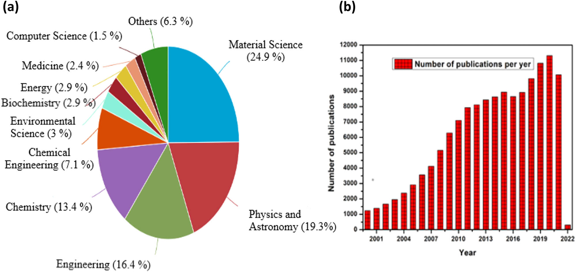
(a) Applicability of the ZnO in the different fields of science and technology and (b) number of publications per year related to ZnO.
2 Different methods for synthesis of ZnO nanostructures
Due to the diverse nature of structures acquired by the ZnO, the interest in knowing the physics and chemistry of these structures has increased drastically in recent years. These various structures attained by the nanometric ZnO make it a unique material with diverse set of characteristics and prospective uses in a variety of nanotechnology disciplines. ZnO occurs in one-dimensional (1-D), two-dimensional (2-D), and three-dimensional (3-D) structures [4]. 1-D group makes up the largest group, which includes NRs [61,62,63], needles [64], helixes, springs and rings [65], ribbons [66], tubes [67,68,69], belts [70], NWs [71,72,73], and combs [74]. The 2-D structures of ZnO include nanoplate/nanosheet and nanopellets [75,76]. 3-D structures are mainly flowers, dandelion, snowflakes, coniferous urchin-like, etc. [77,78,79,80]. Different techniques to produce various ZnO structures that differ in shape, size, and spatial arrangements are depicted in Figure 2. A detailed summary of ZnO obtained by different methods is given below in the Table 1.

Different synthesis methods used for the development of different ZnO structures.
Summary of different techniques for the fabrication of ZnO
| S. no. | Technique/method | Precursors | Characteristics and applications | Ref. |
|---|---|---|---|---|
| 1 | Precipitation process | Zn(CH3COO)2 and KOH as a solution | Particle diameter: 160–500 nm, BET: 4–16 m2/g | [81] |
| Zn(CH3COO)2 and (NH4)2CO3 | Zincite structure: spherical particles with a diameter of ∼30 nm | [82] | ||
| Application: used as a photocatalyst in photocatalytic degradation | ||||
| Zn(NO3)2 | Wurtzite structure with particle diameter ∼50 nm | [83] | ||
| Application: used in gas sensors | ||||
| Zn(NO3)2 and NaOH | Spherical size particles of around 40 nm | [84] | ||
| ZnSO4, NH4HCO3, and ethanol | Wurtzite structure with crystal size 9–20 nm and particle size diameter ∼12 nm | [85] | ||
| Zn(CH3COO)2 with NH3 as an aqueous solution | Particles with length ∼150 nm and diameter ∼200 nm | [86] | ||
| ZnSO4, NH4OH, and NH4HCO3 | Particle diameter ∼0.1–1 μm and length ∼60 nm | [87] | ||
| Micro-sized ZnO powder, NH4HCO3 | Hexagonal and wurtzite structure, flower, and rod-like shapes | [88] | ||
| Zn(CH3COO)2 and NaOH | Hexagonal structure with flower shape | [89] | ||
| Application: antimicrobial activity | ||||
| 2 | Sol–gel | Zinc acetate dihydrate, C2H2O4, C2H5OH, and CH3OH | Zincite structure, particles of rod-like shape with length ∼500 nm and diameter ∼100 nm | [90] |
| Application: used for decontamination of sarin | ||||
| Zinc acetate dihydrate, C2H2O4, and C2H5OH | Hexagonal wurtzite structure with uniformly spherical shaped particles | [91] | ||
| Zinc 2-ethylhexonate, ((CH3)4NOH), ethanol, and 2-propanol | Crystallites of cylindrical shape with diameter ∼25–30 nm and length 35–45 nm | [92] | ||
| Zinc acetate dihydrate, HN(CH2CH2OH)2, and C2H5OH | Hexagonal wurtize structure, particles possess the shape of nanotubes of the order ∼70 nm | [93] | ||
| 3 | Solvothermal hydrothermal and microwave techniques | ZnCl2 and NaOH | Particle morphology: bullet, rod-like (100–200 nm), sheet (50–200 nm), a polyhedron (200–400 nm), and so on | [94] |
| Zinc acetate (ZA) and sodium hydroxide | Spherical shape with particle diameter around 55–110 nm | [95] | ||
| ZA, zinc nitrate (ZN), lithium hydroxide, potassium hydroxide, and ammonium hydroxide | Hexagonal wurtize structure with microcrystallites size of the order of ∼100 nm to 20 μm | [96] | ||
| ZA, ammonia, C16H30O4Zn, C2H5OH, and C3H8O | Particles possess irregular ends along with holes, an aggregate of particles have a size of the order of 20–60 nm | [97] | ||
| Trimethylamine N-oxide, 4-picoline N-oxide, HCl, toluene, and ethylenediamine | Wurtzite structure with particle shape of NRs (40–185 nm) and NPs (24–60 nm) | [98] | ||
| ZA, ZN, C2H5OH, and imidazolium tetrafluoroborate ionic liquid | Hexagonal wurtize structure, hollow microspheres (2–5 μm) with nanosized particles, NRs (∼20 nm) along with flower-like microspheres | [99] | ||
| Zinc acetylacetonate, methoxy-ethoxy, and –butoxyethanol | Zincite structure with average crystal size ∼9–13 nm and diameter ∼40–200 nm | [100] | ||
| Zn(NO3)2 and deionized water | Hexagonal wurtize structure with NRs and NW shapes | [101] | ||
| Application: electronic and optical devices | ||||
| 4 | Emulsion | Zn(NO3)2 with surfactants | Size of grains: cationic surfactants ∼40–50 nm, nonionic surfactants ∼20–50 nm, and anionic surfactants ∼20 nm | [83] |
| Zn(C17H33COO)2, NaOH, decane, water, and ethanol | Morphology of particles: irregular particle aggregates with a needle, nearly spherical, and hexagonal shapes, along with spherical and pseudo spherical aggregates | [102] | ||
| Zn(CH3COO)2, heptane, and NH4OH | Hexagonal structure, spherical shape with particle diameter ∼0.05–0.15 μm | [103] | ||
| Zn(CH3COO)2, NaOH, KOH along cyclohexane, and nonionic surfactants | Hexagonal structure, particles show morphologies such as solids, ellipsoids, rods, flakes, and so on | [104] | ||
| Application: used as a photocatalyst | ||||
| 5 | Microemulsion | Zn(NO3)2, NaOH, heptane, hexanol, and Triton X-100 | Hexagonal wurtize structure with particle morphologies such as a needle (length ∼150–200 nm, diameter ∼55 nm) and nanocolumns (length ∼80–100 nm, diameter ∼50–80 nm) | [105] |
| Zn(NO3)2, oxalic acid, isooctane, benzene, ethanol, acetone, methanol, and so on | Spherical shape with diameter ∼11.7–12.9 nm and grain size ∼11–13 μm | [106] | ||
| Zn(CH3COO)2, aerosol OT, glycerol, n-heptane, NaOH, methanol, and chloroform | Hexagonal wurtize structure with the spherical shape of the order of ∼15–24 nm along with some rod shapes of length ∼66–72 nm and diameter ∼21–28 nm | [107] | ||
| ZnCl2, Zn(CH3COO)2, heptane, and so on | Hexagonal structure with uniformly dispersed particles of size ∼10 nm | [108] | ||
| 6 | Other methods | Zn(CH3COO)2 with thermal decomposition | Uniform size of particles ∼20–30 nm | [109] |
| Zn(NO3)2 with ultrasonic irradiation | Hexagonal wurtize structure with NRs and NW shapes | [101] | ||
| Application: used in electronic and optical devices | ||||
| ZnCl2, Na2CO3, NaCl with mechanochemical processing, and ZnO tetrapods by flame transport method | Hexagonal structure with a particle diameter of the order of ∼21–25 nm | [110] | ||
| An efficient way for the fabrication of tetrapod-like structures | [111,112] |
2.1 Sol–gel method
This technique has been prominently used for the fabrication of the ZnO because of its numerous benefits, such as ease of use, low cost, reliability, reproducibility, and very mild conditions of synthesis [4]. The efficient optical properties of ZnO NPs attained by this technique have remained a widely known topic of research as is observed due to the surge in the number of scientific publications [90]. The basic synthesis procedure for obtaining the films and powder by this method is shown in Figure 3 [113]. Figure 3(a) represents the method of obtaining the thin film from the colloidal sol, and Figure 3(b) illustrates the method of obtaining the powder form of ZnO from the colloidal sol by transforming it into a gel. Benhebal et al. [91] synthesized the ZnO powder by utilizing the precursors zinc acetate dehydrate and oxalic acid with ethanol as a solvent. The powder form of the ZnO was then characterized using X-ray diffraction, nitrogen adsorption isotherms, scanning electron microscopy, and UV-Vis spectroscopy. It has been found that the powder possesses the hexagonal wurtzite structure with spherical-shaped particles. The surface area was found to be 10 m2/g by using Brunauer-Emmett-Teller (BET) equation. Ristic et al. [92] utilized this method for obtaining nanocrystalline ZnO. Yue et al. [93] produced the ZnO by using the sol–gel technique. Finally, it is also worth to mention that incorporating the anodic aluminum oxide membrane with a sol–gel technique will help to synthesize high-quality 1-D nanomaterials along with the extension of its applications as a template for the development of nanostructures.
![Figure 3
Two examples of synthesis of ZnO by sol–gel method: (a) film of ZnO from colloidal solution and (b) powder form of ZnO from gel. Reproduced with permission from Elsevier [113].](/document/doi/10.1515/ntrev-2022-0035/asset/graphic/j_ntrev-2022-0035_fig_003.jpg)
Two examples of synthesis of ZnO by sol–gel method: (a) film of ZnO from colloidal solution and (b) powder form of ZnO from gel. Reproduced with permission from Elsevier [113].
2.2 Emulsion or microemulsion method
The emulsion is defined as a liquid phase in which another discontinuous and immiscible liquid phase is dispersed. Emulsions are usually classified based on the nature of the external phase; one group is called “oil-in-water,” and another one is called “water-in-oil.” The terms “oil” and “water” are very well known with their general definitions as any highly polar hydrophilic liquid belongs to the category of “water,” whereas hydrophobic and nonpolar liquids belong to “oil” group [104,105]. Vorobyova et al. [102] applied the technique of emulsion for synthesizing the ZnO. They obtained the ZnO by performing a reaction between zinc oleate dissolved in water with sodium hydroxide. The study revealed that processing conditions such as temperature, substrates, and the ratio of two phase components impact the particle size along with their phases. The obtained ZnO had different particle shapes such as near-spherical, near-hexagonal, and spherical aggregates. Lu and Yeh [103] also obtained ZnO by applying the emulsion technique. In a similar fashion, many researchers obtained the ZnO by the phenomenon of precipitation in an emulsion system. In these systems, ZA is being used as a precursor along with sodium hydroxide or potassium hydroxide as a precipitating agent [104]. Microemulsion are stable and isotropic liquids that consist of two different layers along with surfactant. It has been observed that the size drop on microemulsion is relatively small, lies within the range 0.0015–0.15 μm [114]. Furthermore, microemulsion are spontaneous in comparison to the emulsion technique. Li et al. [105] synthesized the nanometric form of ZnO by microemulsion technique. They obtained the ZnO by adding the alcohol to the emulsion system which consists of water, oil, and emulsifier. During the synthesis of NPs, the exchange process took place among substrates, microemulsion droplets, and medium in an aggregation of the formed nuclei. In the whole synthesis process, different concentrations of the polyethylene glycol 400 were used. Similarly, many researchers have used this method for the fabrication of ZnO [83,106,107,108].
In addition to the above-mentioned well-known methods, there are many other methods to synthesize ZnO such as pyrolysis spray method, sonochemical method, microwave method, and developing ZnO from the gas phase. ZnO nanostructures were prepared from an aqueous solution of ZA (Zn(CH3COO)2.2H2O) and hydrazine hydrate (N2H4) [115]. These precursor solutions were mixed with distilled water under vigorous stirring while a N2H4 solution was added drop-wise into the solution and then transferred into a 100 mL Teflon liner and finally subjected to microwave (Perkin Elmer/Anton Paar Multiwave 3000) oven irradiation at 150 W microwave power for 10 min. The resulting white precipitate at the bottom of the Teflon was collected, filtered, and then washed several times with absolute ethanol and distilled water to remove any impurities and then dried. Violet-blue emitting ZnO nanostructures were obtained by this method. The electron spin resonance signal was also found to gradually decrease with increasing annealing temperature signifying the decrease in the concentration of zinc interstitials (Zni’s) and/or zinc vacancies (VZn’s) defects in the ZnO nanostructures. Similarly, Zhao et al. [109] utilized the pyrolysis method and obtained the ultrapure ZnO particles. They used zinc acetate dehydrate as a precursor because of its high solubility and decomposition temperature. From the analysis, it has been observed that the water of crystallization gets lost below 200°C, and anhydrous ZA starts to develop. Then by slowly increasing the temperature up to 400°C both endothermic and exothermic reactions take place, which results in the decomposition of the ZA into ZnO and some organic compounds. Hu et al. [101] suggested the growth of ZnO rods by the sonochemical process and microwave heating. According to them, ZnO synthesis in this way does not require any surfactant along with its simple and energy-efficient nature. Also, this method can be used in large scale with minimum production costs. The ZnO NRs find applications in electronics and optoelectronic devices. Salman et al. [116] obtained the controlled growth and morphology of ZnO in nanostructures by applying the domestic microwave synthesis. Grasza et al. [117] obtained the pure crystals of ZnO by growing it from a gas phase medium, using broad range of values for heating time and temperature. They observed that heating in gaseous zinc results in surface roughness of less than 1 nm, compared to the heating in gaseous arsenic, which leads to the deterioration of the crystal surface. Moreover, by increasing the temperature and the heating time, improved porosity of the surface was observed. The PLD method was used by Wei et al. [118] for the ZnO fabrication.
3 Structural Informations
Structurally, ZnO is mainly found in three different types of unit cells, namely hexagonal wurtzite, zinc blend, and rock salt, as shown in Figure 4 [6,119].
![Figure 4
(a) The hexagonal wurtzite structure of ZnO, (b) the rock-salt, and (c) zinc blende phases of ZnO. O atoms are shown as white spheres, and Zn atoms are shown as black spheres. Only one-unit cell is illustrated for clarity. Reproduced with permission from Elsevier [119].](/document/doi/10.1515/ntrev-2022-0035/asset/graphic/j_ntrev-2022-0035_fig_004.jpg)
(a) The hexagonal wurtzite structure of ZnO, (b) the rock-salt, and (c) zinc blende phases of ZnO. O atoms are shown as white spheres, and Zn atoms are shown as black spheres. Only one-unit cell is illustrated for clarity. Reproduced with permission from Elsevier [119].
Among these, the hexagonal wurtzite is well known because of its stability at RT and normal atmospheric pressure [6]. It is composed of triangularly stacked alternate biatomic close-packed planes where-in four zinc ions (Zn2+) are located at corners, with oxygen ion (O2−) placed at the center and vice versa. The zinc and oxygen ions are thus arranged in the manner of AaBbAaBb…in the <0001> direction within a plane [6,12]. The structure of the zinc blend is metastable. Because of its stability, it is difficult to grow it, as it possesses the stability only in a cubic structure [6,12]. For stabilization, it is usually developed on cubic substrates, such as ZnS [120], GaAs/ZnS [121], and Pt/Ti/SiO2/Si [122], which depicts the compatibility to overcome the innate approach regarding the formation of the wurtzite phase. The symmetry of zinc blend structure is given by space group F4̄3m in the Hermann–Mauguin representation and also possess two interpenetrating face-centered cubic structure [123]. In contrast to wurtzite, the atoms are arranged in the stacking order of AaBbCcAaBbCc…within a plane. In the case of rock-salt, both the zinc and oxygen atoms remain surrounded by their six nearest neighboring atoms. It possesses its stability only at higher pressure (<10 GPa) and is also epitaxially unstable [6]. It has also been found that the rock-salt structure of ZnO can be acquired from the hexagonal wurtzite structure on the application of high pressure [124]. Among the above structures of ZnO, the stable wurtzite structure has been studied to a large extent on both experimental and theoretical grounds. Some of the observed pressure parameters of ZnO structure are presented in Table 2.
Experimental and theoretical pressure parameters of ZnO
| Experimental results | Theoretical results | ||||||||
|---|---|---|---|---|---|---|---|---|---|
| Wurtzite volume (A3) | Rock-salt volume (A3) | ∆V/V (%) | Transition pressure P tr (GPa) | References | Wurtzite volume (A3) | Rock-salt volume (A3) | ∆V/V (%) | Transition pressure P tr (GPa) | Ref. |
| 23.829 | 19.60 | 16.7 | 9.5 | [125] | 23.346 | 19.515 | 16.41 | 9.32 | [126] |
| — | 19.40 | — | 9.0 | [12] | 24.570 | 19.799 | 19.42 | 8.57 | [127] |
| 23.796 | 19.484 | 18.13 | 8.7 | [128] | 23.62 | 19.08 | 18.8 | 8.0 | [129] |
| 23.785 | 19.60 | 18.0 | 10.0 | [130] | 17.9 | 14.5 | [128] | ||
| 23.81 | 19.60 | 17.68 | 9.1 | [131] | 23.839 | 19.041 | 20.3 | 10.45 | [132] |
4 Properties of ZnO
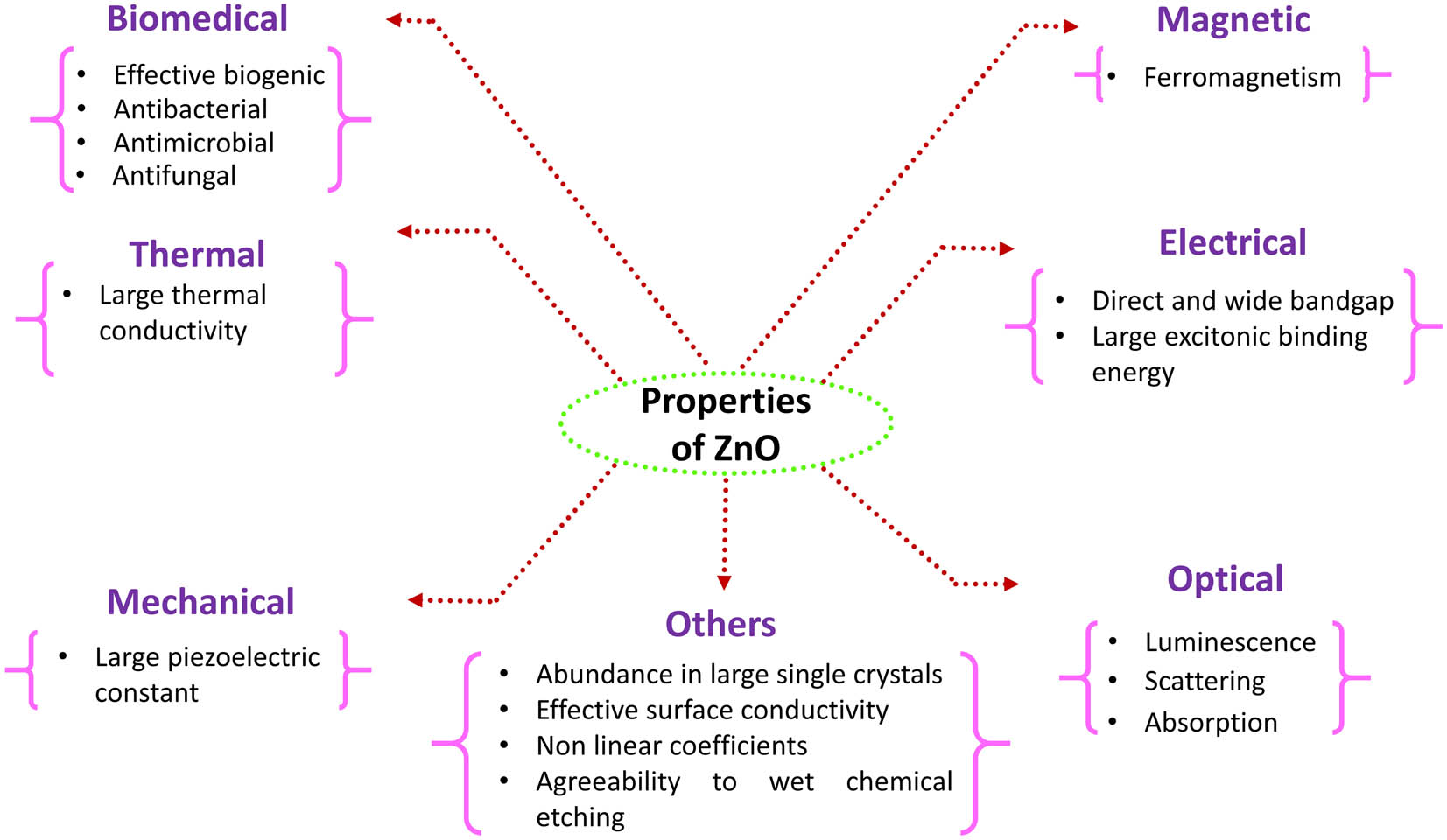
The wide range of beneficial characteristics showed by ZnO has been recognized in the past decades [7]. ZnO belongs to the direct and wide bandgap (∼3.37 eV) metal oxide semiconductor family and is a very astonishing material to be suitable for a large number of technological applications [6,13]. The possibility of such utilities has been filled by significant advancement in bulk-crystals [37,133] along with the thin-film development in recent years [134,135,136,137,138,139]. ZnO has a number of characteristics that differentiate it from other oxides and makes it valuable for different applications. These characteristic properties can be explained directly or can be categorized based on their nature, that is, electrical, optical, mechanical, magnetic, thermal, etc. These properties attribute an abundance of applications to the ZnO. Figure 5 represents the different properties of the ZnO, followed by their brief explanation as well.
Categorization of properties on the basis of their nature.
4.1 Electrical properties
The bandgap of ZnO is 3.44 eV at low temperature and 3.37 eV at ambient temperature [140]. For comparison, the specific characteristic of wurtzite GaN at low and RTs are 3.50 and 3.44 eV, respectively [141]. These properties broaden its applications for optoelectronic devices in the blue/UV regions, including LEDs, laser diodes, and photodetectors [12,23]. Moreover, the optically lasing action has been noticed in ZnO platelets, thin films, a group composed of nanocrystal of ZnO, and in ZnO NWs [16,17,142,143]. Also, applications with regard to p–n homojunction have been reported, however, security and reproducibility have not been set up yet [144,145,146]. Also the free-exciton binding energy in ZnO is 60 meV [16,17], in comparison with 25 meV in GaN [141]. This huge exciton binding energy shows a proficient excitonic emission in ZnO and can endure at both room and higher temperatures [16,17]. As the excitonic strength of the oscillators is significantly greater in comparison to the direct electron–hole transitions in direct gap semiconductors, the enormous exciton binding energy of ZnO makes it an efficient material for optical gadgets that rely on excitonic impacts [147].
4.2 Optical property
In general, the visible luminescence arises due to the recombination of the deep level defects, that is, so-called deep level emission. These imperfections are generally the consequences of several factors, such as crystal perfection, surface morphology, stoichiometry deviation of the material, and doping and impurities. [148,149]. Because of the high luminosity in the green–white range of the spectrum, ZnO is, additionally, an efficient material for phosphor applications. The emission spectrum of the ZnO has a peak at 495 nm and an extremely wide half-width of the order of 0.4 eV. The broad green luminescence possesses its center in between 2.4 and 2.5 eV [150,151,152]. The phenomenon of green luminescence has been observed in samples synthesized by different methods, it is still not completely understood whether native defects are the origin of green emission, and if they are, which defects are accountable. For example, the occurrence of Cu debasements has been proposed as a possible explanation [153,154], but it has been observed that Cu is not present in all the samples of ZnO that have been studied for the green luminescence. Local imperfections have been proposed as an expected cause for the mentioned phenomenon. It has been reported that VZn enhances green luminescence [150,151,155]. For the proper explanation of this phenomenon, different interpretations have been suggested by the researchers. Some researchers have recommended that the green luminescence arises because of the oxygen vacancies (Vo’s) [156,157,158,159,160,161,162]. Pramanik et al. [163] have recently investigated the effect of Vo’s on the photoluminescent property of the ZnO. They observed that with the increase in the synthesis time, both the band gap and the PL intensity start decreasing. The string green emission has been observed at approximately 540 nm, whereas blue emission has been observed at 485 nm. They also observed the shift in the emission by changing the band gap excitations. The PL spectra recorded for the samples synthesized with a slight difference in their preparation time and the CIE diagram for visualization of the emission colors are shown in Figure 6. Besides different explanations, some researches have also studied the effect on the emission intensity due to change in the number of the Vo’s [158,162,163,164]. Their argument related to the Vo’s availability depends on the perception of a line with g ∼ 1.96 in electron paramagnetic resonance (EPR) estimation [158,162].
![Figure 6
Excitation wavelength-dependent normalized PL spectra corresponding to the samples grown for microwave synthesis time of (a) 1 min, (b) 2 min, and (c) 4 min. Insets show the variation of integrated visible PL intensities as a function of excitation wavelength for all the samples. (d) Color chromaticity diagram for the sample corresponding to (a). Reproduced with permission from Elsevier [163].](/document/doi/10.1515/ntrev-2022-0035/asset/graphic/j_ntrev-2022-0035_fig_006.jpg)
Excitation wavelength-dependent normalized PL spectra corresponding to the samples grown for microwave synthesis time of (a) 1 min, (b) 2 min, and (c) 4 min. Insets show the variation of integrated visible PL intensities as a function of excitation wavelength for all the samples. (d) Color chromaticity diagram for the sample corresponding to (a). Reproduced with permission from Elsevier [163].
In addition, ZnO is a potential material for applications in vacuum fluorescent displays and field emission displays because of its n-type conductivity nature. The inception of luminescence centers and the luminescence mechanism are not so much comprehended, ascribed to Vo’s or Zni’s, with no reasonable proof. Because these imperfections cannot transmit in the green regions, it has been proposed that VZn’s are an almost certain reason for the green glow. VZn’s are acceptors and prone to form in n-type ZnO [165]. Kumar et al. [166] with the help of X-ray photoelectron spectroscopy (XPS) and PL, demonstrated that the emission from ZnO is directly related to the defects in the ZnO. ZnO nanophosphors (ZnO NPr) were synthesized by a combustion method using ZN and ZA as precursors and urea as a fuel. UV and orange-red light were emitted due to different defects in the NPrs. XPS showed that the O 1s peak consists out of three components: O1 (ZnO), O2 (deficient oxygen; OH groups), and O3 (adsorbed species), respectively, as shown in Figure 7. The O2 is linked with O2− ions in oxygen-deficient regions within the matrix of ZnO and/or Zn–OH groups. Hence, variation in the intensity of this part may be somewhat linked to the variation in the concentration of oxygen vacancies (Vo). The relative intensity of the O2 peak is much higher for the ZN in comparison to ZA sample, meaning that the concentration of oxygen defect is higher in the case of the ZN. This effect was confirmed with the broad orange-red emission from 500 to 850 nm that was obtained from the ZnO NPr synthesized with the ZN precursor. The observed phenomenon may be ascribed to different kinds of defects, and a sharp UV band, due to the passivation of defects, at 392 nm from ZnO NPr prepared with the zinc acetate precursor, as shown in Figure 8. A possible schematic energy diagram was drawn from the observed data is shown in Figure 8(c). The band transition from Zni to Oi level, Zni to Vo level and Vo to valence band is obtained at ∼2.06, 1.43, and 1.51 eV, respectively.
![Figure 7
O 1s XPS peak of ZnO NPs before and after Ar+ sputtering. Reproduced with permission from Elsevier [166].](/document/doi/10.1515/ntrev-2022-0035/asset/graphic/j_ntrev-2022-0035_fig_007.jpg)
O 1s XPS peak of ZnO NPs before and after Ar+ sputtering. Reproduced with permission from Elsevier [166].
![Figure 8
(a) PL spectra of the different ZnO NPr, (b) and (c) are the deconvoluted peaks of the broad band PL spectra, and (d) schematic energy band diagram of PL spectra. Reproduced with permission from Elsevier [166].](/document/doi/10.1515/ntrev-2022-0035/asset/graphic/j_ntrev-2022-0035_fig_008.jpg)
(a) PL spectra of the different ZnO NPr, (b) and (c) are the deconvoluted peaks of the broad band PL spectra, and (d) schematic energy band diagram of PL spectra. Reproduced with permission from Elsevier [166].
4.3 Thermal property
The characteristic of large thermal conductivity in ZnO has made it valuable for an added substance; that is, ZnO is added to elastic for the expansion of the thermal conductivity of tires. High thermal conductivity converts into enhanced proficiency of heat expulsion amid gadget activity [167,168]. Besides this, the semiconductor gadget creation measures incredibly advantage due to the agreeability to wet chemical etching at low temperature. Furthermore, the studies have revealed that ZnO thin films can be incised with an acidic, alkaline, and also by a mixture of solutions. This chance of low-temperature chemical etching provides incredible adaptability for the preparation, planning, and integration of electronic and optoelectronic gadgets [7]. Also, for the examination of the high power and high temperature electronic and optoelectronic devices, the thermal conductivity, governed by the contribution of the rotational, vibrational, along with the electronic degrees of freedom, is an incredibly essential material characteristic. The phonon–phonon scattering acts as a limiting mechanism for the thermal conductivity in pure crystals, which is inversely related to temperature. The phonon–phonon Umklapp scattering and phonon scattering by point and extended defects dominated the heat transmission. Similar to the existence of thermal conductivity due to imperfection in other semiconductors, the defects have a crucial role in the thermal conductivity shown by ZnO [168].
4.4 Mechanical property
In piezoelectric materials, an imparted voltage distorts the crystal and vice versa. These materials are commonly utilized as sensors, transducers, and actuators. The weak symmetry of the wurtzite crystal structure joined with an enormous electromechanical coupling in ZnO offers ascend to effective piezoelectric and pyroelectric characteristics. Piezoelectric ZnO films with consistent thickness and direction have been developed on various substrates utilizing distinctive deposition methods, that is, sol–gel, spray pyrolysis, chemical vapor deposition, molecular-beam epitaxy, etc. [157,169,170,171,172,173,174,175]. Because of this piezoelectric property offered by the ZnO thin films, they are largely being used in the development of different types of micro electrochemical systems (MEMs). Tao et al. [176] have utilized the ZnO thin film synthesized by using the sputtering method for the fabrication of two-degree-of-freedom (2DOF) MEMS piezoelectric-vibration energy harvester chip. The design procedure they followed for the development of the MEMs is shown in Figure 9. The fabricated device has been found to possess the piezoelectric coefficient of the order of 4.66 pc/N. For the confirmation of the percentage composition of the different elements, the energy dispersive X-ray spectroscopic studies have also been performed. The studies confirmed the presence of oxygen, silicon, zinc, and platinum with 53.98, 26.48, 17.91, and 18.37%, respectively.
![Figure 9
Procedure for the development of the 2DOF MEMs based on the ZnO. Reproduced with permission from Elsevier [176]. (a) Patterning Pt/Au bottom electrode through a lift-off process, (b) spin-coating photoresist and followed by lithography, (c) deposition of ZnO by sputtering at room temperature, (d) remove photoresist by wet etching, (e) deposition of Pt/Au top electrode, (f) patterning SiO2 by RIE, (g) frontside feature patterning through lithography and DRIE process, and (h) backside feature patterning and realease the structure.](/document/doi/10.1515/ntrev-2022-0035/asset/graphic/j_ntrev-2022-0035_fig_009.jpg)
Procedure for the development of the 2DOF MEMs based on the ZnO. Reproduced with permission from Elsevier [176]. (a) Patterning Pt/Au bottom electrode through a lift-off process, (b) spin-coating photoresist and followed by lithography, (c) deposition of ZnO by sputtering at room temperature, (d) remove photoresist by wet etching, (e) deposition of Pt/Au top electrode, (f) patterning SiO2 by RIE, (g) frontside feature patterning through lithography and DRIE process, and (h) backside feature patterning and realease the structure.
As the piezoelectricity property enables the materials to transform the mechanical energy into electrical energy and vice versa, which makes them extremely interesting because of solving the energy concern shortly. As a result, materials that possess high piezoelectric coefficients are being found as an intriguing study area for researchers. In this regard, the ZnO also has gained increasing focus as a significant semiconductor because of its large piezoelectric coefficient among the II–VI compounds. In comparison to other compounds of the same group (ZnS, CdS, etc.), it has been found that the piezoelectric tensor of ZnO is two times that the rest [177]. At the very first in 1994, Dal Corso et al. [178] used the ab initio approaches for the evaluation of the piezoelectric constant of ZnO. According to their calculations, they concluded that the strong piezoelectric behavior is due to its low clamped-ion contribution. Similarly, Hill and Waghmare [179] used the first-principle simulations for the investigation of the effects of stress and temperature on the piezoelectric property of ZnO. They observed that the piezoelectric constant is substantially influenced by both stress and temperature conditions. This dependence on stress and temperature is very critical for future applications as fine-tuning of piezoelectric characteristics for specific device applications may be accomplished by controlling the ZnO lattice constants. Due to rapid progress in electronic technology, low-dimensional nanostructures, that is, NWs and nanofilms, have received greater attention in recent years due to their potential uses in nanoscale electronics. Immense attention has been diverted toward the ZnO NW as they act as key components in most of the MEMS. It was for the first time in 2006 when first-principle calculations were used for investigating the piezoelectricity of hexagonal (0001) nonpassivated ZnO NWs with diameters up to 2.8 nm. It has been observed that because of the free boundary, ZnO NWs possess a higher effective piezoelectric constant than bulk ZnO [180]. Besides the theoretical, experimental studies have also been carried out on the piezoelectric behavior of ZnO. Wacogne et al. [181] have investigated the piezoelectric characteristics of ZnO films experimentally. The key components of their studies were substrate temperature, optical loss, radio-frequency electrical activity, etc. Von Preissig and his coworkers [182] developed a novel technique for determining the piezoelectric strength of ZnO thin films for MEMS application.
4.5 Magnetic property
ZnO is currently being investigated for the ferromagnetic behavior at RT that has been observed in the pure semiconductor. The genesis of this property observed in the undoped ZnO is still a matter of debate [183,184,185,186,187]. Most of the researchers have reported that this property arises due to the presence of Vo’s in the ZnO [186,188,189]. Panigrahy et al. [186] investigated the ferromagnetic characteristic of ZnO that possesses different Vo concentrations and observed the changes by altering the different synthesizing parameters, such as growth time and annealing time. They observed a reduction in the magnetization as the size and the annealing temperature of NRs has been increased, owing due to a decrease in the defect-related emission from the singly charged Vo. They conclude that the concentration of the Vo and magnetization are directly interrelated to each other. Xu and coworkers [190] recommended that the single charge Vo positioned close to the surface play an essential function in modulating ferromagnetism in undoped ZnO NPs. Some researchers have also investigated the antiferromagnetism in undoped ZnO synthesized via the wet chemical technique at an ambient temperature. The investigations have revealed that the magnetic property of the ZnO is strongly correlated with the concentration of Vo at the surface [190].
4.6 Biomedical property
In the previous years, when contrasted with other metal oxides, it has been observed that ZnO provides an environment hostile to bacterial properties, because of which it acts as a hotbed for the researches. ZnO nanostructures have demonstrated more toxic behavior against microorganisms and are less receptive to human cells [191,192,193,194], as in ZnO nanostructures reactive oxygen species (ROS) enables it for the antibacterial action, as it eliminates the bacterial cell [195,196,197,198,199]. The main aim of the ROS is to prevent humans from infectious diseases and utilize the technological agents, which are easy to produce, green, simply transported, economical, and influenced by bio-film morphology, hence proves to be useful for humans [200,201]. The basic principle of ZnO nanostructures is dubious yet [202]; however, numerous investigations have announced the antibacterial systems of ZnO structures wherein the ROS and response among nanostructures and bacterial cells damages the entire cell and lead to the freedom of Zn2+ particles [191,195,197,198,203,204]. Most researchers have reported that ROS provides the main mechanism of nanotoxicity [195,196,197,198,199,205]. ZnO nanostructures have been accounted as a dominant inhibitor of bacterial thriving because of ROS creation and release of Zn2+ ions, which harms the cell wall and causes cell death [206,207,208,209]. Most of the metal oxides act as a suitable antibacterial agent because of ROS production, which results in the formation of O2−, OH−, and H2O2 [205,207]. The antibacterial proficiency of ZnO nanostructures unequivocally relies on the size of nanostructures. There is an effective increment in the surface-to-volume proportion as the size of the ZnO nanostructures diminishes, thus improving the surface area when contrasted with volume, and ROS creation depends directly upon the surface area of ZnO nanostructures [196,210]. Also, an efficient increase occurs in ROS production when the concentration of the ZnO starts rising [211]. Furthermore, the difference between the electrical potential of the medium and external surface of the microbes, so-called the zeta-potential is altogether influenced by the concentration of nanostructures that legitimately influences ROS creation [212]. Ongoing research has additionally revealed that the presence of ZnO nanostructures brings about direct associations and efficient bindings to bacterial cells and can harm the cell membrane, which results in the death of cells through apoptosis [192,197]. Such type of research has been broadly revealed by numerous specialists around the world against a few miniature living beings. Furthermore, the antibacterial properties of ZnO nanostructures, along with their shape, size, and tested micro-organisms was reported by the various researchers [213,214,215,216,217,218,219,220,221,222,223,224].
4.7 Other properties
Besides the above-mentioned characteristics features, the exceptional high radiation hardness greater than GaN shown by the ZnO is very crucial for different purposes at high altitudes or in space. Also, it is possible to alter the bandgap of ZnO by adding magnesium or cadmium as is done in some GaN-based alloys [225,226,227,228,229,230]. Furthermore, in comparison with the amorphous silica or organic semiconductors ZnO ways out the options for the fabrication of thin-film transistors on flexible substrates with enhanced electron mobility [231,232]. Other important properties of the ZnO are also briefly explained in sections 4.7.1, 4.7.2 and 4.7.3.
4.7.1 Abundance in large single crystals
Large single crystals are being fabricated with various methods, comprising hydrothermal growth, vapor-phase transport, and pressurized melt development [37,133,233,234,235]. The epitaxial development of ZnO on local substrates can prompt top-notch thin films with a decreased level of extended defects. This has been found effective when contrasted with GaN, for which local substrates do not exist. Considering how the GaN-based gadgets have accomplished high efficiencies irrespective of the moderately huge concentration of expanded imperfections, it is conceivable that a high-quality ZnO-based gadget could outperform the efficiencies acquired with GaN [136,137,138,139,206,236].
4.7.2 Effective surface conductivity
The thin films fabricated from ZnO via different methods possess a very sensitive nature if their surface gets exposed to gases. It may be used as a low-cost odor sensor able to sense the freshness of foods and drinks, owing to its prominent sensitivity to trimethylamine present in the odor. The working of the sensor action is not fully understood. Recent investigations uncovered the existence of an electron layer buildup on the surface in vacuum-tempered single crystal, which vanishes when the material is exposed to encompassing air. This layer may also assume a function in the sensor activity [237,238,239].
Recently, the EPR measurements were performed for proper understanding of the intrinsic defects at different temperatures. The researchers have observed that the occurrence of the defects on the surface has a significant role in conducting the behavior of ZnO. Most interestingly, it has been observed that at 300°C, only surface defects became evident in the EPR spectra of ZnO nanocrystals, which eventually favors the p-type conductivity [240].
4.7.3 Nonlinear coefficients
The linear and nonlinear optical characteristics of any semiconductor are very important from both the theoretical and the experimental point of view [241]. Especially, the nonlinear optical coefficients are significant factors for comprehending the physics of nonlinear optical processes [242]. The unique features shown by the nanosemiconductors in comparison to their bulk equivalents have piqued attracted both the fundamental and the technological researchers [243]. The efficiency of the wavelength-conversion devices relies on the nonlinear optical coefficients. Among a large number of semiconductors, the appealing nonlinear feature of ZnO has made it a good candidate for the nonlinear optical device fabrication. The nonlinear optical characteristics in nanocrystals have been studied at both the quantum confinement effects, that is, weak and strong-confinement regimes. The theoretical and experimental studies have revealed that the state-filling effect is responsible for the nonlinearity in the regime of strong confinement. In this regime, the state-filling effect acts in such a way that both the photoexcited electrons and hole get independently confined [244]. In the case of the weak confinement regime, the Coulomb interaction in-between the electron and the hole produces an exciton, which is confined as a quasiparticle. The size-dependent amplifications of the nonlinear susceptibility have also been examined both theoretically and experimentally, and it has been observed that the exciton–exciton interactions are mainly responsible for the nonlinearity, which in turn leads to the divergence from the harmony of the boson-like exciton within the nanocrystal [243]. Furthermore, the ZnO crystals and, specifically, thin films reveal nonlinear optical activity at the second-and third-order, which has been found useful for nonlinear optical gadgets. The nonlinear optical effects in ZnO thin films proves to be beneficial for integrating nonlinear optical gadgets [245].
5 Native defects in ZnO
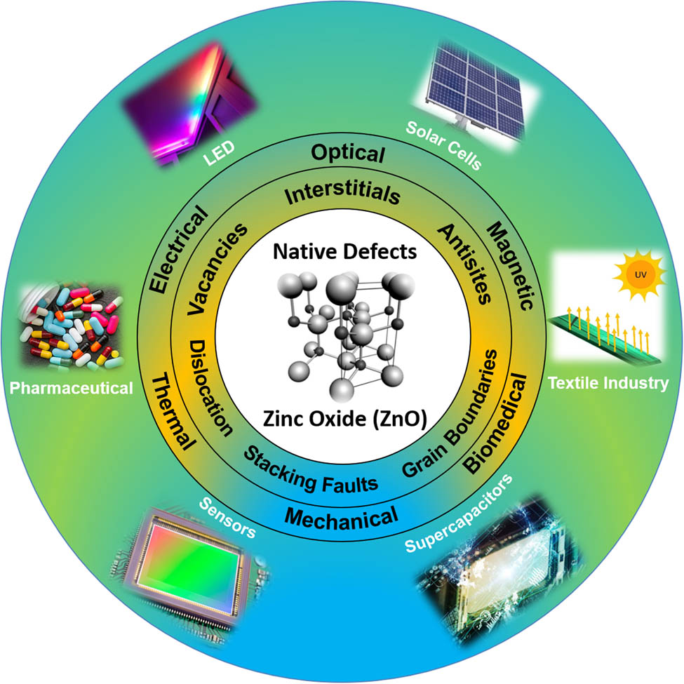
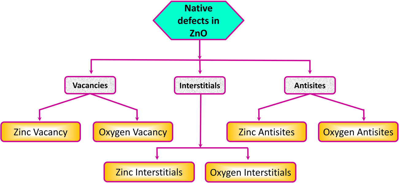
The development of nanotechnology has opened up large number of possibilities for manipulating the ZnO structures on all dimensions and broadens its application field. Besides some inherent defects that are very much responsible for the different properties, engineering the ZnO nanostructures with regulated dimensions, size, porosity, crystal aspects, and mesoscale geometries has greatly improved their performance for variety of applications [246,247]. The local or intrinsic or native deformities are the blemishes in the crystal lattice that include just the constituent components [7]. ZnO mainly possesses six types of defects, that is, vacancies, interstitials, and antisites (a “Zn” molecule involving an “O” lattice site or vice-versa), which are pictorially represented in Figure 10 [8,248]. Defects such as Vo’s have low formation enthalpies in p-type ZnO and are therefore expected to form readily [156].
Different types of defects found in ZnO.
Although they may assume a noteworthy part as compensating centers, Vo’s and other native point defects are assumed to be the main cause of the unintentional n-type conductivity in ZnO [155]. Discussion regarding defects in ZnO primarily concerns their nonstoichiometry and n-type conductivity behavior. In early studies, both experimentally and theoretically, it was assumed that only Zni’s and Vo’s are the only defects responsible for the above-mentioned property; however, it was unable to explain many of the other phenomenon [249,250]. Later on, first principle study provides deep insights regarding the energetics, atomic, and electronic structure of these native defects [6,57,59,155,156,251–263]. Most studies have inferred that the Zni has a high arrangement vitality, although it is a shallow donor. The “O” vacancy has a low arrangement vitality, yet it is a profound donor that cannot produce a high concentration of carrier electrons. Subsequently, neither Zni nor Vo is a probable wellspring of n-type conductivity. A few different competitors have proposed based on the first-principle study: the “H” impurity unexpectedly incorporated into an interstitial site (OH− – like arrangement) or into the oxygen site [55,264], a metastable shallow donor for the Vo, a complex of a Zni and “N” contamination, along with Zni balanced out within the sight of a high concentration of the Vo [258,260,265]. Local deformities are, by and large, identified with the remuneration of the dominating acceptor or donor dopants. For example, it is simple to create donor defects in p-type material, although acceptor defects are simpler to frame in n-type material, every time counteracting the prevailing conductivity. Local deformities have been accepted to play a significantly more significant function in ZnO, which regularly shows elevated levels of accidental n-type conductivity. Vo’s and Zni’s have been frequently conjured as wellsprings of n-type conductivity in ZnO [249,266–269]. In general, the native deformities influence the exhibition of Ohmic and Schottky contacts. Depth-resolved cathodoluminescence uncovered the arrangement of point defects at metal-ZnO interfaces, prompting modifications in the Schottky barrier characteristics [270].
5.1 Oxygen vacancies
The oxygen vacancy is among the most referenced deformity in the ZnO literature; it is consequently advantageous to committing extraordinary consideration regarding this imperfection. The Vo has been frequently invoked as the wellspring of accidental n-type conductivity [7]. Even though the Vo has the most minimal formation energy among the imperfections that act as donors as depicted in Figure 11, the calculations performed via computational methods demonstrate that the Vo is an exceptionally very deep rather than a shallow benefactor and, thus, cannot add to an n-type conductivity [57,58,263]. Though the calculations available in the published data vary on the values for transition levels and formation energies because of the various methods to precise the band gap, they solidly agree that oxygen vacancy is a deep donor [57–59,156,251,252,259].
![Figure 11
(Color online) Formation energies as a function of Fermi-level position for native point defects in ZnO. Results for Zn-rich and O-rich conditions are shown. The zero of Fermi level corresponds to the valence-band maximum. Only segments corresponding to the lowest-energy charge states are shown. The slope of these segments indicates the charge state. Kinks in the curves indicate transitions between different charge states. Reproduced with permission from Elsevier [263].](/document/doi/10.1515/ntrev-2022-0035/asset/graphic/j_ntrev-2022-0035_fig_011.jpg)
(Color online) Formation energies as a function of Fermi-level position for native point defects in ZnO. Results for Zn-rich and O-rich conditions are shown. The zero of Fermi level corresponds to the valence-band maximum. Only segments corresponding to the lowest-energy charge states are shown. The slope of these segments indicates the charge state. Kinks in the curves indicate transitions between different charge states. Reproduced with permission from Elsevier [263].
First-principle counts reliably reveal that the Vo is a profound, negative-U contributor, where the 1+ charge state is thermodynamically flimsy. It has been observed that when the Fermi energy is over the “0/2+ level,” the imperfection is in the unbiased charge state. When the Fermi energy is beneath the “0/2+” level, the deformity has a charge of “ +2e.” The “0/2+” level of the Vo has been determined to be at 0.5–0.8 eV over the valence-band maximum [251,255,257,259,271]. Calculations that endeavor to address the bandgap blunder of the local density approximation assessed the “0/2+” level to be 1–2 eV underneath the conduction-band minimum. The determined movement obstruction for the unbiased Vo is ∼2 eV. Precisely, whether oxygen vacancy is primarily accountable for the n-type conductivity in ZnO has been still unsettled for the past 50 years. For instance, Lany and Zunger [259] anticipated groupings of 1017/cm3 or higher, whereas Janotti and Van de Walle [263] estimated that the formation energy is excessively high for noteworthy fixations to exist at balance. One can comprehend that Vo’s electronic structure in ZnO depends on a straightforward model inside molecular orbital theory (MOT) that includes the four Zn hanging bonds (sp3 hybridization) and two electrons.
These Zn hanging bonds join into a completely symmetric “a1” state, which remains in the bandgap, and three partially degenerate states in the conduction band. In the unbiased charge condition of the Vo, the “a1” state is doubly involved, and the three states in the conduction band are unfilled. The control of the “a1” state is legitimately identified with the neighborhood cross section unwinding around the Vo. In the neutral charge express, the four zinc atoms firmly loosen up internal (around the vacancy) by 12% of the balance Zn–O bond length. In the “+1” charge state, they marginally loosen up outward by 3%; and in the “+2” charge state, the four zinc atoms unequivocally loosen up outward by 23% as shown in Figure 12 [7,57]. The observed significant difference in relaxations leads to the decrease in the formation energy of different charge states of oxygen such as
![Figure 12
(a) The atomic relaxations surrounding the oxygen vacancy in different charge states. For each charge state’s equilibrium configuration, the location of the a1 state is also displayed. (b) Presence of Fermi energy in different charge states at conduction band minimal. (c) Presence of Fermi energy in different charge states at valence band maximum. Reproduced with permission from Elsevier [57].](/document/doi/10.1515/ntrev-2022-0035/asset/graphic/j_ntrev-2022-0035_fig_012.jpg)
(a) The atomic relaxations surrounding the oxygen vacancy in different charge states. For each charge state’s equilibrium configuration, the location of the a1 state is also displayed. (b) Presence of Fermi energy in different charge states at conduction band minimal. (c) Presence of Fermi energy in different charge states at valence band maximum. Reproduced with permission from Elsevier [57].
Currently, the majority of the trial examinations of Vo in ZnO have been observed to depend on EPR estimations [272–279]. Most of these investigations have been subcategorized into two classes, contingent upon the estimation of the g-factor: Vo’s with a g-factor estimation of ∼1.96 to ∼1.99 [272,273,277,278]. There is, nonetheless, overpowering proof that Vo’s are connected with the g ∼1.99 line [274,275,279]. Similarly, it has been observed that illumination is important to have alook at the center, in line with the outcomes of density-functional calculations wherein suggest that excitation is needed in order to produce the paramagnetic +1 charge state [57,274].
Besides this, various authors have also performed the EPR studies that have reported the existence of one more line at g ∼ 2.004 in the core-shell structures [240,280–282]. The occurrence of this line has been mainly attributed to the surface defects. Researchers, while investigating these defects, have revealed that these are positively charged oxygen vacancies that act as deep donors. Also, it has been reported that this line becomes visible only on moving from bulk to the nanodimensions [240,280–282]. Notwithstanding EPR contemplates, a couple of examinations of Vo in ZnO utilizing positron annihilation spectroscopy estimations. In these reports, the oxygen samples were electron irradiated and had a Fermi level of 0.2 eV underneath the conduction band minimum (CBM) after irradiation. The prevailing remunerating deformity has been discovered to be the VZn, along with the other proposals regarding the presence of the neutral Vo [283,284]. The inception of the green glow in ZnO has been a subject of escalated conversation based on experimental outcomes, for example, EPR and optically recognized attractive resonance related to optical discharge and absorption estimations [274,277,285]. In most of the studies, the green glow of ZnO was attributed to the Vo [164,285–287]. First-principle examines have anticipated optical transition energies of the Vo based on the Franck–Condon principle [57,59,260,263]. Concerning the beginning of the green luminescence, the transition among “+1” and unbiased charge states of the Vo has been proposed [156,260]; however, different investigations recommend the change among “1–” and “2−” charge states of the VZn and that including the VZn in the neutral trio state [155,253,263]. The geometrical representation of the Vo is depicted in Figure 13(d) where gray and red colors indicate zinc and oxygen atoms, respectively, and vacancy is indicated by the dark circle [60].
![Figure 13
The geometrical representation of the different defects: (a) Zni, (b) oxygen interstitial (Oi), (c) VZn, and (d) oxygen vacancy. Reproduced with permission from Elsevier [60].](/document/doi/10.1515/ntrev-2022-0035/asset/graphic/j_ntrev-2022-0035_fig_013.jpg)
The geometrical representation of the different defects: (a) Zni, (b) oxygen interstitial (Oi), (c) VZn, and (d) oxygen vacancy. Reproduced with permission from Elsevier [60].
5.2 VZn’s
The electronic structure of VZn’s in ZnO can be perceived utilizing a straightforward model of the MOT. The expulsion of a Zn particle from the ZnO lattice brings about four O hanging bonds and an aggregate of six electrons. These four O hanging bonds consolidate into a doubly involved symmetric “a1” state found somewhere down in the valence band, and three practically degenerate states in the bandgap near the valence band maximum (VBM). As the formation energy of acceptor-type defects drops along with the change in the Fermi level energy, VZn can more easily form in n-type materials. VZn’s possesses exceptionally high formation energies in p-type ZnO, and hence their concentration ought to be insignificantly low as depicted from Figure 12. However, under the oxygen-rich conditions, the formation energies of the VZn touch the lowest limits, as shown in Figures 12 and 14. The lowest formation energy, in this case, is the result of the VZn’s. Under the weak oxygen conditions, it has been observed that the formation energies are higher, approximately equal to 4 eV, for the cases where the Fermi level remains close to the conduction band maximum, which is clearly shown in Figure 14(a) [250]. In n-type ZnO, VZn has the most reduced formation energy among the local point defects, demonstrating that
![Figure 14
(a) Defect formation energies as a function of the Fermi energy at the oxygen-poor and oxygen-rich limits, which were obtained using the Heyd-Scuseria-Ernzerhof (HSE) (a = 0.375) hybrid functional with the finite-size corrections. The slope corresponds to the charge state. (b) Defect transition levels equivalent to the filled circles in (a), alongside the relevant charge states. Reproduced with permission from American Physical Society [59].](/document/doi/10.1515/ntrev-2022-0035/asset/graphic/j_ntrev-2022-0035_fig_014.jpg)
(a) Defect formation energies as a function of the Fermi energy at the oxygen-poor and oxygen-rich limits, which were obtained using the Heyd-Scuseria-Ernzerhof (HSE) (a = 0.375) hybrid functional with the finite-size corrections. The slope corresponds to the charge state. (b) Defect transition levels equivalent to the filled circles in (a), alongside the relevant charge states. Reproduced with permission from American Physical Society [59].
The Hartree–Fock calculations also revealed that the VZn possesses two deep acceptor levels of “0/1−” and “1−/2−” at 0.7 and 2.4 eV, respectively, above the valence band maximum, as shown in Figure 14 [59]. Local density approximations (LDA)− and LDA + U-based extrapolation approach is anticipated at the acceptor levels of 0.18 and 0.87 eV, and estimations of 0.9 and 1.5 eV have been acquired from generalized gradient approximations (GGA) computations with a valence band maxima correction utilizing GGA + U [259,263]. Under irradiation at low temperatures, Zn vacancies may be converted to the “1−” or neutral charge state, both of which are EPR active. The EPR parameters for the different acceptors in ZnO are tabulated in Table 3, where the centers that possess the axial symmetry are parallel and perpendicular to c-axis. Theta is the angle between “z” and “c” axis.
EPR parameters for acceptors in ZnO
| Axial | Nonaxial | |||||||
|---|---|---|---|---|---|---|---|---|
| Acceptor | S |
|
|
|
|
|
|
Ref. |
| N (neutral) | 1/2 | 1.9953 | 1.9633 | — | — | — | — | [277] |
| N2 (1−) | 1/2 | 2.0036 | 1.9935 | — | — | — | — | [298] |
| Li (neutral) | 1/2 | 2.0028 | 2.0253 | 2.0223 | 2.0254 | 2.0040 | 113 | [299] |
| Zn vacancy (1−) | 1/2 | 2.0024 | 2.0193 | 2.0173 | 2.0183 | 2.0028 | 111 | [300] |
| Zn vacancy (neutral) | 1 | — | — | 2.0132 | 2.0187 | 2.0088 | 90 | [300] |
For centers with axial symmetry, parallel and perpendicular refer to directions parallel and perpendicular to the c axis, respectively. The holes in deep acceptors might be found on axial or non-axial O atoms. θ is the angle between the c and z axes. For Li and the singly ionized Zn vacancy, z points roughly along the Zn–O bond direction. For the neutral Zn vacancy, z lies in the basal plane and points from one O atom to an adjacent O atom.
Sekiguchi et al. [301] gave a solid contention for VZn as a source for showing the characteristic of green luminescence. They described solid passivation of the green glow by hydrogen plasma treatment. Indeed, Lavrov et al. [302] saw a similar passivation impact, who studied expansion in vibrational modes related to hydrogenated Zn vacancies. Figure 13(c) represents the pictorial representation of the VZn [60].
5.3 Oxygen interstitials and oxygen antisites
Oxygen interstitials (Oi’s) and antisites (Oa) are the native point defects of ZnO. Because of their higher formation energies, it is very difficult to assume a function in ZnO under equilibrium conditions [7]. Oi’s have been suggested to shape in many configurations, including that of an O-ion at the octahedral interstitial site and in O2-molecule-like configurations, which might be called as dumbbell or split interstitials [263,271]. Computational calculations using DFT demonstrate that the Oi at the tetrahedral position possesses a very short lifetime and immediately unwinds into a split-interstitial arrangement. The additional oxygen atom stocks a lattice position with one of the nearest neighbors of oxygen atoms. In the Oi (split) arrangement, the O–O separation is ∼1.46 Å (Figure 15(a)), recommending the development of an O–O chemical bond, with two practically degenerate and totally filled states in the bandgap that look like the antibonding ppπ∗ state in a MOT of the separated “O2” particle. Rather than the disengaged atom wherein the ppπ∗ molecular orbital (MO) is filled by two electrons with a spin parallel to Oi (split), the additional two more electrons come from the nearest neighboring zinc atoms in solids. This clarifies the subsequent in a trio S = 1 ground state, the ppπ∗-like MO fundamentally possesses longer O–O bond length in the Oi (split) ∼1.46 Å compared with the disengaged O2 atom ∼1.22 Å. Also, some deep level acceptor levels, ε(0/−), and ε(−/2−) have been observed at 0.72 and 1.59 eV above the valence band maximum, respectively, in Figure 15(b). These levels came into existence because of the higher formation energy possessed by the octahedral interstitial than the VZn. The split configuration shows an electrically inactive role, acting neutrally throughout the Fermi level range [263,271]. Moreover, researchers revealed that Oi split has a metastable set up with a formation energy of ∼ 0.2 eV higher than the most minimal vitality design, with O–O bond length of the order of 1.51 Å [263]. The presence of these two practically degenerate designs with different O–Zn–O bond angles strengthens the image of the oxygen split interstitial as an “O2” molecule installed in the ZnO crystal. Anderson Janotti [263,303] and Albe [304] provided detailed studies regarding the Oi split and its metastable design. They proposed that these imperfections are electrically dynamic with acceptor transition levels near the conduction band maxima. The Oa is an acceptor-type deformity with exceptionally large formation energy, although the concentration of the oxygen atoms remains very high. Henceforth, Oa is not available in equilibrium. It has been observed that O on the ideal Zn site is unsteady, and thus it immediately relaxes to an off-site arrangement. The O particle is dislodged along the [0 0 1̄] direction by more than 0.7 Å and structures a chemical bond with one of the oxygen closest neighbors as displayed in Figure 15(c). The O–O bond length is 1.46 Å, precisely double the covalent span in the −2 charge state and 1.42 Å in comparison to the neutral one; 0.73 Å, among Oa and the other close by oxygen atoms, are ∼2.0 Å, therefore, signifying the nonexistence of bonding. Oa are acceptors over the valence band maximum. In order to migrate, Oa could detach with transition levels ε(0/−) and ε(−/2−) at 1.52 and 1.77 eV into VZn and Oi and, qualitatively, it is anticipated that its migration barrier may be better than of vacancies or interstitials [263]. The conclusions urge that the Oi and Oa are exceptional about their formation of energy and electrically dormant. These deformities are not imminent to assume significant parts under thermal equilibrium. The Oi’s are depicted in Figure 13(b) [60].
![Figure 15
Local atomic geometry of electrically inactive oxygen split interstitial (a) in the most stable configuration [
O
i
0
{\text{O}}_{\text{i}}^{0}
(split)] and (b) in a metastable configuration [
O
i
0
{\text{O}}_{\text{i}}^{0}
(split)]*. (c) Local atomic geometry of electrically active Oi at the octahedral site [
O
i
2
−
{\text{O}}_{\text{i}}^{2-}
(oct)]. Reproduced with permission from American Physical Society [263].](/document/doi/10.1515/ntrev-2022-0035/asset/graphic/j_ntrev-2022-0035_fig_015.jpg)
Local atomic geometry of electrically inactive oxygen split interstitial (a) in the most stable configuration [
5.4 Zni’s and zinc antisites (Zna’s)
The Zni are generally found in the wurtzite structure of the octahedral site. The octahedral site for the Zni’s has been considered as the most favorable [59,305]; however, the tetrahedral site is suggested less favorable from the energy point of view [59,155,255,257], and it is dynamically insecure [253,263,305]. The Zni is proposed to be a shallow donor, with a donor energy of 30 meV [306]. These shallow donors possess the effective mass g-factor of the order of ∼1.96 with an annealing temperature of 170 K [277]. It has also been found that the thermodynamic transition levels show stability with the one-electron structure near the conduction band maxima. The Zni possesses a very small relocation barrier of the order of 0.22 or 0.57 eV for the “2+” charge state [58,263,307]. Hence, it is required to diffuse out effectively or bind with different imperfections [58,263]. The shallow donor properties of the Zni have been studied to a great extent in the reports given in Table 4.
Value of formation energy (∆E f) and thermodynamic transition levels at CBM for Zn interstitials for the octahedral site
| Method | Zn interstitials | Ref. | ||
|---|---|---|---|---|
| ∆E f | ε(2+/+) | ε(+/0) | ||
| Result using LDA and LDA + U | 6.95 | CB | CB | [263] |
| VBM correction using GGA + U | 5.2 | 0.6 | 0.2 | [259] |
| Hybrid (HSE, a = 0.375) | 3.9 | 0.1 | 0.1 | [59] |
| Hybrid (B3LYP) | — | 0.09 | 0.16 | [261] |
| sX | 3.7 | 0.1 | <0.1 | [308] |
CB: conduction band.
Furthermore, it has also been observed that these interstitials are not stable at RT [274,307]. With the help of the positron annihilation, it was also observed that these interstitials are not the only source responsible for the n-type conductivity as the results do not show any decrease in the VZn’s when annealing is performed in the zinc vapor [309]. Similar to the Zni, the Zna’s are the positions of the oxygen sites occupied by the zinc ion, and hence show a transition level of ε(2+/+/0). Other than this transition level, they also possess the deep ε(4+/3+) and ε(3+/2+) levels, which are situated underneath the bandgap [250]. The Zna is a twofold donor in n-type ZnO, and the high formation energy reveals that it is a far-fetched wellspring of unexpected n-type conductivity. The presence of a huge number of off-sites, which develops due to the slight shifting of the zinc atom by more than 1 Å from the substitutional cross-section site toward two next-closest-neighbor oxygen along the [1 0 1̄ 0] direction [58,263]. The subsequent Zna–O interatomic oxygen atoms along with the [1 0 1̄ 0] heading, as appeared in separations, are just 8% bigger as compared with the balanced Zn–O bond length. At this symmetry arrangement, it has been observed that there exist three ZnO–Zn separations of the order ∼2.4 Å and one Zna –Zn separation of the order ∼2.8 Å. One can think of this low symmetric configuration of ZnO as a Zn distances ∼2.4 Å, and one ZnO–Zn distance of ∼2.8 Å is complex of a Zni and a Vo [263]. The relocation of Zna include parting the deformity into its Zni and Vo constituents, bringing up the issue of whether these constituents would stay bound and move in the show, or would move autonomously. The assessed dissociation barrier of
6 Extended defects
These are defined as the defects that remain stretched through a substantial part of the crystal. They remain stretched in at least one direction of the crystal and show a dominant effect on the properties of the crystal. Similarly, large density of grain boundaries may result in the hardness of the material, which can also lead to a change in the conductivity of the semiconductor, resulting in an increment in the rate of diffusion [310]. In this part, the effect of these extended defects in ZnO is discussed. These defects are of four types which are represented in Figure 16.
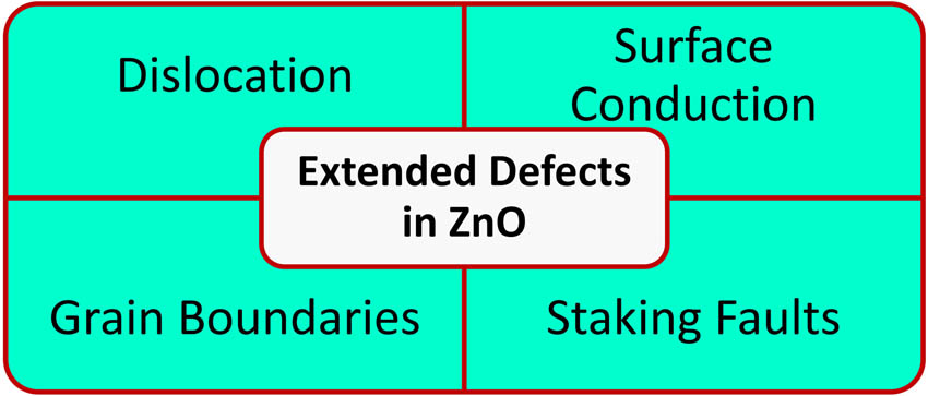
Different types of extended defects.
6.1 Surface conduction
The surface conduction layer of the ZnO samples possesses a free electron concentration of the order of (1–3) × 1012/cm2 [237,311]. Look et al. [311] studied the effect of the annealing and O2 plasma treatment on the bulk conductance and the surface conductance. They observed that only the surface conductance was affected by these treatments. The effect is clearly revealed in Figure 17. As the conduction band has small energy compared to vacuum, the Fermi level at the surface is most likely stuck over the conduction band smaller than the expected minimum [312]. This prompts a surface collection of electrons, like the circumstance in InN [313,314]. Uncovering the surface-to-air or O2 plasma lessens the conductivity of the layer, probably because of the adsorption of O2 and changes in the surface remaking [237,311]. Hall-effect estimations can be deciphered with a two-layer model, where the first layer is the surface leading channel and the subsequent layer is the hidden mass [315].
![Figure 17
Carrier concentration versus temperature for sample #2: (1) as-grown, (2) annealed at 715°C, (3) annealed at 700°C after irradiation, and (4) subjected to a remote O2 plasma. Reproduced with permission from Elsevier [311].](/document/doi/10.1515/ntrev-2022-0035/asset/graphic/j_ntrev-2022-0035_fig_017.jpg)
Carrier concentration versus temperature for sample #2: (1) as-grown, (2) annealed at 715°C, (3) annealed at 700°C after irradiation, and (4) subjected to a remote O2 plasma. Reproduced with permission from Elsevier [311].
6.2 Dislocation
Heteroepitaxial layers of ZnO ordinarily possess stringing disengagement densities of 109/cm2. Stringing dislocations, for the most part, runs along with the “c” pivot, even though ZnO developed under Zn-rich conditions gave a few dislocations 20–30° from the “c” axis [316]. Transmission electron holography reveals the presence of negative charges because of the aggregation of VZn’s close to the separation center [317]. The activation energy value for the separation movement was assessed to be of the order of 0.7–1.2 eV in the range 650–850°C [318]. Dislocations made by plastic disfigurement appear to expand the excitonic emission intensity [319]. ZnO has also been developed on r-cut sapphire as a single crystal; however, the interface contains a high thickness of nonconformist dislocations [320].
6.3 Stacking faults
Samples developed by molecular beam epitaxy on r-cut sapphire demonstrated a basal-plane stacking deficiency thickness of 105/cm and fractional disengagement density in the range of mid-1010/cm2 [321]. Calculations indicated that basal-plane stacking shortcomings have low development energies; however, they do not bring electronic states into the gap [322]. Nevertheless, spatially settled cathodoluminescence estimations demonstrated that basal-plane stacking deficiencies contain confined conditioning acceptors with a hole having a binding energy value of 130 meV [323]. The recombination of free electrons with acceptor-bound gaps prompts an outflow at 3.31 eV. An emanation at 3.333 eV was credited to excitons bound to structural imperfections [324].
6.4 Grain boundaries
Thin films faltered on “c”-cut sapphire displays columnar development, similar to GaN, with grain boundaries having small energy [325,326]. At the grain limits, a few molecules have triple or fivefold coordination. In ZnO developed on silica, a few sorts of [0001]-tilt grain limits has been identified [327]. Defects at grain limits assume a significant function in ZnO varistors and semiconductor gadgets fabricated of ceramics with profoundly nonlinear current-voltage attributes [328]. Varistors are protecting up to an all-around characterized breakdown field. They include conductive grains encompassed by added cations such as Bi or Pr, which isolate to the grain limit. Grain sizes are ordinarily around 10 μm with the common grain resistivity of the order of <1 Ω cm. A depletion region was observed to frame at each grain limit, where it lies completely inside the ZnO grain, as a result of which the breakdown voltage of ∼3 V/grain has been observed [329]. First-principle computations demonstrated that Bi may fill in for Zn molecules at the grain limit, bringing about a confined acceptor state [330]. This type of predicament leads to a creation of a p–n intersection between the grain limit and the n-type ZnO grain. Liang and shen. [331] studied the interfacial thermal and electrical transport characteristics of the grain boundaries in ZnO by studying the physical transport parameters of ZnO polycrystals with different grain boundary spacing [331]. They have studied the correlation between thermal conductivity and grain boundary under various environmental conditions. Studying the behavior under the temperature variation from the RT up to 1,073 K, they observed that the thermal conductivity first varies by changing the grain boundary spacing at RT but latterly shows independence on grain boundary spacing with the increase in temperature. For further understanding of the grain boundaries, the effect of electron concentration and mobility have also been considered.
7 General remarks about defects
To sum up what is thought about local defects, Vo’s prove to be profound contributors but unable to provide a proper explanation about the experimental n-type conductivity in ZnO. Nonetheless, they can remunerate p-type doping. Zni proves to be a shallow contributor, although it possesses large formation energies under n-type characteristics. In addition, it has been observed that it diffuses at a very fast rate and henceforth probably not going to be steady as confined point defects. Zna is similarly a shallow donor; however, it possesses large formation energies in n-type samples. Zna reveals the characteristic of massive off-site removal and instigates a huge neighborhood cross section unwinding. VZn’s are profound acceptors but possess very low formation energies under n-type conditions; they can hence happen as repaying surrenders in n-type samples. It is usually recommended that VZn’s are a probable source of the frequently observed green luminescence in ZnO. Oi have excessive formation energies and are not estimated to exist in substantial concentration. They are usually present in an electrically inert split interstitial or as profound acceptors at the octahedral site in n-type tests. Oa possess the most remarkable arrangement energies among the acceptor-type local point defects. Zni’s possess a diffusion mechanism with a fairly low relocation hindrance of 0.57 eV, concurrence with trial perceptions, and are liable for the watched quick recuperation of the electrical properties in illuminated ZnO. The relocation boundary of Oi in the octahedral arrangement is 1.1 eV, although VZn and Vo diffuse with relatively higher movement hindrances of 1.4 and 2.4 eV, individually.
8 Applications of ZnO
ZnO is one of the most widely used metal oxides with numerous applications due to its diverse characteristics and extensive activities in the industrial sector [116]. ZnO has applications in every aspect of life. It is being used in materials science, engineering, chemistry, and environmental science, etc. It possesses many applications in multiple areas such as in electrical and optical devices, sensors, cosmetic materials, solar cells, windows, drug delivery, LEDs, and lithium-ion batteries [332]. Besides the above-mentioned applications, it also has applications such as plastic and rubber fillers, photocatalytic antibacterial agent [333]. The above-mentioned applications of ZnO are categorized as shown in Figure 18. Among the mentioned categories, the applications in the textile industry analyzing the absorbing nature of ZnO for UV radiations. Second, a brief discussion will be provided on the pharmaceutical and cosmetic industry on the use of ZnO in medicine. Finally, the electrotechnology industry with the main focus on use of ZnO in sensors, solar cells, field emitter such as LED and supercapacitors will be discussed.
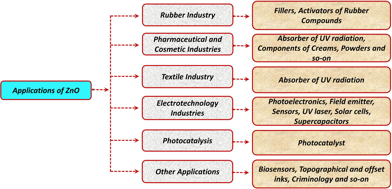
Schematic representation of applications of ZnO in different fields.
8.1 Textile industry
For the commercialization of nanotechnological products, the textile industry plays an important role. Especially, water repellent and self-cleaning textiles are important for the military purposes due to the lack of time for laundry in extreme circumstances. Not only for the military purpose, but the water repellent textiles possess a considerable demand in the world-class business also [4]. Mainly, the body’s resistance from the effect of the harmful UV radiation is the vital area of the research, where the researchers need to devote. A large number of scientists are working on the development of self-cleaning, water repellent, and UV-blocking textiles [334–339]. Sunlight is the primary source of UV radiation, which affects the human immune system and skin over time. To protect from the passive damage, the UV absorbers are frequently developed in the form of organic coatings. Nevertheless, the UV absorbers developed from the organic materials face the problem of stability due to migration and the degradation phenomenon. However, the UV absorbers developed from inorganic substances are found to be stable and do not face any degradation issues. When comparing textiles made with inorganic constituents for UV protection to those made with organic constituents, it has been discovered that the textiles made with inorganic constituents are far more stable.
They are also extensively used because of their tiny size. In this regard, the ZnO NPs are inexpensive for UV-blocking applications [340,341]. For the textile industry, ZnO nanostructures are very efficient because the nanostructured coatings are air-permeable with higher UV-blocking property compared to their counterparts [342]. Among the different kinds of available nanostructures, the coating of the ZnO proves to be an efficient UV-protective textile. So far, many techniques have been used for the fabrication of UV-protecting textiles, among which the hydrothermally grown ZnO NPs in SiO2-coated fabric show an efficient UV-blocking property [343]. Also, it has been observed that the synthesis of the ZnO NPs via homogeneous phase reaction followed by the deposition on the fabrics (cotton or wool) results in the enhancement of the UV-absorbing property [344]. Similarly, the ZnO NRs have shown excellent UV-protecting properties grown on a fibrous substrate via a low-temperature growth technique [345]. Ates and Unalan [346] utilized the microwave-assisted hydrothermal method for synthesizing the ZnO NWs on the cotton fabric to investigate the properties such as self-cleaning, super-hydrophobicity, and UV-protection. The super-hydrophobic nature was analyzed by functionalizing with the stearic acid for obtaining the water contact angle of 150° and was found to be stable. They also have studied the effect on the hydrophobicity of the cotton surface by utilizing the water contact angle measurements. The different studies they performed using the contact angle measurement technique are depicted in Figure 19.
![Figure 19
(a) Water contact angle measurement of surface-modified ZnO NW coated cotton fabric. (b) Digital picture of (i) bare, (ii) coated with ZnO seeds, (iii) coated with ZnO NWs, and (iv) cotton fabrics after methylene blue solution staining. Reproduced with permission from Elsevier [346].](/document/doi/10.1515/ntrev-2022-0035/asset/graphic/j_ntrev-2022-0035_fig_019.jpg)
(a) Water contact angle measurement of surface-modified ZnO NW coated cotton fabric. (b) Digital picture of (i) bare, (ii) coated with ZnO seeds, (iii) coated with ZnO NWs, and (iv) cotton fabrics after methylene blue solution staining. Reproduced with permission from Elsevier [346].
8.2 Pharmaceutical and cosmetic industries
ZnO has been widely used for different kinds of medicinal purposes because of its drying, antibacterial, and disinfecting properties [210,347]. Earlier, it was used for curing epilepsy and diarrhea, but now it is being used in ointments and creams along with its use for dusting and liquid powders. The efficient behavior of ZnO for wound healing makes it suitable for developing medicines in dermatology, especially for inflammation and itching purposes. It is also being used for suppositories, in dentistry for dental paste, and temporary fillings [4]. ZnO also finds its use in different dietary supplements and goods, providing dietary Zinc [348]. Before the evolution of the ZnO NPs, the sunscreen creams contained thick preparations that did not rub easily on the skin, resulted in rare cosmetics uses. The use of ZnO NPs in creams has solved the disadvantage mentioned above, enhancing the quality, and providing the propensity to absorb the UVA and UVB radiations. Adding the titanium dioxide (TiO2) to the ZnO for the fabrication of the cream provides an effective medium that possesses properties like highly transparency, less sticky, and being easily massaged into the skin [349]. A large number of reports have suggested that the combination of TiO2 and ZnO yields better results as it absorbs UV radiations, provides no irritation to the skin, and is easily absorbed into the skin [350–353].
8.3 Electrotechnological industries
ZnO is a significant semiconductor that possesses a diverse function in electrotechnology [354–356]. As mentioned earlier, ZnO is a wide band-gap metal oxide semiconductor and possesses high bond energy which makes it an efficient candidate for photoelectronic and electronic types of equipment [357,358]. Also, it finds its applications in the devices emitting surface acoustic waves [359], field emitters [360], sensors [361–366], UV lasers [367], and solar cells [368]. Because of the ZnO luminescence properties, it is being used in field emission displays. With the high electrical conductivity and good resistance against UV radiations, it replaces the conventional materials. Thin films made from the ZnO show high permeability and high conductivity and hence are being used to fabricate light-permeable electrodes in solar batteries. In photovoltaic cells and electroluminescent devices, it is being used as a transparent electrode and also acts as an encouraging candidate for UV-emitting devices [369,370]. Among a large number of properties in the electrotechnological devices, the important applications are discussed below:
8.3.1 Sensors
The high sensitivity to the chemical environment makes ZnO an efficient material for many sensing applications. The electronic processes are greatly influenced by surface phenomenon, and hence, preferential materials are readily chosen as nanostructures for their high surface area. The NWs fabricated from the ZnO show high sensitivity even at RT, whereas thin film gas sensors start functioning at elevated temperatures. The sensing process relies on the number of oxygen vacancies at the surface. The oxidation and the reduction processes lead to the decrease and increase in the conductivity, respectively. The main focus is the detection of certain gases. NR structured device fabricated from the ZnO has been developed and used to detect the H2 gas. The palladium (Pd) clusters were deposited on the ZnO rod surface by sputtering process to increase its sensing activity. The deposition of Pd increases the sensing as it dissociates the H2 into its atomic hydrogen, increasing the sensing activity. It has been observed that it shows the tendency to recover its conductance up to 95% within 20 s after exposing the sensor to the air [371]. H2 sensitivity by the platinum (Pt)-coated ZnO NRs have also been reported [372]. Rout et al. [373] utilized the thick film fabricated from the ZnO NPs for the H2 sensing. Also, a demonstration of the sensors from single NWs of ZnO with field-effect transistor geometry and O2, NO2, and NH3 as oxidizing agents was reported [374,375]. It has been observed that the small diametric NWs have a higher oxygen sensitivity and can be regulated by a gate voltage. Large negative gate voltage leads to the desorption of the NO2 molecules, so that can be used for the refreshment of the sensor. Observations show that using Pt-integrated electrodes in the sensors revealed better results. An ethanol sensor with Pt-integrations has shown better sensitivity and quick response at 300°C [376]. Xiangfeng et al. [377] demonstrated that the sensor response was strongly dependent on the fabrication atmosphere. They synthesized the ZnO tetrapod by evaporating pure ZnO in four different gas flows, that is, humidified argon (Ar), dry Ar, humidified N2, and dry N2. They observed that the sensor prepared in the humidified Ar flow reveals the fast response and a good selective behavior in detecting the ethanol. Ruthenium-sensitized ZnO gas sensor developed to detect oxygen and carbon monoxide at RT by utilizing the surface photocurrent. They observed that the sensing capability was highly influenced by the gas molecules that remain adsorbed on the surface [378]. With a growing demand for the development of sensors, glucose biosensor in the form of ZnO NRs has been synthesized by the hydrothermal decomposition method [379]. Currently, researchers mainly focus on how to harvest environmental energy. In this regard, the PNGs are the new burgeoning that offer a new track for harvesting the mechanical energies. These generators work on the principle that when nanometric scale piezoelectric material is deformed by some external source, piezoelectric potentials rise [380]. These PNGs, when connected to an external load, maintain the current in the circuit as long as the mechanical movement continues. The ZnO NR-based nanogenerators were first studied in 2006 where it was observed that mechanical deformation leads to the flow of electrons in the external load. Soon after this discovery, an enormous number of researchers have started working in this field, and a large number of ZnO NR-based piezoelectric devices have been fabricated such as piezoelectric gate diodes [381], field-effect transistors [382,383], pressure-based sensors [384,385], biomedical sensors [386,387], and PNGs [388,389]. These PNGs found applications in energy harvesting [176,390–393], self-powering motion sensors [394], pressing sensors [395], and piezo-biosensors [386]. Cue et al., in 2016 [396], have synthesized different structures of the ZnO by utilizing the electrospinning and the hydrothermal route to study the effect of the morphology of the ZnO on the activity of the HCHO gas sensor. They found that the HCHO gas sensor has a greater sensitive response and a faster recovery time for different irradiation sources than other sensors. They also studied the influence of the nanostructure shape on the working mechanism. The outlay of the sensing mechanism is shown in Figure 20. The studies revealed that because of the tiny grain size, the developed nanofibers have the strongest sensing responsivity because of the observed significant change in the depletion region (Figure 20(a)). In comparison to these, the NPs that possess the bigger particle size cause slight shifting of the depletion region by signifying the nanofibers weaker sensing response (Figure 20(b)).
![Figure 20
Gas sensing mechanism of ZnO nanofibers under UV illumination: (a) ZnO nanoplates and (b) ZnO nanoflowers in the presence of HCHO. Reproduced with permission from Elsevier [396].](/document/doi/10.1515/ntrev-2022-0035/asset/graphic/j_ntrev-2022-0035_fig_020.jpg)
Gas sensing mechanism of ZnO nanofibers under UV illumination: (a) ZnO nanoplates and (b) ZnO nanoflowers in the presence of HCHO. Reproduced with permission from Elsevier [396].
Sett and Basak [397] studied the sensing ability of the cobalt-doped ZnO for the H2 gas. They investigated the effect of the different parameters such as temperature and doping on the sensing ability. While studying the effect of the concentration on the sensing response, they found that an 8% doping level of the cobalt in the ZnO shows the highest sensing response as is clearly indicated in Figure 21(a) and (b). The enhanced sensing response has been attributed to the high surface-to-volume ratio of the NRs, resulting to the enhancement in the oxygen vacancies (Figure 21(c)). Chen et al. [398] fabricated the zinc NWs by utilizing hydrothermal methods. They studied the effect of the functionalization with Pd/PdO on the sensing ability of nitrogen dioxide. While studying the gas sensing behavior, they observed a change in the resistance by changing the NO2 concentration. The sensing ability of ZnO has been proved to be efficient for different sensors. Besides enhancing the properties and characteristics of the available ZnO-based sensors, researchers are working on further developments. They are devoting time to bring a new version of the sensors, which the community requires.
![Figure 21
(a) Gas response with different Co-doping contents at 300°C, (b) gas response of all sensors for different H2 concentration at 300°C, and (c) sensing mechanism of undoped and Co-doped ZnO NRs. Reproduced with permission from Elsevier [397].](/document/doi/10.1515/ntrev-2022-0035/asset/graphic/j_ntrev-2022-0035_fig_021.jpg)
(a) Gas response with different Co-doping contents at 300°C, (b) gas response of all sensors for different H2 concentration at 300°C, and (c) sensing mechanism of undoped and Co-doped ZnO NRs. Reproduced with permission from Elsevier [397].
8.3.2 LEDs
From the very beginning, the ZnO has been used for the development of the conventional blue LEDs by using different types of substrates such as sapphire [399,400], GaN [401], and SiC [402]. LEDs development with ZnO on these substrates has been studied to a great extent, both theoretically and experimentally. Bulashevich et al. [403,404] studied the operation of the ZnO/GaN-based heterostructure diodes by simulation. They discussed the mechanism of working of such heterostructures diodes and laser diodes. Also, they studied internal parameters such as internal quantum efficiency and its temperature dependence. Kozuka et al. [405] came up with an elaborated review on ZnO/MgZnO heterostructures for LEDs and other optical applications. The article covers the large areas of heterostructure LEDs ranging from growth techniques, band alignment to device fabrication, and discussions on characterization. It has been observed that it is quite simple to develop the epitaxial heterostructures LED structure containing ZnO because of their lattice mismatch than III–IV homogeneous LEDs [406]. This simplicity is provided only by the ionic nature of ZnO, as ionic bonds possess spherical potential wells compared to the anisotropy found in covalently bonded semiconductors. It is worth mentioning that ZnO proves itself to be a promising candidate for a light generation with its crystallites so small in size that they show quantum confinements and hence described as ZnO quantum dots (QDs) [407]. Mikrajuddin et al. [408] and Zhong et al. [409] developed the LEDs based on ZnO QDs by using different synthetic routes. For enhancing the applicability of the ZnO QDs, Liang et al. [410] synthesized the ZnO QD-phosphors nanocomposites by sol–gel methods. The synthesized nanocomposite consists of yellow-emitting ZnO QDs and a europium-doped blue-emitting phosphor, both were interlinked by the use of silica. Besides achieving the white light for the QD nanocomposite, the PL quantum yield and the luminous efficiencies were calculated and found to be 63.7% and 73.6 lm/W, respectively [410]. The ZnO has attracted attention in this field because of its simple synthetic procedure and tuneability of the fluorescence. The life span of ZnO QDs is the factor restricting their far-reaching use right now. When legitimate embodiment strategies are created to delay their usable lifetime, this material will probably arise as a genuine competitor for making both UV and green-emitting LEDs. Another purpose behind the ubiquity of ZnO QDs is that they can be utilized both as an intrinsic light-emitting layer when integrated inside the structure of LEDs, and as an external phosphor when covered on top of blue or UV LEDs [407]. The researchers also have studied the effect of the rare earth doping on the PL properties of the ZnO, and the research in this regard is going on for the further developments. Kumar et al. [411] studied the effect of the terbium-doped ZnO and find it suitable for the solid-state lighting technology. Besides studying the PL emission, they also investigated the different transitions responsible for the emission. They also found the Commission International de l eclairage (CIE) coordinates of the synthesized compound as shown in Figure 22(a–d). They further concluded that the visible emission shown by the ZnO arises only because of the different defects, that is, oxygen vacancy and the Oi. The remarkable properties shown by the ZnO for the lighting technology have forced the researchers to explore the properties. In this regard, the researchers have used different synthesis methods and different rear-earth (RE) dopants as depicted in the CIE diagram Figure 22(e).
![Figure 22
(a) PL emission with different Tb3+ concentration, (b) logarithmic plot of I/C as a function of the activator concentration, (c) schematic energy level diagram, and (d) CIE diagram of ZnO:Tb3+ nanophosphors. Reproduced with permission from Elsevier [411]. (e) CIE diagram of undoped and RE-doped ZnO NPrs with different synthesis conditions. Reproduced with permission from Elsevier [6].](/document/doi/10.1515/ntrev-2022-0035/asset/graphic/j_ntrev-2022-0035_fig_022.jpg)
(a) PL emission with different Tb3+ concentration, (b) logarithmic plot of I/C as a function of the activator concentration, (c) schematic energy level diagram, and (d) CIE diagram of ZnO:Tb3+ nanophosphors. Reproduced with permission from Elsevier [411]. (e) CIE diagram of undoped and RE-doped ZnO NPrs with different synthesis conditions. Reproduced with permission from Elsevier [6].
8.3.3 Solar cells
In the past few years, ZnO has been used to fabricate electrode materials for dye-sensitized solar cells [412–414]. It has been observed that the transfer of electrons from the dye to the conduction band of ZnO happens in a very short interval of time compared to the previously used TiO2 layers [415–418]. Among a large number of available nanostructures, ZnO acts as an efficient candidate because of its wide bandgap, high charge carrier mobility, and also high surface area, which are necessary for dye-sensitization and light-harvesting devices. The filling of the pores of these nanoporous structures remains the main challenging work for these solar cells as only a few materials can fill the nanopores of TiO2 layers [419,420]. Various researchers have also synthesized hybrid structures of the dye-sensitized solar cells with different synthetic routes. In this regard, Weintraub et al. [421] synthesized the hybrid 3-D NW for the dye-sensitized solar cells, as shown in Figure 23(a) and (b). The NWs of the ZnO have been developed parallel to the optical fiber in such a way that light will lit the fiber axially from one end. As the light enters the fiber, the phenomenon of the internal reflection enables the light to interact with the dye-sensitized molecules. Due to this continuous interaction, researchers observed an increment upto 3.3% in the sun efficiency, almost 120% greater than the previous high figures. The particular electrode shapes that have been used in the fiber led to the many restrictions in the functionality of these hybrid structures. For resolving the issue, the same group came up with a new version of the hybrid structure in which the optical fiber has been replaced by the quartz slide as shown in Figure 23(c) and (d) [422]. In the new design, the 3-D dye-sensitized solar cells have been developed by interposing the ZnO NW on the quartz slides with planar electrodes. The developed solar cell functions as a wave-guide for the transmission of light. The fabricated device led to an increment in the energy conversion efficiency up to 5.8% as compared to the previous one [422]. Gonzalez-valls et al. [423] synthesized vertically aligned ZnO NRs and used them as electrodes in dye-sensitized solar cells. They studied the changing effect of various parameters such as light intensity, temperature, and UV-light on the final photovoltaic properties. As a result, they found that the increase in the light intensity and temperature affects the series and shunt resistances and finally led to the decrease in the solar cell efficiency. Synthesizing the ZnO-branched NRs by the hierarchical solution method can be used for the applications such as solar cells, UV-lasers, and sensors [424].
![Figure 23
Design and principle of a 3-D dye-sensitized solar cells (DSSC). The cross section of the fiber can be cylindrical or rectangular. (a) The 3-D DSSC is composed of optical fibers and ZnO NWs are grown vertically on the fiber surface. The top segment of the bundled optical fibers utilizes conventional optical fibers and allows for remote transmission of light. The bottom segment consists of the 3-D DSSC for solar power generation at a remote/concealed location. (b) Detailed structure of the 3-D DSSC. Reproduced with permission from Wiley-VCH [421]. (c) Schematic architecture of a large-scale 3-D DSSC. The waveguide-NW 3-D unit SCs are plugged into the counter electrode housing and then sealed and fully packaged. (d) Detailed structure of a unit waveguide-NW 3-D DSSC. Reproduced with permission from American Chemical Society [422].](/document/doi/10.1515/ntrev-2022-0035/asset/graphic/j_ntrev-2022-0035_fig_023.jpg)
Design and principle of a 3-D dye-sensitized solar cells (DSSC). The cross section of the fiber can be cylindrical or rectangular. (a) The 3-D DSSC is composed of optical fibers and ZnO NWs are grown vertically on the fiber surface. The top segment of the bundled optical fibers utilizes conventional optical fibers and allows for remote transmission of light. The bottom segment consists of the 3-D DSSC for solar power generation at a remote/concealed location. (b) Detailed structure of the 3-D DSSC. Reproduced with permission from Wiley-VCH [421]. (c) Schematic architecture of a large-scale 3-D DSSC. The waveguide-NW 3-D unit SCs are plugged into the counter electrode housing and then sealed and fully packaged. (d) Detailed structure of a unit waveguide-NW 3-D DSSC. Reproduced with permission from American Chemical Society [422].
8.3.4 Supercapacitors
In the current scenario of the growing technological world, the storage of energy in different forms is crucial by the research community. Among the different energy storage devices, batteries and capacitors are considered to be the most prominent. But, due to the fact that batteries were being used for the systems that require high energy density at low output power and capacitors were being used for the systems that require high output power, limits their utility for the systems, which require high energy and power density. For solving the inadequacy, the different devices, such as electrochemical capacitors, supercapacitors, and ultracapacitors, have been analyzed for meeting the demands. Among the mentioned devices, the supercapacitors proved to be very efficient and became the effective solution for the rising energy demands, which is a growing challenge in today’s world [425]. These supercapacitors have been categorized into many types, such as electrochemical double-layered capacitors, hybrid capacitors, and pseudocapacitors, depending on their design geometry [425,426]. ZnO has played an important role in these energy storage devices by acting as an electrode in the devices [427,428]. Li et al. [429] have used the hydrothermal method and prepared zinc-cobalt oxide and sulfide hydride. By comparing their fabricated materials with zinc-cobalt binary oxide nanosheets, they observed that the substitution of oxygen by sulfur results in the generation of a more flexible structure along with the development of efficient and rapid pathways for ion and electron transport. These properties became evident by the exceptional cyclic stability and very high specific capacitance of the materials of 2176.7 F/g at 1 A/g, which is nearly six times higher than the zinc-cobalt binary oxide nanosheets of 367.2 F/g at 1 A/g [429]. Pant et al. [430] fabricated the ZnO nanoflakes wrapped carbon nanofiber composites for utilizing them as electrode materials in the supercapacitors. They fabricated these composites by combining the electrospinning technology with the hydrothermal process. It has been reported that the composite formed possesses a diameter of the order of 300 nm along with the length of hundreds of micrometers, which provides high aspects. The specific capacitance of the composite has been found to be 260 F/g. From the obtained results, it has been calculated that such types of composites are suitable electrode materials for supercapacitors. Many other researchers have also analyzed the capability of the ZnO as an electrode for the supercapacitors. They have observed that ZnO proves to be an efficient electrode material for the supercapacitors [431–433]. It is all due to the remarkable properties of the ZnO, that is, broad bandgap, presence of a large number of defects, high electron mobility, etc., which make it a promising material for supercapacitors. With the growing technological advancements in each and every corner of science and technology, the researchers will be able to develop next-generation high-power capacitors in the coming years, which will definitely serve as an alternative for energy storage devices.
9 Conclusion and future perspective
In spite of a large number of difficulties in achieving the p-type conductivity, both intrinsic and defect-related properties of ZnO have significant advantages for device applications. From the above study, it is clear that significant efforts have been devoted both experimentally and theoretically to understand the nature and role of these defects. Predominant imperfection species and their significance to the electrical and optical properties are discussed based on determined formation energies, donors and acceptor levels, optical transition energies, and electronic structures of the deformities. The oxygen vacancy acts as an efficient donor type-defect and possesses the lowest formation energy among the native defects. In comparison to the oxygen, the VZn’s have sufficiently high formation energies and act as an acceptor type native defect with low hole concentrations. The interstitials and the antisites of the oxygen have high formation energy with neutral behavior concerning electrical activity. Because of the neutral electrical response, they do not play any significant role in the electrical properties under equilibrium conditions. The interstitials and the antisites of the zinc possess the high formation energies in the n-type ZnO and act as shallow donors. This review provides a brief idea regarding the defects in ZnO, as this topic is the hotbed for many areas of science and technology. With the growing research in this field, more and more knowledge will be obtained, which will ultimately lead to stronger evidence for many new phenomena. In this bibliographic review, we tried to show ZnO NPs have exceptionally unique properties that are all the outcomes of the defects. All of these aspects combine to make this nanomaterial a very adaptable system, which is used both individually and the combination of the other materials. This aspect demonstrates that the ZnO NPs can be used in almost any sector of science and technology. Regardless of lot of applications of ZnO in the various sectors of the science and technology, there is still a requirement of growth along with the right knowledge of the numerous phenomena, which includes biological effects of the ZnO, effect of the core-shell design on the different properties etc. In addition, these consistency in the reproducibility of the ZnO NPs remains a project for the researchers. Concerning application, a lot of work still needs to be done for the proper upgradation of the different applications such as theranostic, criminology, fingerprinting, and food packaging. Finally, science and technology of nano and micrometric oxides are now the day’s most rapidly evolving scientific and technical specialties. Working on ZnO, in this regard, can also help in the fabrication of more durable ceramics, transparent solar screens that can resist infrared and UV light, etc. Most importantly, the usage of the ZnO for therapy and drug delivery is still an open arena for the research community, which needs a lot of attention.
-
Funding information: SDU authors acknowledge the funding by Interreg Deutschland–Denmark with money from the European Regional Development Fund, project number 096-1.1-18 (Access and Acceleration).
-
Author contributions: All authors have accepted responsibility for the entire content of this manuscript and approved its submission.
-
Conflict of interest: The authors state no conflict of interest.
References
[1] Schönnenbeck M. History of Zinc, its production and usage. Bericht Reports; 2013.Search in Google Scholar
[2] Segets D, Gradl J, Taylor RK, Vassilev V, Peukert W. Analysis of optical absorbance spectra for the determination of ZnO nanoparticle size distribution, solubility, and surface energy. ACS Nano. 2009;3:1703–10. 10.1021/nn900223b.Search in Google Scholar PubMed
[3] Lou X, Shen HS, Shen YS. Development of ZnO series ceramic semiconductor gas sensors. J Sens Trans Technol. 1991;3:1–5.Search in Google Scholar
[4] Kolodziejczak-Radzimska A, Jesionowski T. Zinc oxide-from synthesis to application: A review. Materials. 2014;7:2833–81. 10.3390/ma7042833.Search in Google Scholar PubMed PubMed Central
[5] Dutta S, Chattopadhyay S, Sarkar A, Chakrabarti M, Sanyal D, Jana D. Role of defects in tailoring structural, electrical and optical properties of ZnO. Prog Mater Sci. 2009;54:89–136. 10.1016/j.pmatsci.2008.07.002.Search in Google Scholar
[6] Kumar V, Ntwaeaborwa OM, Soga T, Dutta V, Swart HC. Rare earth doped zinc oxide nanophosphor powder: A future material for solid state lighting and solar cells. ACS Photonics. 2017;4:2613–37. 10.1021/acsphotonics.7b00777.Search in Google Scholar
[7] Janotti A, Van de Walle CG. Fundamentals of zinc oxide as a semiconductor. Rep Prog Phys. 2009;72:126501. 10.1088/0034-4885/72/12/126501.Search in Google Scholar
[8] McCluskey MD, Jokela SJ. Defects in ZnO. J Appl Phys. 2009;106:071101. 10.1063/1.3216464.Search in Google Scholar
[9] Pearton SJ, Norton DP, Ip K, Heo YW, Steiner T. Recent advances in processing of ZnO. J Vac Sci Technol B Microelectron Nanom Struct. 2004;22:932. 10.1116/1.1714985.Search in Google Scholar
[10] Look DC. Progress in ZnO materials and devices. J Electron Mater. 2006;35:1299–305. 10.1007/s11664-006-0258-y.Search in Google Scholar
[11] Mishra YK, Modi G, Cretu V, Postica V, Lupan O, Reimer T, et al. Direct growth of freestanding ZnO tetrapod networks for multifunctional applications in photocatalysis, UV photodetection, and gas sensing. ACS Appl Mater Interfaces. 2015;7:14303–16. 10.1021/ACSAMI.5B02816.Search in Google Scholar PubMed
[12] Özgür Ü, Alivov YI, Liu C, Teke A, Reshchikov M, Doğan S, et al. A comprehensive review of ZnO materials and devices. J. Appl. Phys. 2005;98:041301. 10.1063/1.1992666. Search in Google Scholar
[13] Rana HS, Shaikh SF, Al-Enizi AM, Agyeman DA, Ghani F, Nah IW, et al. Intrinsic control in defects density for improved ZnO nanorod-based UV sensor performance. Nanomaterials. 2020;10:142. A.10.3390/nano10010142.Search in Google Scholar
[14] Auret FD, Meyer WE, Janse van Rensburg PJ, Hayes M, Nel JM, von Wenckstern H, et al. Electronic properties of defects in pulsed-laser deposition grown ZnO with levels at 300 and 370 meV below the conduction band. Phys B Condens Matter. 2007;401–402:378–81. 10.1016/j.physb.2007.08.192.Search in Google Scholar
[15] Cantwell G, Harsch WC, Jogai B. Valence-band ordering in zno. Phys Rev B – Condens Matter Mater Phys. 1999;60:2340–4. 10.1103/PhysRevB.60.2340.Search in Google Scholar
[16] Reynolds DC, Look DC, Jogai B. Optically pumped ultraviolet lasing from ZnO. Solid State Commun. 1996;99:873–5. 10.1016/0038-1098(96)00340-7.Search in Google Scholar
[17] Bagnall DM, Chen YF, Zhu Z, Yao T, Koyama S, Shen MY, et al. Optically pumped lasing of ZnO at room temperature. Appl Phys Lett. 1997;70:2230–2. 10.1063/1.118824.Search in Google Scholar
[18] Mishra YK, Adelung R. ZnO tetrapod materials for functional applications. Mater Today. 2018;21:631–51. 10.1016/J.MATTOD.2017.11.003.Search in Google Scholar
[19] Klingshirn C. ZnO: From basics towards applications. Phys Status Solidi Basic Res. 2007;244:3027–73. 10.1002/pssb.200743072.Search in Google Scholar
[20] González-Garnica M, Galdámez-Martínez A, Malagón F, Ramos CD, Santana G, Abolhassani R, et al. One dimensional Au-ZnO hybrid nanostructures based CO2 detection: Growth mechanism and role of the seed layer on sensing performance. Sens Actuators B Chem. 2021;337:129765. 10.1016/J.SNB.2021.129765.Search in Google Scholar
[21] Brillson L, Cox J, Gao H, Foster G, Ruane W, Jarjour A, et al. Native point defect measurement and manipulation in ZnO nanostructures. Materials. 2019;12:2242. 10.3390/ma12142242.Search in Google Scholar PubMed PubMed Central
[22] Le AT, Ahmadipour M, Pung SY. A review on ZnO-based piezoelectric nanogenerators: Synthesis, characterization techniques, performance enhancement and applications. J Alloy Compd. 2020;844:156172. 10.1016/j.jallcom.2020.156172.Search in Google Scholar
[23] Look DC. Recent advances in ZnO materials and devices. Mater Sci Eng B. 2001;80:383–7. 10.1016/S0921-5107(00)00604-8.Search in Google Scholar
[24] Fabian J, Žutić I, Sarma SD. Spin injection through the depletion layer: A theory of spin-polarized p-n junctions and solar cells. Phys Rev B. 2001;64:121201. 10.1103/PhysRevB.64.121201.Search in Google Scholar
[25] Kikkawa JM, Awschalom DD. Lateral drag of spin coherence in gallium arsenide. Nature. 1999;397:139–41. 10.1038/16420.Search in Google Scholar
[26] Didosyan YS, Hauser H, Reider GA, Toriser W. Fast latching type optical switch. J Appl Phys. 2004;95:7339–41. 10.1063/1.1669350.Search in Google Scholar
[27] Rana AHS, Chang S-B, Kim H-S. NH4OH-Oriented and pH-dependent growth of ZnO nanostructures via microwave-assisted growth method. J Nanosci Nanotechnol. 2017;18:2125–7. 10.1166/jnn.2018.14961.Search in Google Scholar PubMed
[28] Somvanshi D, Jit S. Analysis of temperature-dependent electrical characteristics of n-ZnO nanowires (NWs)/p-Si heterojunction diodes. IEEE Trans Nanotechnol. 2014;13:62–9. 10.1109/TNANO.2013.2290553.Search in Google Scholar
[29] Rana AHS, Kang M, Jeong ES, Kim HS. Transition between ZnO nanorods and ZnO nanotubes with their antithetical properties. J Nanosci Nanotechnol. 2016;16:10772–6. 10.1166/jnn.2016.13237.Search in Google Scholar
[30] Vinod R, Sajan P, Achary SR, Tomas CM, Muñoz-Sanjosé V, Bushiri MJ. Enhanced UV emission from ZnO nanoflowers synthesized by the hydrothermal process. J Phys D: Appl Phys. 2012;45:425103. 10.1088/0022-3727/45/42/425103.Search in Google Scholar
[31] Rana AU, Shahid A, Lee JY, Kim HS. High-power microwave-assisted Ga doping, an effective method to tailor n-ZnO/p-Si heterostructure optoelectronic characteristics. Phys Status Solidi A. 2018;215:1700763. 10.1002/pssa.201700763.Search in Google Scholar
[32] Il Park W, Yi GC, Kim M, Pennycook SJ. ZnO nanoneedles grown vertically on Si substrates by non-catalytic vapor-phase epitaxy. Adv Mater. 2002;14:1841–3. 10.1002/adma.200290015.Search in Google Scholar
[33] Sun Y, Fuge GM, Ashfold MNR. Growth of aligned ZnO nanorod arrays by catalyst-free pulsed laser deposition methods. Chem Phys Lett. 2004;396:21–6. 10.1016/j.cplett.2004.07.110.Search in Google Scholar
[34] Yao BD, Chan YF, Wang N. Formation of ZnO nanostructures by a simple way of thermal evaporation. Appl Phys Lett. 2002;81:757–9. 10.1063/1.1495878.Search in Google Scholar
[35] Ul Hassan Sarwar Rana A, Ko K, Hong S, Kang M, Kim HS. Fabrication and characterization of ZnO nanorods on multiple substrates. J Nanosci Nanotechnol. 2015;15:8375–80. 10.1166/jnn.2015.11461.Search in Google Scholar
[36] Ul Hassan Sarwar Rana A, Kang M, Kim HS. Microwave-assisted facile and ultrafast growth of ZnO nanostructures and proposition of alternative microwave-assisted methods to address growth stoppage. Sci Rep. 2016;6:24870. 10.1038/srep24870.Search in Google Scholar
[37] Look DC, Reynolds DC, Sizelove JR, Jones RL, Litton CW, Cantwell G, et al. Electrical properties of bulk ZnO. Solid State Commun. 1998;105:399–401. 10.1016/S0038-1098(97)10145-4.Search in Google Scholar
[38] Sundaresan A, Bhargavi R, Rangarajan N, Siddesh U, Rao CNR. Ferromagnetism as a universal feature of nanoparticles of the otherwise nonmagnetic oxides. Phys Rev B. 2006;74:161306. 10.1103/PhysRevB.74.161306.Search in Google Scholar
[39] Thareja RK, Mitra A. Random laser action in ZnO. Appl Phys B Lasers Opt. 2000;71:181–4. 10.1007/s003400000274.Search in Google Scholar
[40] Li HD, Yu SF, Lau SP, Leong ESP. Simultaneous formation of visible and ultraviolet random lasings in ZnO films. Appl Phys Lett. 2006;89:021110. 10.1063/1.2221406.Search in Google Scholar
[41] Ong HC, Dai JY, Li ASK, Du GT, Chang RPH, Ho ST. Effect of a microstructure on the formation of self-assembled laser cavities in polycrystalline ZnO. J Appl Phys. 2001;90:1663–5. 10.1063/1.1374452.Search in Google Scholar
[42] Zu P, Tang ZK, Wong GKL, Kawasaki M, Ohtomo A, Koinuma H, et al. Ultraviolet spontaneous and stimulated emissions from ZnO microcrystallite thin films at room temperature. Solid State Commun. 1997;103:459–63. 10.1016/S0038-1098(97)00216-0.Search in Google Scholar
[43] Jiang JZ, Olsen JS, Gerward L, Frost D, Rubie D, Peyronneau J. Structural stability in nanocrystalline ZnO. Europhys Lett. 2000;50:48–53. 10.1209/epl/i2000-00233-9.Search in Google Scholar
[44] Xu Q, Schmidt H, Zhou S, Potzger K, Helm M, Hochmuth H, et al. Room temperature ferromagnetism in ZnO films due to defects. Appl Phys Lett. 2008;92:082508. 10.1063/1.2885730.Search in Google Scholar
[45] Lee WJ, Kang J, Chang KJ. Defect properties and p-type doping efficiency in phosphorus-doped ZnO. Phys Rev B. 2006;73:024117. 10.1103/PhysRevB.73.024117.Search in Google Scholar
[46] Guo L, Yang S, Yang C, Yu P, Wang J, Ge W, et al. Synthesis and characterization of poly(vinylpyrrolidone)-modified zinc oxide nanoparticles. Chem Mater. 2000;12:2268–74. 10.1021/cm9907817.Search in Google Scholar
[47] Uekawa N, Mochizuki N, Kajiwara J, Mori F, Wu YJ, Kakegawa K. Nonstoichiometric properties of zinc oxide nanoparticles prepared by decomposition of zinc peroxide. Phys Chem Chem Phys. 2003;5:929–34. 10.1039/b210990e.Search in Google Scholar
[48] Wang YS, Thomas PJ, O’Brien P. Nanocrystalline ZnO with ultraviolet luminescence. J Phys Chem B. 2006;110:4099–104. 10.1021/jp0566313.Search in Google Scholar PubMed
[49] Meulenkamp EA. Size dependence of the dissolution of ZnO nanoparticles. J Phys Chem B. 1998;102:7764–9. 10.1021/jp982305u.Search in Google Scholar
[50] Bredol M, Althues H. Luminescent Nano-sized ZnS and ZnO particles. Solid State Phenom 99–. 2004;100:19–24. 10.4028/www.scientific.net/SSP.99-100.19.Search in Google Scholar
[51] Dutta S, Chattopadhyay S, Sutradhar M, Sarkar A, Chakrabarti M, Sanyal D, et al. Defects and the optical absorption in nanocrystalline ZnO. J Phys Condens Matter. 2007;19:236218. 10.1088/0953-8984/19/23/236218.Search in Google Scholar
[52] Sharma P, Gupta A, Rao KV, Owens FJ, Sharma R, Ahuja R, et al. Ferromagnetism above room temperature in bulk and transparent thin films of Mn-doped ZnO. Nat Mater. 2003;2:673–7. 10.1038/nmat984.Search in Google Scholar PubMed
[53] Rubi D, Fontcuberta J, Calleja A, Aragonès L, Capdevila XG, Segarra M. Reversible ferromagnetic switching in ZnO:(Co, Mn) powders. Phys Rev B. 2007;75:155322. 10.1103/PhysRevB.75.155322.Search in Google Scholar
[54] Fujiwara H, Sasaki K. Observation of optical bistability in a ZnO powder random medium. Appl Phys Lett. 2006;89:071115. 10.1063/1.2338533.Search in Google Scholar
[55] Van De Walle CG. Hydrogen as a cause of doping in zinc oxide. Phys Rev Lett. 2000;85:1012–5. 10.1103/PhysRevLett.85.1012.Search in Google Scholar PubMed
[56] Smazna D, Rodrigues J, Shree S, Postica V, Neubüser G, Martins AF, et al. Buckminsterfullerene hybridized zinc oxide tetrapods: defects and charge transfer induced optical and electrical response. Nanoscale. 2018;10:10050–62. 10.1039/C8NR01504J.Search in Google Scholar
[57] Janotti A, Van De Walle CG. Oxygen vacancies in ZnO. Appl Phys Lett. 2005;87:122102. 10.1063/1.2053360.Search in Google Scholar
[58] Janotti A, Van de Walle CG. New insights into the role of native point defects in ZnO. J Cryst Growth. 2006;287:58–65. 10.1016/j.jcrysgro.2005.10.043.Search in Google Scholar
[59] Oba F, Togo A, Tanaka I, Paier J, Kresse G. Defect energetics in ZnO: A hybrid Hartree-Fock density functional study. Phys Rev B. 2008;77:245202. 10.1103/PhysRevB.77.245202.Search in Google Scholar
[60] Cabral L, Lopez-Richard V, Da Silva JLF, Marques GE, Lima MP, Onofre YJ, et al. Insights into the nature of optically active defects of ZnO. J Lumin. 2020;227:117536. 10.1016/j.jlumin.2020.117536.Search in Google Scholar
[61] Banerjee D, Lao JY, Wang DZ, Huang JY, Ren ZF, Steeves D, et al. Large-quantity free-standing ZnO nanowires. Appl Phys Lett. 2003;83:2061–3. 10.1063/1.1609036.Search in Google Scholar
[62] Hahn Y-B. Zinc oxide nanostructures and their applications. Korean J Chem Eng. 2011;28:1797–1813. 10.1007/s11814-011-0213-3.Search in Google Scholar
[63] Frade T, Melo Jorge ME, Gomes A. One-dimensional ZnO nanostructured films: Effect of oxide nanoparticles. Mater Lett. 2012;82:13–5. 10.1016/j.matlet.2012.05.028.Search in Google Scholar
[64] Wahab R, Ansari SG, Kim YS, Seo HK, Shin HS. Room temperature synthesis of needle-shaped ZnO nanorods via sonochemical method. Appl Surf Sci. 2007;253:7622–6. 10.1016/j.apsusc.2007.03.060.Search in Google Scholar
[65] Kong XY, Ding Y, Yang R, Wang ZL. Single-crystal nanorings formed by epitaxial self-coiling of polar nanobelts. Science. 2004;303:1348–51. 10.1126/science.1092356.Search in Google Scholar PubMed
[66] Pan ZW, Dai ZR, Wang ZL. Nanobelts of semiconducting oxides. Science. 2001;291:1947–9. 10.1126/science.1058120.Search in Google Scholar PubMed
[67] Wu JJ, Liu SC, Wu CT, Chen KH, Chen LC. Heterostructures of ZnO-Zn coaxial nanocables and ZnO nanotubes. Appl Phys Lett. 2002;81:1312–4. 10.1063/1.1499512.Search in Google Scholar
[68] Chen WJ, Liu WL, Hsieh SH, Tsai TK. Preparation of nanosized ZnO using α brass. Appl Surf Sci. 2007;253:6749–53. 10.1016/j.apsusc.2007.01.091.Search in Google Scholar
[69] Liu J, Huang X, Duan J, Ai H, Tu P. A low-temperature synthesis of multiwhisker-based zinc oxide micron crystals. Mater Lett. 2005;59:3710–4. 10.1016/j.matlet.2005.06.043.Search in Google Scholar
[70] Huang Y, He J, Zhang Y, Dai Y, Gu Y, Wang S, et al. Morphology, structures and properties of ZnO nanobelts fabricated by Zn-powder evaporation without catalyst at lower temperature. J Mater Sci. 2006;41:3057–62. 10.1007/s10853-006-6978-9.Search in Google Scholar
[71] Nikoobakht B, Wang X, Herzing A, Shi J. Scalable synthesis and device integration of self-registered one-dimensional zinc oxide nanostructures and related materials. Chem Soc Rev. 2013;42:342–65. 10.1039/c2cs35164a.Search in Google Scholar PubMed
[72] Tien LC, Pearton SJ, Norton DP, Ren F. Synthesis and microstructure of vertically aligned ZnO nanowires grown by high-pressure-assisted pulsed-laser deposition. J Mater Sci. 2008;43:6925–32. 10.1007/s10853-008-2988-0.Search in Google Scholar
[73] Cui J. Zinc oxide nanowires. Mater Charact. 2012;64:43–52. 10.1016/j.matchar.2011.11.017.Search in Google Scholar
[74] Xu T, Ji P, He M, Li J. Growth and structure of pure ZnO micro/nanocombs. J Nanomater. 2012;2012:797935. 10.1155/2012/797935.Search in Google Scholar
[75] Chiu WS, Khiew PS, Cloke M, Isa D, Tan TK, Radiman S, et al. Photocatalytic study of two-dimensional ZnO nanopellets in the decomposition of methylene blue. Chem Eng J. 2010;158:345–52. 10.1016/j.cej.2010.01.052.Search in Google Scholar
[76] José-Yacamán M, Gutierrez-Wing C, Miki M, Yang DQ, Piyakis KN, Sacher E. Surface diffusion and coalescence of mobile metal nanoparticles. J Phys Chem B. 2005;109:9703–11. 10.1021/jp0509459.Search in Google Scholar
[77] Polshettiwar V, Baruwati B, Varma RS. Self-assembly of metal oxides into three-dimensional nanostructures: synthesis and application in catalysis. ACS Nano. 2009;3:728–36. 10.1021/nn800903p.Search in Google Scholar
[78] Xie Q, Dai Z, Liang J, Xu L, Yu W, Qian Y. Synthesis of ZnO three-dimensional architectures and their optical properties. Solid State Commun. 2005;136:304–7. 10.1016/j.ssc.2005.07.023.Search in Google Scholar
[79] Liu J, Huang X, Li Y, Sulieman KM, Sun F, He X. Selective growth and properties of zinc oxide nanostructures. Scr Mater. 2006;55:795–8. 10.1016/j.scriptamat.2006.07.010.Search in Google Scholar
[80] Bitenc M, Orel ZC. Synthesis and characterization of crystalline hexagonal bipods of zinc oxide. Mater Res Bull. 2009;44:381–7. 10.1016/j.materresbull.2008.05.005.Search in Google Scholar
[81] Kolodziejczak-Radzimska A, Jesionowski T, Krysztafkiewicz A. Obtaining zinc oxide from aqueous solutions of KOH and Zn(CH3COO)2. Physicochem Probl Min Process. 2010;44:93–102. https://www.infona.pl/resource/bwmeta1.element.baztech-article-BAT6-0013-0009.Search in Google Scholar
[82] Hong R, Pan T, Qian J, Li H. Synthesis and surface modification of ZnO nanoparticles. Chem Eng J. 2006;119:71–81. 10.1016/j.cej.2006.03.003.Search in Google Scholar
[83] Xu J, Pan Q, Shun Y, Tian Z. Grain size control and gas sensing properties of ZnO gas sensor. Sens Actuators B: Chem. 2000;66:277–9. 10.1016/S0925-4005(00)00381-6.Search in Google Scholar
[84] Lanje AS, Sharma SJ, Ningthoujam RS, Ahn JS, Pode RB. Low temperature dielectric studies of zinc oxide (ZnO) nanoparticles prepared by precipitation method. Adv Powder Technol. 2013;24:331–5. 10.1016/j.apt.2012.08.005.Search in Google Scholar
[85] Wang Y, Zhang C, Bi S, Luo G. Preparation of ZnO nanoparticles using the direct precipitation method in a membrane dispersion micro-structured reactor. Powder Technol. 2010;202:130–6. 10.1016/j.powtec.2010.04.027.Search in Google Scholar
[86] Jia W, Dang S, Liu H, Zhang Z, Yu C, Liu X, et al. Evidence of the formation mechanism of ZnO in aqueous solution. Mater Lett. 2012;82:99–101. 10.1016/j.matlet.2012.05.013.Search in Google Scholar
[87] Cao Z, Zhang Z, Wang F, Wang G. Synthesis and UV shielding properties of zinc oxide ultrafine particles modified with silica and trimethyl siloxane. Colloids Surf A Physicochem Eng Asp. 2009;340:161–7. 10.1016/j.colsurfa.2009.03.024.Search in Google Scholar
[88] Khoshhesab ZM, Sarfaraz M, Houshyar Z. Influences of urea on preparation of zinc oxide nanostructures through chemical precipitation in ammonium hydrogencarbonate solution. Synth React Inorganic, Met Nano-Metal Chem. 2012;42:1363–8. 10.1080/15533174.2012.680119.Search in Google Scholar
[89] Mohan Kumar K, Mandal BK, Appala Naidu E, Sinha M, Siva Kumar K, Sreedhara Reddy P. Synthesis and characterisation of flower shaped Zinc Oxide nanostructures and its antimicrobial activity. Spectrochim Acta – Part A Mol Biomol Spectrosc. 2013;104:171–4. 10.1016/j.saa.2012.11.025.Search in Google Scholar PubMed
[90] Mahato TH, Prasad GK, Singh B, Acharya J, Srivastava AR, Vijayaraghavan R. Nanocrystalline zinc oxide for the decontamination of sarin. J Hazard Mater. 2009;165:928–32. 10.1016/j.jhazmat.2008.10.126.Search in Google Scholar PubMed
[91] Benhebal H, Chaib M, Salmon T, Geens J, Leonard A, Lambert SD, et al. Photocatalytic degradation of phenol and benzoic acid using zinc oxide powders prepared by the sol–gel process. Alex Eng J. 2013;52:517–23. 10.1016/j.aej.2013.04.005.Search in Google Scholar
[92] Ristić M, Musić S, Ivanda M, Popović S. Sol–gel synthesis and characterization of nanocrystalline ZnO powders. J Alloy Compd. 2005;397:L1–4. 10.1016/j.jallcom.2005.01.045.Search in Google Scholar
[93] Yue S, Yan Z, Shi Y, Ran G. Synthesis of zinc oxide nanotubes within ultrathin anodic aluminum oxide membrane by sol–gel method. Mater Lett. 2013;98:246–9. 10.1016/j.matlet.2013.02.037.Search in Google Scholar
[94] Chen D, Jiao X, Cheng G. Hydrothermal synthesis of zinc oxide powders with different morphologies. Solid State Commun. 1999;113:363–6. 10.1016/s0038-1098(99)00472-x.Search in Google Scholar
[95] Ismail AA, El-Midany A, Abdel-Aal EA, El-Shall H. Application of statistical design to optimize the preparation of ZnO nanoparticles via hydrothermal technique. Mater Lett. 2005;59:1924–8. 10.1016/j.matlet.2005.02.027.Search in Google Scholar
[96] Dem’yanets LN, Li LE, Uvarova TG. Zinc oxide: Hydrothermal growth of nano- and bulk crystals and their luminescent properties. J Mater Sci. 2006;41:1439–44. 10.1007/s10853-006-7457-z.Search in Google Scholar
[97] Musić S, Dragčević D, Popović S, Ivanda M. Precipitation of ZnO particles and their properties. Mater Lett. 2005;59:2388–93. 10.1016/j.matlet.2005.02.084.Search in Google Scholar
[98] Chen SJ, Li LH, Chen XT, Xue Z, Hong JM, You XZ. Preparation and characterization of nanocrystalline zinc oxide by a novel solvothermal oxidation route. J Cryst Growth. 2003;252:184–9. 10.1016/S0022-0248(02)02495-8.Search in Google Scholar
[99] Zhang J, Wang J, Zhou S, Duan K, Feng B, Weng J, et al. Ionic liquid-controlled synthesis of ZnO microspheres. J Mater Chem. 2010;20:9798–804. 10.1039/c0jm01970d.Search in Google Scholar
[100] Schneider JJ, Hoffmann RC, Engstler J, Klyszcz A, Erdem E, Jakes P, et al. Synthesis, characterization, defect chemistry, and FET properties of microwave-derived nanoscaled zinc oxide. Chem Mater. 2010;22:2203–12. 10.1021/cm902300q.Search in Google Scholar
[101] Hu XL, Zhu YJ, Wang SW. Sonochemical and microwave-assisted synthesis of linked single-crystalline ZnO rods. Mater Chem Phys. 2004;88:421–6. 10.1016/j.matchemphys.2004.08.010.Search in Google Scholar
[102] Vorobyova SA, Lesnikovich AI, Mushinskii VV. Interphase synthesis and characterization of zinc oxide. Mater Lett. 2004;58:863–6. 10.1016/j.matlet.2003.08.008.Search in Google Scholar
[103] Lu CH, Yeh CH. Emulsion precipitation of submicron zinc oxide powder. Mater Lett. 1997;33:129–32. 10.1016/S0167-577X(97)00085-2.Search in Google Scholar
[104] Koodziejczak-Radzimska A, Markiewicz E, Jesionowski T. Structural characterisation of ZnO particles obtained by the emulsion precipitation method. J Nanomater. 2012;2012:656353. 10.1155/2012/656353.Search in Google Scholar
[105] Li X, He G, Xiao G, Liu H, Wang M. Synthesis and morphology control of ZnO nanostructures in microemulsions. J Colloid Interface Sci. 2009;333:465–73. 10.1016/j.jcis.2009.02.029.Search in Google Scholar
[106] Singhal M, Chhabra V, Kang P, Shah DO. Synthesis of ZnO nanoparticles for varistor application using Zn-substituted aerosol OT microemulsion. Mater Res Bull. 1997;32:239–47. 10.1016/s0025-5408(96)00175-4.Search in Google Scholar
[107] Yildirim ÖA, Durucan C. Synthesis of zinc oxide nanoparticles elaborated by microemulsion method. J Alloy Compd. 2010;506:944–9. 10.1016/j.jallcom.2010.07.125.Search in Google Scholar
[108] Moleski R, Leontidis E, Krumeich F. Controlled production of ZnO nanoparticles from zinc glycerolate in a sol–gel silica matrix. J Colloid Interface Sci. 2006;302:246–53. 10.1016/j.jcis.2006.07.030.Search in Google Scholar
[109] Zhao X, Zheng B, Li C, Gu H. Acetate-derived ZnO ultrafine particles synthesized by spray pyrolysis. Powder Technol. 1998;100:20–3. 10.1016/S0032-5910(98)00047-3.Search in Google Scholar
[110] Ao W, Li J, Yang H, Zeng X, Ma X. Mechanochemical synthesis of zinc oxide nanocrystalline. Powder Technol. 2006;168:148–51. 10.1016/j.powtec.2006.07.014.Search in Google Scholar
[111] Rodrigues J, Becker C, Ben Sedrine N, Kamp M, Kienle L, Adelung R, et al. Luminescent silver nanoclusters decorated on ZnO tetrapods: a detailed understanding of their role in photoluminescence features. J Mater Chem C. 2021;9:7014–26. 10.1039/D1TC00099C.Search in Google Scholar
[112] Rodrigues J, Smazna D, Ben Sedrine N, Nogales E, Adelung R, Mishra YK, et al. Probing surface states in C60 decorated ZnO microwires: detailed photoluminescence and cathodoluminescence investigations. Nanoscale Adv. 2019;1:1516–26. 10.1039/C8NA00296G.Search in Google Scholar PubMed PubMed Central
[113] Znaidi L. Sol–gel-deposited ZnO thin films: A review. Mater Sci Eng B Solid-State Mater Adv Technol. 2010;174(1–3):18–30. 10.1016/j.mseb.2010.07.001.Search in Google Scholar
[114] Paul BK, Moulik SP. Uses and applications of microemulsions. Cutt Sci. 2001;80:990–1001. https://www.jstor.org/stable/24105809?seq=1.Search in Google Scholar
[115] Mhlongo GH, Motaung DE, Nkosi SS, Swart HC, Malgas GF, Hillie KT, et al. Temperature-dependence on the structural, optical, and paramagnetic properties of ZnO nanostructures. Appl Surf Sci. 2014;293:62–70. 10.1016/j.apsusc.2013.12.076.Search in Google Scholar
[116] El-Nahas S, El-sadek MSA, Salman HM, Elkady MM. Controlled morphological and physical properties of ZnO nanostructures synthesized by domestic microwave route. Mater Chem Phys. 2021;258:123885. 10.1016/j.matchemphys.2020.123885.Search in Google Scholar
[117] Grasza K, Łusakowska E, Skupiński P, Kopalko K, Bąk-Misiuk J, Mycielski A. Effect of annealing atmosphere on the quality of ZnO crystal surface. Phys Status Solidi B. 2007;244:1468–72. 10.1002/pssb.200675110.Search in Google Scholar
[118] Wei XQ, Zhang Z, Yu YX, Man BY. Comparative study on structural and optical properties of ZnO thin films prepared by PLD using ZnO powder target and ceramic target. Opt Laser Technol. 2009;41:530–4. 10.1016/j.optlastec.2008.11.009.Search in Google Scholar
[119] Coleman VA, Jagadish C. Chapter 1 – Basic properties and applications of ZnO. In: Jagadish C, Pearton S, editors. Zinc oxide bulk, thin films and nanostructures. Netherland: Elsevier Science Ltd; 2006. p. 1–20. ISBN 9780080447223. 10.1016/B978-008044722-3/50001-4.Search in Google Scholar
[120] Kogure T, Bando Y. Formation of ZnO nanocrystallites on ZnS surfaces by electron beam irradiation. J Electron Microsc. 1998;47:135–41. 10.1093/oxfordjournals.jmicro.a023570.Search in Google Scholar
[121] Almamun Ashrafi ABM, Ueta A, Avramescu A, Kumano H, Suemune I, Ok YW, et al. Growth and characterization of hypothetical zinc-blende ZnO films on GaAs (001) substrates with ZnS buffer layers. Appl Phys Lett. 2000;76:550–2. 10.1063/1.125851.Search in Google Scholar
[122] Kim SK, Jeong SY, Cho CR. Structural reconstruction of hexagonal to cubic ZnO films on Pt/Ti/SiO2/Si substrate by annealing. Appl Phys Lett. 2003;82:562–4. 10.1063/1.1536253.Search in Google Scholar
[123] Morkoç H, Özgür Ü. General properties of ZnO. Zinc Oxide (Book). Weinheim (Northwest Baden-Wurttemberg, Germany): Wiley-VCH & Publisher; 2009. p. 1–76. 10.1002/9783527623945.ch1.Search in Google Scholar
[124] Jaffe JE, Pandey R, Kunz AB. Electronic structure of the rocksalt-structure semiconductors ZnO and CdO. Phys Rev B. 1991;43:14030–4. 10.1103/PhysRevB.43.14030.Search in Google Scholar PubMed
[125] Bates CH, White WB, Roy R. New High-pressure polymorph of zinc oxide. Science. 1962;137:993. 10.1126/science.137.3534.993.Search in Google Scholar
[126] Jaffe JE, Snyder JA, Lin Z, Hess AC. LDA and GGA calculations for high-pressure phase transitions in ZnO and MgO. Phys Rev B. 2000;62:1660–5. 10.1103/PhysRevB.62.1660.Search in Google Scholar
[127] Jaffe JE, Hess AC. Hartree-Fock study of phase changes in ZnO at high pressure. Phys Rev B. 1993;48:7903–9. 10.1103/PhysRevB.48.7903.Search in Google Scholar
[128] Karzel H, Potzel W, Köfferlein M, Schiessl W, Steiner M, Hiller U, et al. Lattice dynamics and hyperfine interactions in ZnO and ZnSe at high external pressures. Phys Rev B. 1996;53:11425–38. 10.1103/PhysRevB.53.11425.Search in Google Scholar PubMed
[129] Huang X. Cyan phosphors for full-visible-spectrum lighting: shining new light on high-CRI white pc-LEDs. Sci Bull. 2019;64:1649–51. 10.1016/j.scib.2019.09.008.Search in Google Scholar
[130] Gerward L, Olsen JS. The high-pressure phase of zincite. J Synchrotron Radiat. 1995;2:233–5. 10.1107/s0909049595009447.Search in Google Scholar
[131] Desgreniers S. High-density phases of ZnO: Structural and compressive parameters. Phys Rev B. 1998;58:14102–5. 10.1103/PhysRevB.58.14102.Search in Google Scholar
[132] Zaoui A, Sekkal W. Pressure-induced softening of shear modes in wurtzite ZnO: A theoretical study. Phys Rev B. 2002;66:1–6. 10.1103/PhysRevB.66.174106.Search in Google Scholar
[133] Maeda K, Sato M, Niikura I, Fukuda T. Growth of 2 inch ZnO bulk single crystal by the hydrothermal method. Semicond Sci Technol. 2005;20:S49. 10.1088/0268-1242/20/4/006.Search in Google Scholar
[134] Look DC, Reynolds DC, Litton CW, Jones RL, Eason DB, Cantwell G. Characterization of homoepitaxial p-type ZnO grown by molecular beam epitaxy. Appl Phys Lett. 2002;81:1830–2. 10.1063/1.1504875.Search in Google Scholar
[135] Ohtomo A, Tsukazaki A. Pulsed laser deposition of thin films and superlattices based on ZnO. Semicond Sci Technol. 2005;20:S1. 10.1088/0268-1242/20/4/001.Search in Google Scholar
[136] Heinze S, Krtschil A, Bläsing J, Hempel T, Veit P, Dadgar A, et al. Homoepitaxial growth of ZnO by metalorganic vapor phase epitaxy in two-dimensional growth mode. J Cryst Growth. 2007;308:170–5. 10.1016/j.jcrysgro.2007.07.024.Search in Google Scholar
[137] Dadgar A, Oleynik N, Bläsing J, Deiter S, Forster D, Bertram F, et al. Heteroepitaxy and nitrogen doping of high-quality ZnO. J Cryst Growth. 2004;272:800–4. 10.1016/j.jcrysgro.2004.08.030.Search in Google Scholar
[138] Smazna D, Shree S, Polonskyi O, Lamaka S, Baum M, Zheludkevich M, et al. Mutual interplay of ZnO micro- and nanowires and methylene blue during cyclic photocatalysis process. J Env Chem Eng. 2019;7:103016. 10.1016/J.JECE.2019.103016.Search in Google Scholar
[139] Ive T, Ben-Yaacov T, Murai A, Asamizu H, Van de Walle CG, Mishra U, et al. Metalorganic chemical vapor deposition of ZnO(0001) thin films on GaN(0001) templates and ZnO(0001) substrates. Phys Status Solidi. 2008;5:3091–4. 10.1002/pssc.200779197.Search in Google Scholar
[140] Mang A, Reimann K, Rübenacke S. Band gaps, crystal-field splitting, spin-orbit coupling, and exciton binding energies in ZnO under hydrostatic pressure. Solid State Commun. 1995;94:251–4. 10.1016/0038-1098(95)00054-2.Search in Google Scholar
[141] Madelung O. Introduction. Semiconductors – basic data. Berlin Heidelberg: Springer; 1996. p. 1–4. 10.1007/978-3-642-97675-9_1.Search in Google Scholar
[142] Tsukazaki A, Ohtomo A, Onuma T, Ohtani M, Makino T, Sumiya M, et al. Repeated temperature modulation epitaxy for p-type doping and light-emitting diode based on ZnO. Nat Mater. 2005;4:42–5. 10.1038/nmat1284.Search in Google Scholar
[143] Cao H, Zhao YG, Ho ST, Seelig EW, Wang QH, Chang RPH. Random laser action in semiconductor powder. Phys Rev Lett. 1999;82:2278–81. 10.1103/PhysRevLett.82.2278.Search in Google Scholar
[144] Huang MH, Mao S, Feick H, Yan H, Wu Y, Kind H, et al. Room-temperature ultraviolet nanowire nanolasers. Science. 2001;292:1897–9. 10.1126/science.1060367.Search in Google Scholar PubMed
[145] Chu S, Olmedo M, Yang Z, Kong J, Liu J. Electrically pumped ultraviolet ZnO diode lasers on Si. Appl Phys Lett. 2008;93:181106. 10.1063/1.3012579.Search in Google Scholar
[146] Mandalapu LJ, Yang Z, Xiu FX, Zhao DT, Liu JL. Homojunction photodiodes based on Sb-doped p-type ZnO for ultraviolet detection. Appl Phys Lett. 2006;88:092103. 10.1063/1.2178470.Search in Google Scholar
[147] Kreher K. Fundamentals of semiconductors – physics and materials properties. Z Für Phys Chem. 1997;198:275. 10.1524/zpch.1997.198.Part_1_2.275.Search in Google Scholar
[148] Khranovskyy V, Lazorenko V, Lashkarev G, Yakimova R. Luminescence anisotropy of ZnO microrods. J Lumin. 2012;132:2643–7. 10.1016/j.jlumin.2012.04.048.Search in Google Scholar
[149] Rodrigues J, Hoppe M, Ben Sedrine N, Wolff N, Duppel V, Kienle L, et al. ZnAl2O4 decorated Al-doped ZnO tetrapodal 3D networks: microstructure, Raman and detailed temperature dependent photoluminescence analysis. Nanoscale Adv. 2020;2:2114–26. 10.1039/C9NA00730J.Search in Google Scholar
[150] Reynolds DC, Look DC, Jogai B, Morkoç H. Similarities in the bandedge and deep-centre photoluminescence mechanisms of ZnO and GaN. Solid State Commun. 1997;101:643–6. 10.1016/S0038-1098(96)00697-7.Search in Google Scholar
[151] Reynolds DC, Look DC, Jogai B, Van Nostrand JE, Jones R, Jenny J. Source of the yellow luminescence band in GaN grown by gas-source molecular beam epitaxy and the green luminescence band in single crystal ZnO. Solid State Commun. 1998;106:701–4. 10.1016/S0038-1098(98)00048-9.Search in Google Scholar
[152] Lin B, Fu Z, Jia Y. Green luminescent center in undoped zinc oxide films deposited on silicon substrates. Appl Phys Lett. 2001;79:943–5. 10.1063/1.1394173.Search in Google Scholar
[153] Dingle R. Luminescent transitions associated with divalent copper impurities and the green emission from semiconducting zinc oxide. Phys Rev Lett. 1969;23:579–81. 10.1103/PhysRevLett.23.579.Search in Google Scholar
[154] Mishra KC, Schmidt PC, Johnson KH, Deboer BG, Berkowitz JK, Dale EA. Bands versus bonds in electronic-structure theory of metal oxides: application to luminescence of copper in zinc oxide. Phys Rev B. 1990;42:1423–30. 10.1103/PhysRevB.42.1423.Search in Google Scholar
[155] Kohan AF, Ceder G, Morgan D, Van De Walle CG. First-principles study of native point defects in ZnO. Phys Rev B. 2000;61:19–27. 10.1103/PhysRevB.61.15019.Search in Google Scholar
[156] Zhang SB, Wei SH, Zunger A. Intrinsic n-type versus p-type doping asymmetry and the defect physics of ZnO. Phys Rev B. 2001;63:075205. 10.1103/PhysRevB.63.075205.Search in Google Scholar
[157] Yamamoto T, Shiosaki T, Kawabata A. Characterization of ZnO piezoelectric films prepared by rf planar-magnetron sputtering. J Appl Phys. 1980;51:3113–20. 10.1063/1.328100.Search in Google Scholar
[158] Vanheusden K, Seager CH, Warren WL, Tallant DR, Caruso J, Hampden-Smith MJ, et al. Green photoluminescence efficiency and free-carrier density in ZnO phosphor powders prepared by spray pyrolysis. J Lumin. 1997;75:11–6. 10.1016/S0022-2313(96)00096-8.Search in Google Scholar
[159] Leiter FH, Alves HR, Hofstaetter A, Hofmann DM, Meyer BK. The oxygen vacancy as the origin of a green emission in undoped ZnO. Phys Status Solidi B. 2001;226:R4–5. 10.1002/1521-3951(200107)226:1<R4:AID-PSSB99994>3.0.CO;2-F.Search in Google Scholar
[160] Neugebauer J, Van de Walle CG. Gallium vacancies and the yellow luminescence in GaN. Appl Phys Lett. 1996;69:503–5. 10.1063/1.117767.Search in Google Scholar
[161] Kröger FA, Vink HJ. The origin of the fluorescence in self-activated ZnS, CdS, and ZnO. J Chem Phys. 1954;22:250–2. 10.1063/1.1740044.Search in Google Scholar
[162] Studenikin SA, Golego N, Cocivera M. Fabrication of green and orange photoluminescent, undoped ZnO films using spray pyrolysis. J Appl Phys. 1998;84:2287–94. 10.1063/1.368295.Search in Google Scholar
[163] Pramanik S, Mondal S, Mandal AC, Mukherjee S, Das S, Ghosh T, et al. Role of oxygen vacancies on the green photoluminescence of microwave-assisted grown ZnO nanorods. J Alloy Compd. 2020;849:156684. 10.1016/j.jallcom.2020.156684.Search in Google Scholar
[164] Tsakonas C, Cranton W, Li F, Abusabee K, Flewitt A, Koutsogeorgis D, et al. Intrinsic photoluminescence from low temperature deposited zinc oxide thin films as a function of laser and thermal annealing. J Phys D: Appl Phys. 2013;46:095305. 10.1088/0022-3727/46/9/095305.Search in Google Scholar
[165] Weber EMJ, Dotsenko V, Glebov LB, Tsekhomsky V. Handb Phosphors. 2003;20:247–71. 10.1109/MEI.2004.1342445.Search in Google Scholar
[166] Kumar V, Swart HC, Ntwaeaborwa OM, Kroon RE, Terblans JJ, Shaat SKK, et al. Origin of the red emission in zinc oxide nanophosphors. Mater Lett. 2013;101:57–60. 10.1016/J.MATLET.2013.03.073.Search in Google Scholar
[167] Florescu DI, Mourokh LG, Pollak FH, Look DC, Cantwell G, Li X. High spatial resolution thermal conductivity of bulk ZnO (0001). J Appl Phys. 2002;91:890–2. 10.1063/1.1426234.Search in Google Scholar
[168] Özgür Ü, Gu X, Chevtchenko S, Spradlin J, Cho SJ, Morkoç H, et al. Thermal conductivity of bulk ZnO after different thermal treatments. J Electron Mater. 2006;35:550–5. 10.1007/s11664-006-0098-9.Search in Google Scholar
[169] Kamalasanan MN, Chandra S. Sol–gel synthesis of ZnO thin films. Thin Solid Films. 1996;288:112–5. 10.1016/S0040-6090(96)08864-5.Search in Google Scholar
[170] Paraguay F, Estrada W, LDR, Acosta N, Andrade E, Miki-Yoshida M. Growth, structure and optical characterization of high quality ZnO thin films obtained by spray pyrolysis. Thin Solid Films. 1999;350:192–202. 10.1016/S0040-6090(99)00050-4.Search in Google Scholar
[171] Funakubo H, Mizutani N, Yonetsu M, Saiki A, Shinozaki K. Orientation control of ZnO thin film prepared by CVD. J Electroceram. 1999;4:25–32. 10.1023/A:1009965432447.Search in Google Scholar
[172] Sakurai K, Kanehiro M, Nakahara K, Tanabe T, Fujita S, Fujita S. Effects of oxygen plasma condition on MBE growth of ZnO. J Cryst Growth. 2000;209:522–5. 10.1016/S0022-0248(99)00610-7.Search in Google Scholar
[173] Molarius J, Kaitila J, Pensala T, Ylilammi M. Piezoelectric ZnO films by r.f. sputtering. J Mater Sci Mater Electron. 2003;14:431–5. 10.1023/A:1023929524641.Search in Google Scholar
[174] Ondo-Ndong R, Ferblantier G, Pascal-Delannoy F, Boyer A, Foucaran A. Electrical properties of zinc oxide sputtered thin films. Microelectron J. 2003;34:1087–92. 10.1016/S0026-2692(03)00198-8.Search in Google Scholar
[175] Gardeniers JGE, Rittersma ZM, Burger GJ. Preferred orientation and piezoelectricity in sputtered ZnO films. J Appl Phys. 1998;83:7844–54. 10.1063/1.367959.Search in Google Scholar
[176] Tao K, Yi H, Tang L, Wu J, Wang P, Wang N, et al. Piezoelectric ZnO thin films for 2DOF MEMS vibrational energy harvesting. Surf Coat Technol. 2019;359:289–95. 10.1016/j.surfcoat.2018.11.102.Search in Google Scholar
[177] Kou LZ, Guo WL, Li C. Piezoelectricity of ZnO and its nanostructures. 2008 Symp Piezoelectricity, Acoust Waves, Device Appl SPAWDA. 2008;2008:354–9. 10.1109/SPAWDA.2008.4775808.Search in Google Scholar
[178] Dal Corso A, Posternak M, Resta R, Baldereschi A. Ab initio study of piezoelectricity and spontaneous polarization in ZnO. Phys Rev B. 1994;50:10715. 10.1103/PhysRevB.50.10715.Search in Google Scholar
[179] Hill NA, Waghmare U. First-principles study of strain-electronic interplay in ZnO: stress and temperature dependence of the piezoelectric constants. Phys Rev B. 2000;62:8802. 10.1103/PhysRevB.62.8802.Search in Google Scholar
[180] Xiang HJ, Yang J, Hou JG, Zhu Q. Piezoelectricity in ZnO nanowires: A first-principles study. Appl Phys Lett. 2006;89:223111. 10.1063/1.2397013.Search in Google Scholar
[181] Wacogne B, Roe MP, Pattinson TJ, Pannell CN. Effective piezoelectric activity of zinc oxide films grown by radio‐frequency planar magnetron sputtering. Appl Phys Lett. 1998;67:1674. 10.1063/1.115053.Search in Google Scholar
[182] Von Preissig FJ, Zeng H, Kim ES. Measurement of piezoelectric strength of ZnO thin films for MEMS applications. Smart Mater Struct. 1998;7:396. 10.1088/0964-1726/7/3/014.Search in Google Scholar
[183] Wang J, Hou S, Chen H, Xiang L. Defects-induced room temperature ferromagnetism in ZnO nanorods grown from ε-Zn(OH)2. J Phys Chem C. 2014;118:19469–76. 10.1021/JP5058226.Search in Google Scholar
[184] Khalid M, Ziese M, Setzer A, Esquinazi P, Lorenz M, Hochmuth H, et al. Defect-induced magnetic order in pure ZnO films. Phys Rev B. 2009;80:035331. 10.1103/PhysRevB.80.035331.Search in Google Scholar
[185] Xing GZ, Lu YH, Tian YF, Yi JB, Lim CC, Li YF, et al. Defect-induced magnetism in undoped wide band gap oxides: zinc vacancies in ZnO as an example. AIP Adv. 2011;1:022152. 10.1063/1.3609964.Search in Google Scholar
[186] Panigrahy B, Aslam M, Misra DS, Ghosh M, Bahadur D. Defect-related emissions and magnetization properties of ZnO nanorods. Adv Funct Mater. 2010;20:1161–5. 10.1002/ADFM.200902018.Search in Google Scholar
[187] Garcia MA, Merino JM, Fernández Pinel E, Quesada A, De la Venta J, Ruíz González ML, et al. Magnetic properties of ZnO nanoparticles. Nano Lett. 2007;7:1489–94. 10.1021/NL070198M.Search in Google Scholar PubMed
[188] Xing G, Wang D, Yi J, Yang L, Gao M, He M, et al. Correlated d0 ferromagnetism and photoluminescence in undoped ZnO nanowires. Appl Phys Lett. 2010;96:112511. 10.1063/1.3340930.Search in Google Scholar
[189] Liu W, Li W, Hu Z, Tang Z, Tang X. Effect of oxygen defects on ferromagnetic of undoped ZnO. J Appl Phys. 2011;110:013901. 10.1063/1.3601107.Search in Google Scholar
[190] Xu X, Xu C, Dai J, Hu J, Li F, Zhang S. Size dependence of defect-induced room temperature ferromagnetism in undoped ZnO nanoparticles. J Phys Chem C. 2012;116:8813–8. 10.1021/JP3014749.Search in Google Scholar
[191] Brayner R, Ferrari-Iliou R, Brivois N, Djediat S, Benedetti MF, Fiévet F. Toxicological impact studies based on escherichia coli bacteria in ultrafine ZnO nanoparticles colloidal medium. Nano Lett. 2006;6:866–70. 10.1021/nl052326h.Search in Google Scholar PubMed
[192] Papavlassopoulos H, Mishra YK, Kaps S, Paulowicz I, Abdelaziz R, Elbahri M, et al. Toxicity of functional nano-micro zinc oxide tetrapods: impact of cell culture conditions, cellular age and material properties. PLoS One. 2014;9:e84983. 10.1371/JOURNAL.PONE.0084983.Search in Google Scholar PubMed PubMed Central
[193] Reddy KM, Feris K, Bell J, Wingett DG, Hanley C, Punnoose A. Selective toxicity of zinc oxide nanoparticles to prokaryotic and eukaryotic systems. Appl Phys Lett. 2007;90:213902. 10.1063/1.2742324.Search in Google Scholar PubMed PubMed Central
[194] Thill A, Zeyons O, Spalla O, Chauvat F, Rose J, Auffan M, et al. Cytotoxicity of CeO2 nanoparticles for escherichia coli. physico-chemical insight of the cytotoxicity mechanism. Env Sci Technol. 2006;40:6151–6. 10.1021/es060999b.Search in Google Scholar PubMed
[195] Espitia PJP, de N, Soares FF, dos JS, Coimbra R, de Andrade NJ, et al. Zinc oxide nanoparticles: synthesis, antimicrobial activity and food packaging applications. Food Bioprocess Technol. 2012;5:1447–64. 10.1007/s11947-012-0797-6.Search in Google Scholar
[196] Padmavathy N, Vijayaraghavan R. Enhanced bioactivity of ZnO nanoparticles – An antimicrobial study. Sci Technol Adv Mater. 2008;9:35004. 10.1088/1468-6996/9/3/035004.Search in Google Scholar PubMed PubMed Central
[197] Zhang L, Ding Y, Povey M, York D. ZnO nanofluids – A potential antibacterial agent. Prog Nat Sci. 2008;18:939–44. 10.1016/j.pnsc.2008.01.026.Search in Google Scholar
[198] Jalal R, Goharshadi EK, Abareshi M, Moosavi M, Yousefi A, Nancarrow P. ZnO nanofluids: green synthesis, characterization, and antibacterial activity. Mater Chem Phys. 2010;121:198–201. 10.1016/j.matchemphys.2010.01.020.Search in Google Scholar
[199] Rajendran SP, Sengodan K. Synthesis and characterization of zinc oxide and iron oxide nanoparticles using sesbania grandiflora leaf extract as reducing agent. J Nanosci. 2017;2017:8348507. 10.1155/2017/8348507.Search in Google Scholar
[200] Dryden M, Dickinson A, Brooks J, Hudgell L, Saeed K, Cutting KF. A multi-centre clinical evaluation of reactive oxygen topical wound gel in 114 wounds. J Wound Care. 2016;25:140–6. 10.12968/jowc.2016.25.3.140.Search in Google Scholar PubMed
[201] Dryden M. Reactive oxygen species: a novel antimicrobial. Int J Antimicrob Agents. 2018;51:299–303. 10.1016/j.ijantimicag.2017.08.029.Search in Google Scholar PubMed
[202] Li M, Zhu L, Lin D. Toxicity of ZnO nanoparticles to escherichia Coli: mechanism and the influence of medium components. Env Sci Technol. 2011;45:1977–83. 10.1021/es102624t.Search in Google Scholar PubMed
[203] Stoimenov PK, Klinger RL, Marchin GL, Klabunde KJ. Metal oxide nanoparticles as bactericidal agents. Langmuir. 2002;18:6679–86. 10.1021/la0202374.Search in Google Scholar
[204] Manna AC. Synthesis, characterization, and antimicrobial activity of zinc oxide nanoparticles. Nano-antimicrobials: progress and prospects. Berlin Heidelberg: Springer-Verlag; 2012. p. 151–80. 10.1007/978-3-642-24428-5_5.Search in Google Scholar
[205] Yamamoto O. Influence of particle size on the antibacterial activity of zinc oxide. Int J Inorg Mater. 2001;3:643–6. 10.1016/S1466-6049(01)00197-0.Search in Google Scholar
[206] Quaranta F, Valentini A, Rizzi FR, Casamassima G. Dual-ion-beam sputter deposition of ZnO films. J Appl Phys. 1993;74:244–8. 10.1063/1.354152.Search in Google Scholar
[207] Raghupathi KR, Koodali RT, Manna AC. Size-dependent bacterial growth inhibition and mechanism of antibacterial activity of zinc oxide nanoparticles. Langmuir. 2011;27:4020–8. 10.1021/la104825u.Search in Google Scholar PubMed
[208] Bellanger X, Billard P, Schneider R, Balan L, Merlin C. Stability and toxicity of ZnO quantum dots: Interplay between nanoparticles and bacteria. J Hazard Mater. 2015;283:110–6. 10.1016/j.jhazmat.2014.09.017.Search in Google Scholar PubMed
[209] Nel AE, Mädler L, Velegol D, Xia T, Hoek EMV, Somasundaran P, et al. Understanding biophysicochemical interactions at the nano-bio interface. Nat Mater. 2009;8:543–57. 10.1038/nmat2442.Search in Google Scholar PubMed
[210] Jones N, Ray B, Ranjit KT, Manna AC. Antibacterial activity of ZnO nanoparticle suspensions on a broad spectrum of microorganisms. FEMS Microbiol Lett. 2008;279:71–6. 10.1111/j.1574-6968.2007.01012.x.Search in Google Scholar PubMed
[211] Liu Y, He L, Mustapha A, Li H, Hu ZQ, Lin M. Antibacterial activities of zinc oxide nanoparticles against escherichia coli O157:H7. J Appl Microbiol. 2009;107:1193–201. 10.1111/j.1365-2672.2009.04303.x.Search in Google Scholar PubMed
[212] Eboigbodin KE, Newton JRA, Routh AF, Biggs CA. Bacterial quorum sensing and cell surface electrokinetic properties. Appl Microbiol Biotechnol. 2006;73:669–75. 10.1007/s00253-006-0505-4.Search in Google Scholar PubMed
[213] Bhuyan T, Mishra K, Khanuja M, Prasad R, Varma A. Biosynthesis of zinc oxide nanoparticles from azadirachta indica for antibacterial and photocatalytic applications. Mater Sci Semicond Process. 2015;32:55–61. 10.1016/j.mssp.2014.12.053.Search in Google Scholar
[214] Vijayakumar S, Mahadevan S, Arulmozhi P, Sriram S, Praseetha PK. Green synthesis of zinc oxide nanoparticles using atalantia monophylla leaf extracts: characterization and antimicrobial analysis. Mater Sci Semicond Process. 2018;82:39–45. 10.1016/j.mssp.2018.03.017.Search in Google Scholar
[215] Suresh D, Nethravathi PC, Rajanaika H, Nagabhushana H, Sharma SC. Green synthesis of multifunctional zinc oxide (ZnO) nanoparticles using cassia fistula plant extract and their photodegradative, antioxidant and antibacterial activities. Mater Sci Semicond Process. 2015;31:446–54. 10.1016/j.mssp.2014.12.023.Search in Google Scholar
[216] Geetha A, Sakthivel R, Mallika J, Kannusamy R, Rajendran R. Green synthesis of antibacterial zinc oxide nanoparticles using biopolymer azadirachta indica gum. Orient J Chem. 2016;32:955–63. 10.13005/ojc/320222.Search in Google Scholar
[217] Anupama C, Kaphle A, Nagaraju G. Aegle marmelos assisted facile combustion synthesis of multifunctional ZnO nanoparticles: study of their photoluminescence, photo catalytic and antimicrobial activities. J Mater Sci Mater Electron. 2018;29:4238–49. 10.1007/s10854-017-8369-1.Search in Google Scholar
[218] Akbar S, Tauseef I, Subhan F, Sultana N, Khan I, Ahmed U, et al. An overview of the plant-mediated synthesis of zinc oxide nanoparticles and their antimicrobial potential. Inorg Nano-Metal Chem. 2020;50:257–71. 10.1080/24701556.2019.1711121.Search in Google Scholar
[219] Senthilkumar SR, Sivakumar T. Green tea (camellia sinensis) mediated synthesis of zinc oxide (ZnO) nanoparticles and studies on their antimicrobial activities. Int J Pharm Pharm Sci. 2014;6:461–5.Search in Google Scholar
[220] Bhumi G, Savithramma N. Biological synthesis of zinc oxide nanoparticles from catharanthus roseus (l.) G. Don. leaf extract and validation for antibacterial activity. Int J Drug Dev Res. 2014;6:208–14.Search in Google Scholar
[221] Nagajyothi PC, Sreekanth TVM, Tettey CO, Jun YI, Mook SH. Characterization, antibacterial, antioxidant, and cytotoxic activities of ZnO nanoparticles using coptidis rhizoma. Bioorganic Med Chem Lett. 2014;24:4298–303. 10.1016/j.bmcl.2014.07.023.Search in Google Scholar
[222] Bala N, Saha S, Chakraborty M, Maiti M, Das S, Basu R, et al. Green synthesis of zinc oxide nanoparticles using hibiscus subdariffa leaf extract: effect of temperature on synthesis, anti-bacterial activity and anti-diabetic activity. RSC Adv. 2015;5:4993–5003. 10.1039/c4ra12784f.Search in Google Scholar
[223] Annu AA, Ahmed S. Green synthesis of metal, metal oxide nanoparticles, and their various applications. Handbook ecomaterials. Cham: Springer Nature Switzerland; 2018. p. 1–45. 10.1007/978-3-319-48281-1_115-1.Search in Google Scholar
[224] Divyapriya S, Sowmia C, Sasikala S. Synthesis of zinc oxide nanoparticles and antimicrobial activity of Murraya Koenigii. World J Pharm Pharm Sci. 2014;3:1635–45.Search in Google Scholar
[225] Ohtomo A, Kawasaki M, Koida T, Masubuchi K, Koinuma H, Sakurai Y, et al. MgxZn1−xO as a II–VI widegap semiconductor alloy. Appl Phys Lett. 1998;72:2466–8. 10.1063/1.121384.Search in Google Scholar
[226] Ohtomo A, Tamura K, Kawasaki M, Makino T, Segawa Y, Tang ZK, et al. Room-temperature stimulated emission of excitons in ZnO/(Mg,Zn)O superlattices. Appl Phys Lett. 2000;77:2204–6. 10.1063/1.1315340.Search in Google Scholar
[227] Jin Y, Zhang B, Yang S, Wang Y, Chen J, Zhang H, et al. Room temperature UV emission of MgxZn1−xO films. Solid State Commun. 2001;119:409–13. 10.1016/S0038-1098(01)00244-7.Search in Google Scholar
[228] Makino T, Segawa Y, Kawasaki M, Ohtomo A, Shiroki R, Tamura K, et al. Band gap engineering based on MgxZn1−xO and CdyZn1−yO ternary alloy films. Appl Phys Lett. 2001;78:1237–9. 10.1063/1.1350632.Search in Google Scholar
[229] Gruber T, Kirchner C, Kling R, Reuss F, Waag A. ZnMgO epilayers and ZnO-ZnMgO quantum wells for optoelectronic applications in the blue and UV spectral region. Appl Phys Lett. 2004;84:5359–61. 10.1063/1.1767273.Search in Google Scholar
[230] Gruber T, Kirchner C, Kling R, Reuss F, Waag A, Bertram F, et al. Optical and structural analysis of ZnCdO layers grown by metalorganic vapor-phase epitaxy. Appl Phys Lett. 2003;83:3290–2. 10.1063/1.1620674.Search in Google Scholar
[231] Hoffman RL, Norris BJ, Wager JF. ZnO-based transparent thin-film transistors. Appl Phys Lett. 2003;82:733–5. 10.1063/1.1542677.Search in Google Scholar
[232] Huffman RL. Zno-channel thin-film transistors: channel mobility. J Appl Phys. 2004;95:5813–9. 10.1063/1.1712015.Search in Google Scholar
[233] Ohshima E, Ogino H, Niikura I, Maeda K, Sato M, Ito M, et al. Growth of the 2-in-size bulk ZnO single crystals by the hydrothermal method. J Cryst Growth. 2004;260:166–70. 10.1016/j.jcrysgro.2003.08.019.Search in Google Scholar
[234] Reynolds DC, Litton CW, Look DC, Hoelscher JE, Claflin B, Collins TC, et al. High-quality, melt-grown ZnO single crystals. J Appl Phys. 2004;95:4802–5. 10.1063/1.1691186.Search in Google Scholar
[235] Nause J, Nemeth B. Pressurized melt growth of ZnO boules. Semicond Sci Technol. 2005;20:S45. 10.1088/0268-1242/20/4/005.Search in Google Scholar
[236] Kordi Ardakani H. Electrical conductivity of in situ “hydrogen-reduced” and structural properties of zinc oxide thin films deposited in different ambients by pulsed excimer laser ablation. Thin Solid Films. 1996;287:280–3. 10.1016/S0040-6090(96)08744-5.Search in Google Scholar
[237] Schmidt O, Kiesel P, Van De Walle CG, Johnson NM, Nause J, Döhler GH. Effects of an electrically conducting layer at the zinc oxide surface. Japanese J Appl Physics, Part 1 Regul Pap Short Notes Rev Pap. 2005;44:7271–4. 10.1143/JJAP.44.7271.Search in Google Scholar
[238] Schmidt O, Geis A, Kiesel P, Van De Walle CG, Johnson NM, Bakin A, et al. Analysis of a conducting channel at the native zinc oxide surface. Superlattices Microstruct. 2006;39:8–16. 10.1016/j.spmi.2005.08.056.Search in Google Scholar
[239] Look DC. Quantitative analysis of surface donors in ZnO. Surf Sci. 2007;601:5315–9. 10.1016/j.susc.2007.09.030.Search in Google Scholar
[240] Erdem E. Defect induced p-type conductivity in zinc oxide at high temperature: electron paramagnetic resonance spectroscopy. Nanoscale. 2017;9:10983–6. 10.1039/c7nr03988c.Search in Google Scholar PubMed
[241] Kayanuma Y. Quantum-size effects of interacting electrons and holes in semiconductor microcrystals with spherical shape. Phys Rev B. 1988;38:9797–805. 10.1103/PHYSREVB.38.9797.Search in Google Scholar PubMed
[242] Abe M, Awata N, Matsushita T, Hakamata M, Ozawa K, Murakami R, et al. Accurate measurement of quadratic nonlinear-optical coefficients of zinc oxide. J Opt Soc Am B. 2012;29:2392. 10.1364/JOSAB.29.002392.Search in Google Scholar
[243] Irimpan L, Nampoori VPN, Radhakrishnan P, Krishnan B, Deepthy A. Size-dependent enhancement of nonlinear optical properties in nanocolloids of ZnO. J Appl Phys. 2008;103:033105. 10.1063/1.2838178.Search in Google Scholar
[244] Brus LE. Electron-electron and electron-hole interactions in small semiconductor crystallites: The size dependence of the lowest excited electronic state. J Chem Phys. 1984;80:4403. 10.1063/1.447218.Search in Google Scholar
[245] Larciprete MC, Haertle D, Belardini A, Bertolotti M, Sarto F, Günter P. Characterization of second and third order optical nonlinearities of ZnO sputtered films. Appl Phys B Lasers Opt. 2006;82:431–7. 10.1007/s00340-005-2022-z.Search in Google Scholar
[246] Gao G, Yu L, Vinu A, Shapter JG, Batmunkh M, Shearer CJ, et al. Synthesis of ultra-long hierarchical ZnO whiskers in a hydrothermal system for dye-sensitised solar cells. RSC Adv. 2016;6:109406–13. 10.1039/C6RA24316A.Search in Google Scholar
[247] Zhang G, Hou S, Zhang H, Zeng W, Yan F, Li CC, et al. High-Performance and ultra-stable lithium-ion batteries based on MOF-derived ZnO@ZnO quantum dots/C core–shell nanorod arrays on a carbon cloth anode. Adv Mater. 2015;27:2400–5. 10.1002/ADMA.201405222.Search in Google Scholar
[248] Vanheusden K, Seager CH, Warren WL, Tallant DR, Voigt JA. Correlation between photoluminescence and oxygen vacancies in ZnO phosphors. Appl Phys Lett. 1995;68:403. 10.1063/1.116699.Search in Google Scholar
[249] Hagemark KI. Defect structure of Zn-doped ZnO. J Solid State Chem. 1976;16:293–9. 10.1016/0022-4596(76)90044-X.Search in Google Scholar
[250] Oba F, Choi M, Togo A, Tanaka I. Point defects in ZnO: an approach from first principles. Sci Technol Adv Mater. 2011;12:034302. 10.1088/1468-6996/12/3/034302.Search in Google Scholar PubMed PubMed Central
[251] Paudel TR, Lambrecht WRL. First-principles calculation of the O vacancy in ZnO: A self-consistent gap-corrected approach. Phys Rev B. 2008;77:205202. 10.1103/PhysRevB.77.205202.Search in Google Scholar
[252] Patterson CH. Role of defects in ferromagnetism in Zn1−xCoxO: A hybrid density-functional study. Phys Rev B. 2006;74:144432. 10.1103/PhysRevB.74.144432.Search in Google Scholar
[253] Sokol AA, French SA, Bromley ST, Catlow RA, Van Dam JJ, Sherwood P, et al. Point defects in ZnO. Faraday Discuss. 2007;44:267–82. 10.1039/b607406e.Search in Google Scholar PubMed
[254] Ágoston P, Albe K, Nieminen RM, Puska MJ. Intrinsic n-type behavior in transparent conducting oxides: a comparative hybrid-functional study of In2O3, SnO2, and ZnO. Phys Rev Lett. 2009;103:245501. 10.1103/PhysRevLett.103.245501.Search in Google Scholar PubMed
[255] Oba F, Nishitani SR, Isotani S, Adachi H, Tanaka I. Energetics of native defects in ZnO. J Appl Phys. 2001;90:824–8. 10.1063/1.1380994.Search in Google Scholar
[256] Lee EC, Kim YS, Jin YG, Chang KJ. Compensation mechanism for N acceptors in ZnO. Phys Rev B. 2001;64:085120. 10.1103/PhysRevB.64.085120.Search in Google Scholar
[257] Zhao JL, Zhang W, Li XM, Feng JW, Shi X. Convergence of the formation energies of intrinsic point defects in wurtzite ZnO: First-principles study by projector augmented wave method. J Phys Condens Matter. 2006;18:1495–508. 10.1088/0953-8984/18/5/002.Search in Google Scholar
[258] Kim YS, Park CH. Rich variety of defects in ZnO via an attractive interaction between O vacancies and Zn interstitials: origin of n-type doping. Phys Rev Lett. 2009;102:086403. 10.1103/PhysRevLett.102.086403.Search in Google Scholar PubMed
[259] Lany S, Zunger A. Dopability, intrinsic conductivity, and nonstoichiometry of transparent conducting oxides. Phys Rev Lett. 2007;98:045501. 10.1103/PhysRevLett.98.045501.Search in Google Scholar PubMed
[260] Lany S, Zunger A. Anion vacancies as a source of persistent photoconductivity in II-VI and chalcopyrite semiconductors. Phys Rev B. 2005;72:035215. 10.1103/PhysRevB.72.035215.Search in Google Scholar
[261] Gallino F, Pacchioni G, Di Valentin C. Transition levels of defect centers in ZnO by hybrid functionals and localized basis set approach. J Chem Phys. 2010;133:144512. 10.1063/1.3491271.Search in Google Scholar PubMed
[262] Erhart P, Albe K, Klein A. First-principles study of intrinsic point defects in ZnO: Role of band structure, volume relaxation, and finite-size effects. Phys Rev B. 2006;73:205203. 10.1103/PhysRevB.73.205203.Search in Google Scholar
[263] Janotti A, Van de Walle CG. Native point defects in ZnO. Phys Rev B. 2007;76:165202. 10.1103/PhysRevB.76.165202.Search in Google Scholar
[264] Janotti A, Van De Walle CG. Hydrogen multicentre bonds. Nat Mater. 2007;6:44–7. 10.1038/nmat1795.Search in Google Scholar PubMed
[265] Look DC, Farlow GC, Reunchan P, Limpijumnong S, Zhang SB, Nordlund K. Evidence for native-defect donors in n-type ZnO. Phys Rev Lett. 2005;95:225502. 10.1103/PhysRevLett.95.225502.Search in Google Scholar PubMed
[266] Harrison SE. Conductivity and Hall effect of ZnO at low temperatures. Phys Rev. 1954;93:52–62. 10.1103/PhysRev.93.52.Search in Google Scholar
[267] Hutson AR. Hall effect studies of doped zinc oxide single crystals. Phys Rev. 1957;108:222–30. 10.1103/PhysRev.108.222.Search in Google Scholar
[268] Utsch B, Hausmann A. Halleffekt und Leitfähigkeitsmessungen an Zinkoxid-einkristallen mit sauerstofflücken als donatoren. Z Für Phys B Condens Matter Quanta. 1975;21:27–31. 10.1007/BF01315071.Search in Google Scholar
[269] Hausmann A, Utsch B. Sauerstofflücken als donatoren in zinkoxid. Z Für Phys B Condens Matter Quanta. 1975;21:217–20. 10.1007/BF01313299.Search in Google Scholar
[270] Mosbacker HL, Zgrabik C, Hetzer MJ, Swain A, Look DC, Cantwell G, et al. Thermally driven defect formation and blocking layers at metal-ZnO interfaces. Appl Phys Lett. 2007;91:072102. 10.1063/1.2772664.Search in Google Scholar
[271] Erhart P, Klein A, Albe K. First-principles study of the structure and stability of oxygen defects in zinc oxide. Phys Rev B. 2005;72:085213. 10.1103/PhysRevB.72.085213.Search in Google Scholar
[272] Hausmann A. Ein “F-Zentrum” als paramagnetischer donator in zinkoxid. Z Für Phys. 1970;237:86–97. 10.1007/BF01400479.Search in Google Scholar
[273] Hoffmann K, Hahn D. Electron spin resonance of lattice defects in zinc oxide. Phys Status Solidi. 1974;24:637–48. 10.1002/pssa.2210240232.Search in Google Scholar
[274] Vlasenko LS, Watkins GD. Optical detection of electron paramagnetic resonance in room-temperature electron-irradiated ZnO. Phys Rev B. 2005;71:125210. 10.1103/PhysRevB.71.125210.Search in Google Scholar
[275] Smith JM, Vehse WE. ESR of electron irradiated ZnO confirmation of the F+ center. Phys Lett A. 1970;31:147–8. 10.1016/0375-9601(70)90199-4.Search in Google Scholar
[276] Gonzalez C, Galland D, Herve A. Interactions hyperfines du centre F + dans ZnO. Phys Status Solidi B. 1975;72:309–20. 10.1002/pssb.2220720134.Search in Google Scholar
[277] Carlos WE, Glaser ER, Look DC. Magnetic resonance studies of ZnO. Phys B Condens Matter. 2001;308–310:976–9. 10.1016/S0921-4526(01)00850-X.Search in Google Scholar
[278] Garces NY, Giles NC, Halliburton LE, Cantwell G, Eason DB, Reynolds DC, et al. Production of nitrogen acceptors in ZnO by thermal annealing. Appl Phys Lett. 2002;80:1334–6. 10.1063/1.1450041.Search in Google Scholar
[279] Evans SM, Giles NC, Halliburton LE, Kappers LA. Further characterization of oxygen vacancies and zinc vacancies in electron-irradiated ZnO. J Appl Phys. 2008;103:043710. 10.1063/1.2833432.Search in Google Scholar
[280] Jakes P, Erdem E. Finite size effects in ZnO nanoparticles: An electron paramagnetic resonance (EPR) analysis. Phys Status Solidi – Rapid Res Lett. 2011;5:56–8. 10.1002/pssr.201004450.Search in Google Scholar
[281] Kaftelen H, Ocakoglu K, Thomann R, Tu S, Weber S, Erdem E. EPR and photoluminescence spectroscopy studies on the defect structure of ZnO nanocrystals. Phys Rev B. 2012;86:014113. 10.1103/PhysRevB.86.014113.Search in Google Scholar
[282] Erdem E. Microwave power, temperature, atmospheric and light dependence of intrinsic defects in ZnO nanoparticles: A study of electron paramagnetic resonance (EPR) spectroscopy. J Alloy Compd. 2014;605:34–44. 10.1016/j.jallcom.2014.03.157.Search in Google Scholar
[283] Tuomisto F, Saarinen K, Look DC, Farlow GC. Introduction and recovery of point defects in electron-irradiated ZnO. Phys Rev B. 2005;72:085206. 10.1103/PhysRevB.72.085206.Search in Google Scholar
[284] Tuomisto F, Saarinen K, Look DC. Irradiation-induced defects in ZnO studied by positron annihilation spectroscopy. Phys Status Solidi A. 2004;201:2219–24. 10.1002/pssa.200404809.Search in Google Scholar
[285] Vanheusden K, Warren WL, Seager CH, Tallant DR, Voigt JA, Gnade BE. Mechanisms behind green photoluminescence in ZnO phosphor powders. J Appl Phys. 1996;79:7983–90. 10.1063/1.362349.Search in Google Scholar
[286] Xu X, Xu C, Shi Z, Yang C, Yu B, Hu J. Identification of visible emission from ZnO quantum dots: excitation-dependence and size-dependence. J Appl Phys. 2012;111:083521. 10.1063/1.4705395.Search in Google Scholar
[287] Khokhra R, Bharti B, Lee HN, Kumar R. Visible and UV photo-detection in ZnO nanostructured thin films via simple tuning of solution method. Sci Rep. 2017;7:15032. 10.1038/s41598-017-15125-x.Search in Google Scholar PubMed PubMed Central
[288] Tuomisto F, Ranki V, Saarinen K, Look DC. Evidence of the Zn vacancy acting as the dominant acceptor in n-type ZnO. Phys Rev Lett. 2003;91:205502. 10.1103/PhysRevLett.91.205502.Search in Google Scholar PubMed
[289] Bian JM, Li XM, Zhang CY, Chen LD, Yao Q. Synthesis and characterization of two-layer-structured ZnO p-n homojunctions by ultrasonic spray pyrolysis. Appl Phys Lett. 2004;84:3783–5. 10.1063/1.1739280.Search in Google Scholar
[290] De La Cruz RM, Pareja R, Gonzãlez R, Boatner LA, Chen Y. Effect of thermochemical reduction on the electrical, optical-absorption, and positron-annihilation characteristics of ZnO crystals. Phys Rev B. 1992;45:6581–6. 10.1103/PhysRevB.45.6581.Search in Google Scholar
[291] Takenaka H, Singh DJ. Bonding of H in O vacancies of ZnO: density functional calculations. Phys Rev B. 2007;75:241102. 10.1103/PhysRevB.75.241102.Search in Google Scholar
[292] Brauer G, Anwand W, Skorupa W, Kuriplach J, Melikhova O, Moisson C, et al. Defects in virgin and N + -implanted ZnO single crystals studied by positron annihilation, hall effect, and deep-level transient spectroscopy. Phys Rev B. 2006;74:045208. 10.1103/PhysRevB.74.045208.Search in Google Scholar
[293] Chen ZQ, Betsuyaku K, Kawasuso A. Vacancy defects in electron-irradiated ZnO studied by doppler broadening of annihilation radiation. Phys Rev B. 2008;77:113204. 10.1103/PhysRevB.77.113204.Search in Google Scholar
[294] Čížek J, Žaludová N, Vlach M, Daniš S, Kuriplach J, Procházka I, et al. Defect studies of ZnO single crystals electrochemically doped with hydrogen. J Appl Phys. 2008;103:053508. 10.1063/1.2844479.Search in Google Scholar
[295] Chen ZQ, Yamamoto S, Maekawa M, Kawasuso A, Yuan XL, Sekiguchi T. Postgrowth annealing of defects in ZnO studied by positron annihilation, X-ray diffraction, rutherford backscattering, cathodoluminescence, and hall measurements. J Appl Phys. 2003;94:4807–12. 10.1063/1.1609050.Search in Google Scholar
[296] Zhong J, Kitai AH, Mascher P, Puff W. The influence of processing conditions on point defects and luminescence centers in ZnO. J Electrochem Soc. 2019;140:3644–9. 10.1149/1.2221143.Search in Google Scholar
[297] Wardle MG, Goss JP, Briddon PR. Theory of Fe, Co, Ni, Cu, and their complexes with hydrogen in ZnO. Phys Rev B. 2005;72:155108. 10.1103/PhysRevB.72.155108.Search in Google Scholar
[298] Garces NY, Wang L, Giles NC, Halliburton LE, Cantwell G, Eason DB. Molecular nitrogen (N2−) acceptors and isolated nitrogen (N−) acceptors in ZnO crystals. J Appl Phys. 2003;94:519–24. 10.1063/1.1580193.Search in Google Scholar
[299] Schirmer OF. The structure of the paramagnetic lithium center in zinc oxide and beryllium oxide. J Phys Chem Solids. 1968;29:1407–29. 10.1016/0022-3697(68)90193-5.Search in Google Scholar
[300] Gehlhoff W, Hoffmann A. Acceptors in ZnO nanocrystals: a reinterpretation. Appl Phys Lett. 2012;101:262106. 10.1063/1.4773524.Search in Google Scholar
[301] Sekiguchi T, Ohashi N, Terada Y. Effect of hydrogenation on ZnO luminescence. Japanese J Appl Phys. 1997;36:L289. 10.1143/jjap.36.l289.Search in Google Scholar
[302] Lavrov EV, Weber J, Börrnert F, Van de Walle CG, Helbig R. Hydrogen-related defects in ZnO studied by infrared absorption spectroscopy. Phys Rev B. 2002;66:165205. 10.1103/PhysRevB.66.165205.Search in Google Scholar
[303] Limpijumnong S, Li X, Wei SH, Zhang SB. Substitutional diatomic molecules NO, NC, CO, N2, and O2: their vibrational frequencies and effects on p doping of ZnO. Appl Phys Lett. 2005;86:211910. 10.1063/1.1931823.Search in Google Scholar
[304] Erhart P, Albe K. First-principles study of migration mechanisms and diffusion of oxygen in zinc oxide. Phys Rev B. 2006;73:115207. 10.1103/PhysRevB.73.115207.Search in Google Scholar
[305] Oba F, Choi M, Togo A, Seko A, Tanaka I. Native defects in oxide semiconductors: a density functional approach. J Phys Condens Matter. 2010;22:384211. 10.1088/0953-8984/22/38/384211.Search in Google Scholar PubMed
[306] Look DC, Hemsky JW, Sizelove JR. Residual native shallow donor in ZnO. Phys Rev Lett. 1999;82:2552–5. 10.1103/PhysRevLett.82.2552.Search in Google Scholar
[307] Erhart P, Albe K. Diffusion of zinc vacancies and interstitials in zinc oxide. Appl Phys Lett. 2006;88:201918. 10.1063/1.2206559.Search in Google Scholar
[308] Clark SJ, Robertson J, Lany S, Zunger A. Intrinsic defects in ZnO calculated by screened exchange and hybrid density functionals. Phys Rev B. 2010;81:115311. 10.1103/PhysRevB.81.115311.Search in Google Scholar
[309] Selim FA, Weber MH, Solodovnikov D, Lynn KG. Nature of native defects in ZnO. Phys Rev Lett. 2007;99:085502. 10.1103/PhysRevLett.99.085502.Search in Google Scholar PubMed
[310] Fowler WB, Phillips R, Carlsson AE. Point and extended defects in crystals. Digital encyclopedia of applied physics. Weinheim, Germany: Wiley-VCH Verlag GmbH & Co. KgaA;2003. 10.1002/3527600434.eap344.Search in Google Scholar
[311] Look DC, Mosbacker HL, Strzhemechny YM, Brillson LJ. Effects of surface conduction on hall-effect measurements in ZnO. Superlattices Microstruct. 2005;38:406–12. 10.1016/j.spmi.2005.08.013.Search in Google Scholar
[312] Van de Walle CG, Neugebauer J. Universal alignment of hydrogen levels in semiconductors, insulators and solutions. Nature. 2003;423:626–8. 10.1038/nature01665.Search in Google Scholar PubMed
[313] Lu H, Schaff WJ, Eastman LF, Stutz CE. Surface charge accumulation of InN films grown by molecular-beam epitaxy. Appl Phys Lett. 2003;82:1736–8. 10.1063/1.1562340.Search in Google Scholar
[314] Mahboob I, Veal TD, McConville CF, Lu H, Schaff WJ. Intrinsic electron accumulation at clean InN surfaces. Phys Rev Lett. 2004;92:036804. 10.1103/PhysRevLett.92.036804.Search in Google Scholar PubMed
[315] Look DC, Claflin B, Smith HE. Origin of conductive surface layer in annealed ZnO. Appl Phys Lett. 2008;92:122108. 10.1063/1.2903505.Search in Google Scholar
[316] Setiawan A, Vashaei Z, Cho MW, Yao T, Kato H, Sano M, et al. Characteristics of dislocations in ZnO layers grown by plasma-assisted molecular beam epitaxy under different Zn/O flux ratios. J Appl Phys. 2004;96:3763–8. 10.1063/1.1785852.Search in Google Scholar
[317] Müller E, Gerthsen D, Brückner P, Scholz F, Gruber T, Waag A. Probing the electrostatic potential of charged dislocations in n-GaN and n-ZnO epilayers by transmission electron holography. Phys Rev B. 2006;73:245316. 10.1103/PhysRevB.73.245316.Search in Google Scholar
[318] Yonenaga I, Koizumi H, Ohno Y, Taishi T. High-temperature strength and dislocation mobility in the wide band-gap ZnO: Comparison with various semiconductors. J Appl Phys. 2008;103:093502. 10.1063/1.2908193.Search in Google Scholar
[319] Ohno Y, Koizumi H, Taishi T, Yonenaga I, Fujii K, Goto H, et al. Light emission due to dislocations in wurtzite ZnO bulk single crystals freshly introduced by plastic deformation. Appl Phys Lett. 2008;92:011922. 10.1063/1.2831001.Search in Google Scholar
[320] Wang CM, Saraf LV, Qiang Y. Microstructures of ZnO films deposited on (0001) and r-cut α-Al2O3 using metal organic chemical vapor deposition. Thin Solid Films. 2008;516:8337–42. 10.1016/j.tsf.2008.04.001.Search in Google Scholar
[321] Venńgùs P, Chauveau JM, Korytov M, Deparis C, Zuniga-Perez J, Morhain C. Interfacial structure and defect analysis of nonpolar ZnO films grown on R-plane sapphire by molecular beam epitaxy. J Appl Phys. 2008;103:083525. 10.1063/1.2905220.Search in Google Scholar
[322] Yan Y, Dalpian GM, Al-Jassim MM, Wei SH. Energetics and electronic structure of stacking faults in ZnO. Phys Rev B. 2004;70:1–4. 10.1103/PhysRevB.70.193206.Search in Google Scholar
[323] Schirra M, Schneider R, Reiser A, Prinz GM, Feneberg M, Biskupek J, et al. Stacking fault related 3.31-eV luminescence at 130-meV acceptors in zinc oxide. Phys Rev B. 2008;77:125215. 10.1103/PhysRevB.77.125215.Search in Google Scholar
[324] Meyer BK, Alves H, Hofmann DM, Kriegseis W, Forster D, Bertram F, et al. Bound exciton and donor-acceptor pair recombinations in ZnO. Phys Status Solidi B: Basic Res. 2004;241:231–60. 10.1002/pssb.200301962.Search in Google Scholar
[325] Ruterana P, Abouzaid M, Bere A, Chen J. Formation of a low energy grain boundary in ZnO: the structural unit concept in hexagonal symmetry materials. J Appl Phys. 2008;103:033501. 10.1063/1.2837027.Search in Google Scholar
[326] Faraji N, Ulrich C, Wolff N, Kienle L, Adelung R, Mishra YK, et al. Visible-light driven nanoscale photoconductivity of grain boundaries in self-supported ZnO nano- and microstructured platelets. Adv Electron Mater. 2016;2:201600138. 10.1002/AELM.201600138.Search in Google Scholar
[327] Oba F, Ohta H, Sato Y, Hosono H, Yamamoto T, Ikuhara Y. Atomic structure of [0001]-tilt grain boundaries in ZnO: a high-resolution TEM study of fiber-textured thin films. Phys Rev B. 2004;70:125415. 10.1103/PhysRevB.70.125415.Search in Google Scholar
[328] Mahan GD. Intrinsic defects in ZnO varistors. J Appl Phys. 1983;54:3825–32. 10.1063/1.332607.Search in Google Scholar
[329] Mahan GD, Levinson LM, Philipp HR. Theory of conduction in ZnO varistors. J Appl Phys. 1979;50:2799–812. 10.1063/1.326191.Search in Google Scholar
[330] Carlsson JM, Domingos HS, Bristowe PD, Hellsing B. An interfacial complex in zno and its influence on charge transport. Phys Rev Lett. 2003;91:165506. 10.1103/PhysRevLett.91.165506.Search in Google Scholar PubMed
[331] Liang X, Shen L. Interfacial thermal and electrical transport properties of pristine and nanometer-scale ZnS modified grain boundary in ZnO polycrystals. Acta Mater. 2018;148:100–9. 10.1016/J.ACTAMAT.2018.01.059.Search in Google Scholar
[332] Ozgur Ü, Hofstetter D, Morkoç H. ZnO devices and applications: A review of current status and future prospects. Proceedings of IEEE. Institute of Electrical and Electronics Engineers Inc.; 2010. p. 1255–68. 10.1109/JPROC.2010.2044550.Search in Google Scholar
[333] Srivastava V, Gusain D, Sharma YC. Synthesis, characterization and application of zinc oxide nanoparticles (n-ZnO). Ceram Int. 2013;39:9803–8. 10.1016/j.ceramint.2013.04.110.Search in Google Scholar
[334] Gao Q, Zhu Q, Guo Y, Yang CQ. Formation of highly hydrophobic surfaces on cotton and polyester fabrics using silica sol nanoparticles and nonfluorinated alkylsilane. Ind Eng Chem Res. 2009;48:9797–803. 10.1021/ie9005518.Search in Google Scholar
[335] Atienzar P, Ishwara T, Illy BN, Ryan MP, O’Regan BC, Durrant JR, et al. Control of photocurrent generation in polymer/ZnO nanorod solar cells by using a solution-processed TiO2 overlayer. J Phys Chem Lett. 2010;1:708–13. 10.1021/jz900356u.Search in Google Scholar
[336] Lim ZH, Chia ZX, Kevin M, Wong ASW, Ho GW. A facile approach towards ZnO nanorods conductive textile for room temperature multifunctional sensors. Sens Actuators B: Chem. 2010;151:121–6. 10.1016/j.snb.2010.09.037.Search in Google Scholar
[337] Gomez JL, Tigli O. Zinc oxide nanostructures: from growth to application. J Mater Sci. 2013;48:612–24. 10.1007/s10853-012-6938-5.Search in Google Scholar
[338] Tanasa D, Vrinceanu N, Nistor A, Hristodor CM, Popovici E, Bistricianu IL, et al. Zinc oxide-linen fibrous composites: morphological, structural, chemical and humidity adsorptive attributes. Text Res J. 2012;82:832–44. 10.1177/0040517511435068.Search in Google Scholar
[339] Vigneshwaran N, Kumar S, Kathe AA, Varadarajan PV, Prasad V. Functional finishing of cotton fabrics using zinc oxide-soluble starch nanocomposites. Nanotechnology. 2006;17:5087–95. 10.1088/0957-4484/17/20/008.Search in Google Scholar
[340] Zheng Z, Mounsamy M, Lauth-de Viguerie N, Coppel Y, Harrisson S, Destarac M, et al. Luminescent zinc oxide nanoparticles: from stabilization to slow digestion depending on the nature of polymer coating. Polym Chem. 2018;10:145–54. 10.1039/C8PY01387J.Search in Google Scholar
[341] Kaur R, Thakur NS, Chandna S, Bhaumik J. Development of agri-biomass based lignin derived zinc oxide nanocomposites as promising UV protectant-cum-antimicrobial agents. J Mater Chem B. 2020;8:260–9. 10.1039/C9TB01569H.Search in Google Scholar
[342] Yadav A, Prasad V, Kathe AA, Raj S, Yadav D, Sundaramoorthy C, et al. Functional finishing in cotton fabrics using zinc oxide nanoparticles. Bull Mater Sci. 2006;29:641–5. 10.1007/s12034-006-0017-y.Search in Google Scholar
[343] Mao Z, Shi Q, Zhang L, Cao H. The formation and UV-blocking property of needle-shaped ZnO nanorod on cotton fabric. Thin Solid Films. 2009;517:2681–6. 10.1016/j.tsf.2008.12.007.Search in Google Scholar
[344] Becheri A, Dürr M, Lo Nostro P, Baglioni P. Synthesis and characterization of zinc oxide nanoparticles: application to textiles as UV-absorbers. J Nanopart Res. 2008;10:679–89. 10.1007/s11051-007-9318-3.Search in Google Scholar
[345] Wang R, Xin JH, Tao XM, Daoud WA. ZnO nanorods grown on cotton fabrics at low temperature. Chem Phys Lett. 2004;398:250–5. 10.1016/j.cplett.2004.09.077.Search in Google Scholar
[346] Ates ES, Unalan HE. Zinc oxide nanowire enhanced multifunctional coatings for cotton fabrics. Thin Solid Films. 2012;520:4658–61. 10.1016/j.tsf.2011.10.073.Search in Google Scholar
[347] Liu H, Yang D, Yang H, Zhang H, Zhang W, Fang YJ, et al. Comparative study of respiratory tract immune toxicity induced by three sterilisation nanoparticles: silver, zinc oxide and titanium dioxide. J Hazard Mater. 2013;249:478–86. 10.1016/j.jhazmat.2013.01.046.Search in Google Scholar PubMed
[348] Mason P. Physiological and medicinal zinc. Pharm J. 2006;276:271–4. https://www.pharmaceutical-journal.com/learning/learning-article/physiological-and-medicinal-zinc/10997386.article.Search in Google Scholar
[349] Newman MD, Stotland M, Ellis JI. The safety of nanosized particles in titanium dioxide- and zinc oxide-based sunscreens. J Am Acad Dermatol. 2009;61:685–92. 10.1016/j.jaad.2009.02.051.Search in Google Scholar
[350] Pirot F, Millet J, Kalia YN, Humbert P. In vitro Study of percutaneous absorption, cutaneous bioavailability and bioequivalence of zinc and copper from five topical formulations. Skin Pharmacol Physiol. 1996;9:259–69. 10.1159/000211423.Search in Google Scholar
[351] Lansdown ABG, Taylor A. Zinc and titanium oxides: promising UV-absorbers but what influence do they have on the intact skin? Int J Cosmet Sci. 1997;19:167–72. 10.1111/j.1467-2494.1997.tb00180.x.Search in Google Scholar
[352] Cross SE, Innes B, Roberts MS, Tsuzuki T, Robertson TA, McCormick P. Human skin penetration of sunscreen nanoparticles: In-vitro assessment of a novel micronized zinc oxide formulation. Skin Pharmacol Physiol. 2007;20:148–54. 10.1159/000098701.Search in Google Scholar
[353] Sarswat PK, Zhang Z, Free ML. Portable scanning vertical probes for localized electrochemical properties and defects analysis. J Electrochem Soc. 2019;166:E512–20. 10.1149/2.0831914JES/XML.Search in Google Scholar
[354] Liu Y, Jian-er Z, Larbot A, Persin M. Preparation and characterization of nano-zinc oxide. J Mater Process Technol. 2007;189:379–83. 10.1016/j.jmatprotec.2007.02.007.Search in Google Scholar
[355] Mansouri S, Bourguiga R, Yakuphanoglu F. Analytic model for ZnO-thin film transistor under dark and UV illumination. Curr Appl Phys. 2012;12:1619–23. 10.1016/j.cap.2012.05.039.Search in Google Scholar
[356] Gunaratne KDD, Berkdemir C, Harmon CL, Castleman AW. Investigating the relative stabilities and electronic properties of small zinc oxide clusters. J Phys Chem A. 2012;116:12429–37. 10.1021/jp3029374.Search in Google Scholar
[357] Purica M, Budianu E, Rusu E. ZnO thin films on semiconductor substrate for large area photodetector applications. Thin Solid Films. 2001;383:284–6. 10.1016/S0040-6090(00)01579-0.Search in Google Scholar
[358] Aoki T, Hatanaka Y, Look DC. ZnO diode fabricated by excimer-laser doping. Appl Phys Lett. 2000;76:3257–8. 10.1063/1.126599.Search in Google Scholar
[359] Gorla CR, Emanetoglu NW, Liang S, Mayo WE, Lu Y, Wraback M, et al. Structural, optical, and surface acoustic wave properties of epitaxial ZnO films grown on (0112) sapphire by metalorganic chemical vapor deposition. J Appl Phys. 1999;85:2595–602. 10.1063/1.369577.Search in Google Scholar
[360] Jo SH, Lao JY, Ren ZF, Farrer RA, Baldacchini T, Fourkas JT. Field-emission studies on thin films of zinc oxide nanowires. Appl Phys Lett. 2003;83:4821–3. 10.1063/1.1631735.Search in Google Scholar
[361] Arnold MS, Avouris P, Pan ZW, Wang ZL. Field-effect transistors based on single semiconducting oxide nanobelts. J Phys Chem B. 2003;107:659–63. 10.1021/jp0271054.Search in Google Scholar
[362] Lin FC, Takao Y, Shimizu Y, Egashira M. Hydrogen-sensing mechanism of zinc oxide varistor gas sensors. Sens Actuators B: Chem. 1995;25:843–50. 10.1016/0925-4005(95)85186-0.Search in Google Scholar
[363] Weißenrieder KS, Müller J. Conductivity model for sputtered ZnO-thin film gas sensors. Thin Solid Films. 1997;300:30–41. 10.1016/S0040-6090(96)09471-0.Search in Google Scholar
[364] Müller J, Weißenrieder S. ZnO-thin film chemical sensors. Fresenius J Anal Chem. 1994;349:380–4. 10.1007/BF00326603.Search in Google Scholar
[365] Water W, Chen SE, Meen TH, Ji LW. ZnO thin film with nanorod arrays applied to fluid sensor. Ultrasonics. 2012;52:747–52. 10.1016/j.ultras.2012.02.001.Search in Google Scholar PubMed
[366] Singh J, Im J, Whitten JE, Soares JW, Meehan AM, Steeves DM. Adsorption of mercaptosilanes on nanocrystalline and single crystal zinc oxide surfaces. In: Gaburro Z, Cabrini S, Talapin D, editors. Nanophotonic Materials V. SPIE; 2008. 70300T. 10.1117/12.794805.Search in Google Scholar
[367] Yan H, He R, Johnson J, Law M, Saykally RJ, Yang P. Dendritic nanowire ultraviolet laser array. J Am Chem Soc. 2003;125:4728–9. 10.1021/ja034327m.Search in Google Scholar PubMed
[368] Senoussaoui N, Krause M, Müller J, Bunte E, Brammer T, Stiebig H. Thin-film solar cells with periodic grating coupler. Thin Solid Films. 2004;451–452:397–401. 10.1016/j.tsf.2003.10.142.Search in Google Scholar
[369] Wang M, Wang X. Electrodeposition zinc-oxide inverse opal and its application in hybrid photovoltaics. Sol Energy Mater Sol Cell. 2008;92:357–62. 10.1016/j.solmat.2007.10.001.Search in Google Scholar
[370] Westermark K, Rensmo H, Lees AC, Vos JG, Siegbahn H. Electron spectroscopic studies of bis-(2,2′-bipyridine)-(4,4′-dicarboxy-2,2′-bipyridine)-rutheni um(II) and bis-(2,2′-bipyridine)-(4,4′-dicarboxy-2,2′-bipyridine)-osmium( II) adsorbed on nanostructured TiO2 and ZnO surfaces. J Phys Chem B. 2002;106:10108–13. 10.1021/jp014218z.Search in Google Scholar
[371] Wang HT, Kang BS, Ren F, Tien LC, Sadik PW, Norton DP, et al. Hydrogen-selective sensing at room temperature with ZnO nanorods. Appl Phys Lett. 2005;86:1–3. 10.1063/1.1949707.Search in Google Scholar
[372] Tien LC, Sadik PW, Norton DP, Voss LF, Pearton SJ, Wang HT, et al. Hydrogen sensing at room temperature with Pt-coated ZnO thin films and nanorods. Appl Phys Lett. 2005;87:1–3. 10.1063/1.2136070.Search in Google Scholar
[373] Rout CS, Raju AR, Govindaraj A, Rao CNR. Hydrogen sensors based on ZnO nanoparticles. Solid State Commun. 2006;138:136–8. 10.1016/j.ssc.2006.02.016.Search in Google Scholar
[374] Fan Z, Lu JG. Gate-refreshable nanowire chemical sensors. Appl Phys Lett. 2005;86:1–3. 10.1063/1.1883715.Search in Google Scholar
[375] Fan Z, Wang D, Chang PC, Tseng WY, Lu JG. ZnO nanowire field-effect transistor and oxygen sensing property. Appl Phys Lett. 2004;85:5923–5. 10.1063/1.1836870.Search in Google Scholar
[376] Wan Q, Li QH, Chen YJ, Wang TH, He XL, Li JP, et al. Fabrication and ethanol sensing characteristics of ZnO nanowire gas sensors. Appl Phys Lett. 2004;84:3654–6. 10.1063/1.1738932.Search in Google Scholar
[377] Xiangfeng C, Dongli J, Djurišic AB, Leung YH. Gas-sensing properties of thick film based on ZnO nano-tetrapods. Chem Phys Lett. 2005;401:426–9. 10.1016/j.cplett.2004.11.091.Search in Google Scholar
[378] Yang M, Wang D, Peng L, Zhao Q, Lin Y, Wei X. Surface photocurrent gas sensor with properties dependent on Ru(dcbpy)2(NCS)2-sensitized ZnO nanoparticles. Sens Actuators B: Chem. 2006;117:80–5. 10.1016/j.snb.2005.11.014.Search in Google Scholar
[379] Wei A, Sun XW, Wang JX, Lei Y, Cai XP, Li CM, et al. Enzymatic glucose biosensor based on ZnO nanorod array grown by hydrothermal decomposition. Appl Phys Lett. 2006;89:123902. 10.1063/1.2356307.Search in Google Scholar
[380] Hu D, Yao M, Fan Y, Ma C, Fan M, Liu M. Strategies to achieve high performance piezoelectric nanogenerators. Nano Energy. 2019;55:288–304. 10.1016/j.nanoen.2018.10.053.Search in Google Scholar
[381] Yang Y, Qi J, Liao Q, Li H, Wang Y, Tang L, et al. High-performance piezoelectric gate diode of a single polar-surface dominated ZnO nanobelt. Nanotechnology. 2009;20:125201. 10.1088/0957-4484/20/12/125201.Search in Google Scholar PubMed
[382] Lee CT, Chiu YS. Piezoelectric ZnO-nanorod-structured pressure sensors using GaN-based field-effect-transistor. Appl Phys Lett. 2015;106:073502. 10.1063/1.4910879.Search in Google Scholar
[383] Poulin-Vittrant G, Dahiya AS, Boubenia S, Nadaud K, Morini F, Justeau C, et al. Challenges of low-temperature synthesized ZnO nanostructures and their integration into nano-systems. Mater Sci Semicond Process. 2019;91:404–8. 10.1016/j.mssp.2018.12.013.Search in Google Scholar
[384] Bouvet-Marchand A, Graillot A, Volk J, Dauksevicius R, Sturm C, Grundmann M, et al. Design of UV-crosslinked polymeric thin layers for encapsulation of piezoelectric ZnO nanowires for pressure-based fingerprint sensors. J Mater Chem C. 2018;6:605–13. 10.1039/c7tc04153e.Search in Google Scholar
[385] Yin B, Zhang H, Qiu Y, Chang Y, Lei J, Yang D, et al. Piezo-phototronic effect enhanced pressure sensor based on ZnO/NiO core/shell nanorods array. Nano Energy. 2016;21:106–14. 10.1016/j.nanoen.2016.01.007.Search in Google Scholar
[386] Han W, He H, Zhang L, Dong C, Zeng H, Dai Y, et al. A self-powered wearable noninvasive electronic-skin for perspiration analysis based on piezo-biosensing unit matrix of enzyme/ZnO nanoarrays. ACS Appl Mater Interfaces. 2017;9:29526–37. 10.1021/acsami.7b07990.Search in Google Scholar PubMed
[387] Ortiz-Casas B, Galdámez-Martínez A, Gutiérrez-Flores J, Baca Ibañez A, Kumar Panda P, Santana G, et al. Bio-acceptable 0D and 1D ZnO nanostructures for cancer diagnostics and treatment. Mater Today. 2021;50:533–69. 10.1016/J.MATTOD.2021.07.025.Search in Google Scholar
[388] Zhang Y, Liu C, Liu J, Xiong J, Liu J, Zhang K, et al. Lattice strain induced remarkable enhancement in piezoelectric performance of ZnO-based flexible nanogenerators. ACS Appl Mater Interfaces. 2016;8:1381–7. 10.1021/acsami.5b10345.Search in Google Scholar PubMed
[389] Hasan Ul Banna GM, Park IK. Flexible ZnO nanorod-based piezoelectric nanogenerators on carbon papers. Nanotechnology. 2017;28:445402. 10.1088/1361-6528/aa865d.Search in Google Scholar PubMed
[390] Hu Y, Xu C, Zhang Y, Lin L, Snyder RL, Wang ZL. A nanogenerator for energy harvesting from a rotating tire and its application as a self-powered pressure/speed sensor. Adv Mater. 2011;23:4068–71. 10.1002/adma.201102067.Search in Google Scholar PubMed
[391] Manjula Y, Rakesh Kumar R, Swarup Raju PM, Anil Kumar G, Venkatappa Rao T, Akshaykranth A, et al. Piezoelectric flexible nanogenerator based on ZnO nanosheet networks for mechanical energy harvesting. Chem Phys. 2020;533:110699. 10.1016/j.chemphys.2020.110699.Search in Google Scholar
[392] Wu S, Du L, Zhao Z, Kong D, Zhen F. Novel wind energy harvesting device for city building based on ZnO films array. Key Eng Mater. 2015;645:1139–44. 10.4028/www.scientific.net/KEM.645-646.1139.Search in Google Scholar
[393] Du LD, Fang Z, Yan J, Zhao Z. Enabling a wind energy harvester based on ZnO thin film as the building skin. Sens Actuators A: Phys. 2017;260:35–44. 10.1016/j.sna.2017.04.008.Search in Google Scholar
[394] Deng W, Yang T, Jin L, Yan C, Huang H, Chu X, et al. Cowpea-structured PVDF/ZnO nanofibers based flexible self-powered piezoelectric bending motion sensor towards remote control of gestures. Nano Energy. 2019;55:516–25. 10.1016/j.nanoen.2018.10.049.Search in Google Scholar
[395] Pandey R, Maria Joseph Raj NP, Singh V, Iyamperumal Anand P, Kim SJ. Novel Interfacial bulk heterojunction technique for enhanced response in ZnO nanogenerator. ACS Appl Mater Interfaces. 2019;11:6078–88. 10.1021/acsami.8b19321.Search in Google Scholar PubMed
[396] Cui J, Shi L, Xie T, Wang D, Lin Y. UV-light illumination room temperature HCHO gas-sensing mechanism of ZnO with different nanostructures. Sens Actuators B Chem. 2016;227:220–6. 10.1016/J.SNB.2015.12.010.Search in Google Scholar
[397] Sett D, Basak D. Highly enhanced H2 gas sensing characteristics of Co:ZnO nanorods and its mechanism. Sens Actuators B Chem. 2017;243:475–83. 10.1016/J.SNB.2016.11.163.Search in Google Scholar
[398] Chen X, Shen Y, Zhou P, Zhao S, Zhong X, Li T, et al. NO2 sensing properties of one-pot-synthesized ZnO nanowires with Pd functionalization. Sens Actuators B Chem. 2019;280:151–61. 10.1016/J.SNB.2018.10.063.Search in Google Scholar
[399] Kim YJ, Kim YT, Yang HK, Park JC, Han JI, Lee YE, et al. Epitaxial growth of ZnO thin films on R-plane sapphire substrate by radio frequency magnetron sputtering. J Vac Sci Technol A. 1997;15:1103–7. 10.1116/1.580437.Search in Google Scholar
[400] Nakahara K, Tanabe T, Takasu H, Fons P, Iwata K, Yamada A, et al. Growth of undoped ZnO films with improved electrical properties by radical source molecular beam epitaxy. Japanese J Appl Phys. 2001;40:250–4. 10.1143/JJAP.40.250.Search in Google Scholar
[401] Adolph D, Ive T. Nucleation and epitaxial growth of ZnO on GaN(0001). Appl Surf Sci. 2014;307:438–43. 10.1016/j.apsusc.2014.04.051.Search in Google Scholar
[402] Ashrafi ABMA, Segawa Y, Shin K, Yoo J, Yao T. Nucleation and growth modes of ZnO deposited on 6H-SiC substrates. Appl Surf Sci. 2005;249:139–44. 10.1016/j.apsusc.2004.11.057.Search in Google Scholar
[403] Bulashevich KA, Evstratov IY, Karpov SY. Hybrid ZnO/III-nitride light-emitting diodes: modelling analysis of operation. Phys Status Solidi. 2007;204:241–5. 10.1002/pssa.200673501.Search in Google Scholar
[404] Bulashevich KA, Evstratov IY, Nabokov VN, Karpov SY. Simulation of hybrid ZnO/AlGaN single-heterostructure light-emitting diode. Appl Phys Lett. 2005;87:1–3. 10.1063/1.2140873.Search in Google Scholar
[405] Kozuka Y, Tsukazaki A, Kawasaki M. Challenges and opportunities of ZnO-related single crystalline heterostructures. Appl Phys Rev. 2014;1:11303. 10.1063/1.4853535.Search in Google Scholar
[406] Vispute RD, Talyansky V, Choopun S, Sharma RP, Venkatesan T, He M, et al. Heteroepitaxy of ZnO on GaN and its implications for fabrication of hybrid optoelectronic devices. Appl Phys Lett. 1998;73:348–50. 10.1063/1.121830.Search in Google Scholar
[407] Rahman F. Zinc oxide light-emitting diodes: a review. Opt Eng. 2019;58:1. 10.1117/1.oe.58.1.010901.Search in Google Scholar
[408] Mikrajuddin I, Okuyama K, Shi FG. Stable photoluminescence of zinc oxide quantum dots in silica nanoparticles matrix prepared by the combined sol–gel and spray drying method. J Appl Phys. 2001;89:6431–4. 10.1063/1.1360706.Search in Google Scholar
[409] Zhong K. Photoluminescence from zinc oxide quantum dots embedded in silicon dioxide matrices. Spectrosc Lett. 2013;46:160–4. 10.1080/00387010.2012.704475.Search in Google Scholar
[410] Liang YC, Liu KK, Lu YJ, Zhao Q, Shan CX. Silica encapsulated ZnO quantum dot-phosphor nanocomposites: sol–gel preparation and white light-emitting device application. Chin Phys B. 2018;27:078102. 10.1088/1674-1056/27/7/078102.Search in Google Scholar
[411] Kumar V, Som S, Kumar V, Kumar V, Ntwaeaborwa OM, Coetsee E, et al. tunable and white emission from ZnO:Tb3+ nanophosphors for solid state lighting applications. Chem Eng J. 2014;255:541–52. 10.1016/J.CEJ.2014.06.027.Search in Google Scholar
[412] Bedja I, Kamat PV, Hua X, Lappin AG, Hotchandani S. Photosensitization of nanocrystalline ZnO films by bis(2,2′-bipyridine)(2,2′-bipyridine-4,4′-dicarboxylic acid)ruthenium(II). Langmuir. 1997;13:2398–403. 10.1021/la9620115.Search in Google Scholar
[413] Keis K, Magnusson E, Lindström H, Lindquist SE, Hagfeldt A. A 5% efficient photoelectrochemical solar cell based on nanostructured ZnO electrodes. Sol Energy Mater Sol Cell. 2002;73:51–8. 10.1016/S0927-0248(01)00110-6.Search in Google Scholar
[414] Keis K, Vayssieres L, Rensmo H, Lindquist S-E, Hagfeldt A. Photoelectrochemical properties of nano- to microstructured ZnO electrodes. J Electrochem Soc. 2001;148:A149. 10.1149/1.1342165.Search in Google Scholar
[415] Katoh R, Furube A, Tamaki Y, Yoshihara T, Murai M, Hara K, et al. Microscopic imaging of the efficiency of electron injection from excited sensitizer dye into nanocrystalline ZnO film. J Photochem Photobiol A Chem. 2004;166:69–74. 10.1016/j.jphotochem.2004.04.038.Search in Google Scholar
[416] Katoh R, Furube A, Yoshihara T, Hara K, Fujihashi G, Takano S, et al. Efficiencies of electron injection from excited N3 Dye into Nanocrystalline Semiconductor (ZrO2, TiO2, ZnO, Nb2O5, SnO2, In2O3) Films. J Phys Chem B. 2004;108:4818–22. 10.1021/jp031260g.Search in Google Scholar
[417] Furube A, Katoh R, Hara K, Murata S, Arakawa H, Tachiya M. Ultrafast stepwise electron injection from photoexcited Ru-complex into nanocrystalline ZnO film via intermediates at the surface. J Phys Chem B. 2003;107:4162–6. 10.1021/jp034039c.Search in Google Scholar
[418] Horiuchi H, Katoh R, Hara K, Yanagida M, Murata S, Arakawa H, et al. Electron injection efficiency from excited N3 into nanocrystalline ZnO films: Effect of (N3-Zn2 +) aggregate formation. J Phys Chem B. 2003;107:2570–4. 10.1021/jp0220027.Search in Google Scholar
[419] Schmidt-Mende L, Grätzel M. TiO2 pore-filling and its effect on the efficiency of solid-state dye-sensitized solar cells. Thin Solid Films. 2006;500:296–301. 10.1016/j.tsf.2005.11.020.Search in Google Scholar
[420] Kroeze JE, Hirata N, Schmidt-Mende L, Orizu C, Ogier SD, Carr K, et al. Parameters influencing charge separation in solid-state dye-sensitized solar cells using novel hole conductors. Adv Funct Mater. 2006;16:1832–8. 10.1002/adfm.200500748.Search in Google Scholar
[421] Weintraub B, Wei Y, Wang ZL. Optical fiber/nanowire hybrid structures for efficient three-dimensional dye-sensitized solar cells. Angew Chem. 2009;121:9143–7. 10.1002/ANGE.200904492.Search in Google Scholar
[422] Wei Y, Xu C, Xu S, Li C, Wu W, Wang ZL. Planar waveguide-nanowire integrated three-dimensional dye-sensitized solar cells. Nano Lett. 2010;10:2092–6. 10.1021/NL1005433.Search in Google Scholar
[423] Gonzalez-Valls I, Yu Y, Ballesteros B, Oro J, Lira-Cantu M. Synthesis conditions, light intensity and temperature effect on the performance of ZnO nanorods-based dye sensitized solar cells. J Power Sources. 2011;196:6609–21. 10.1016/j.jpowsour.2011.03.063.Search in Google Scholar
[424] Fang X, Peng L, Shang X, Zhang Z. Controlled synthesis of ZnO branched nanorod arrays by hierarchical solution growth and application in dye-sensitized solar cells. Thin Solid Films. 2011;519:6307–12. 10.1016/j.tsf.2011.04.008.Search in Google Scholar
[425] Najib S, Erdem E. Current progress achieved in novel materials for supercapacitor electrodes: Mini review. Nanoscale Adv. 2019;1:2817–27. 10.1039/C9NA00345B.Search in Google Scholar PubMed PubMed Central
[426] Ammar AU, Yildirim ID, Bakan F, Erdem E. ZnO and MXenes as electrode materials for supercapacitor devices. Beilstein J Nanotechnol. 2021;124(12):49–57. 10.3762/BJNANO.12.4.Search in Google Scholar
[427] Najib S, Bakan F, Abdullayeva N, Bahariqushchi R, Kasap S, Franzò G, et al. Tailoring morphology to control defect structures in ZnO electrodes for high-performance supercapacitor devices. Nanoscale. 2020;12:16162–72. 10.1039/D0NR03921G.Search in Google Scholar PubMed
[428] Toufani M, Kasap S, Tufani A, Bakan F, Weber S, Erdem E. Synergy of nano-ZnO and 3D-graphene foam electrodes for asymmetric supercapacitor devices. Nanoscale. 2020;12:12790–800. 10.1039/D0NR02028A.Search in Google Scholar PubMed
[429] Li Y, Gao H, Sun Z, Li Q, Xu Y, Ge C, et al. Tuning morphology and conductivity in two-step synthesis of zinc-cobalt oxide and sulfide hybrid nanoclusters as highly-performed electrodes for hybrid supercapacitors. J Solid State Electrochem. 2018;22:3197–207. 10.1007/S10008-018-4035-7/FIGURES/8.Search in Google Scholar
[430] Pant B, Park M, Ojha GP, Park J, Kuk YS, Lee EJ, et al. Carbon nanofibers wrapped with zinc oxide nano-flakes as promising electrode material for supercapacitors. J Colloid Interface Sci. 2018;522:40–7. 10.1016/J.JCIS.2018.03.055.Search in Google Scholar
[431] Yadav MS, Singh N, Bobade SM. Zinc oxide nanoparticles and activated charcoal-based nanocomposite electrode for supercapacitor application. Ionics. 2018;24:3611–30. 10.1007/S11581-018-2527-1/FIGURES/11.Search in Google Scholar
[432] Chee WK, Lim HN, Huang NM. Electrochemical properties of free-standing polypyrrole/graphene oxide/zinc oxide flexible supercapacitor. Int J Energy Res. 2015;39:111–9. 10.1002/ER.3225.Search in Google Scholar
[433] Haldorai Y, Voit W, Shim JJ. Nano ZnO@reduced graphene oxide composite for high performance supercapacitor: green synthesis in supercritical fluid. Electrochim Acta. 2014;120:65–72. 10.1016/J.ELECTACTA.2013.12.063.Search in Google Scholar
© 2022 Irfan Ayoub et al., published by De Gruyter
This work is licensed under the Creative Commons Attribution 4.0 International License.
Articles in the same Issue
- Research Articles
- Theoretical and experimental investigation of MWCNT dispersion effect on the elastic modulus of flexible PDMS/MWCNT nanocomposites
- Mechanical, morphological, and fracture-deformation behavior of MWCNTs-reinforced (Al–Cu–Mg–T351) alloy cast nanocomposites fabricated by optimized mechanical milling and powder metallurgy techniques
- Flammability and physical stability of sugar palm crystalline nanocellulose reinforced thermoplastic sugar palm starch/poly(lactic acid) blend bionanocomposites
- Glutathione-loaded non-ionic surfactant niosomes: A new approach to improve oral bioavailability and hepatoprotective efficacy of glutathione
- Relationship between mechano-bactericidal activity and nanoblades density on chemically strengthened glass
- In situ regulation of microstructure and microwave-absorbing properties of FeSiAl through HNO3 oxidation
- Research on a mechanical model of magnetorheological fluid different diameter particles
- Nanomechanical and dynamic mechanical properties of rubber–wood–plastic composites
- Investigative properties of CeO2 doped with niobium: A combined characterization and DFT studies
- Miniaturized peptidomimetics and nano-vesiculation in endothelin types through probable nano-disk formation and structure property relationships of endothelins’ fragments
- N/S co-doped CoSe/C nanocubes as anode materials for Li-ion batteries
- Synergistic effects of halloysite nanotubes with metal and phosphorus additives on the optimal design of eco-friendly sandwich panels with maximum flame resistance and minimum weight
- Octreotide-conjugated silver nanoparticles for active targeting of somatostatin receptors and their application in a nebulized rat model
- Controllable morphology of Bi2S3 nanostructures formed via hydrothermal vulcanization of Bi2O3 thin-film layer and their photoelectrocatalytic performances
- Development of (−)-epigallocatechin-3-gallate-loaded folate receptor-targeted nanoparticles for prostate cancer treatment
- Enhancement of the mechanical properties of HDPE mineral nanocomposites by filler particles modulation of the matrix plastic/elastic behavior
- Effect of plasticizers on the properties of sugar palm nanocellulose/cinnamon essential oil reinforced starch bionanocomposite films
- Optimization of nano coating to reduce the thermal deformation of ball screws
- Preparation of efficient piezoelectric PVDF–HFP/Ni composite films by high electric field poling
- MHD dissipative Casson nanofluid liquid film flow due to an unsteady stretching sheet with radiation influence and slip velocity phenomenon
- Effects of nano-SiO2 modification on rubberised mortar and concrete with recycled coarse aggregates
- Mechanical and microscopic properties of fiber-reinforced coal gangue-based geopolymer concrete
- Effect of morphology and size on the thermodynamic stability of cerium oxide nanoparticles: Experiment and molecular dynamics calculation
- Mechanical performance of a CFRP composite reinforced via gelatin-CNTs: A study on fiber interfacial enhancement and matrix enhancement
- A practical review over surface modification, nanopatterns, emerging materials, drug delivery systems, and their biophysiochemical properties for dental implants: Recent progresses and advances
- HTR: An ultra-high speed algorithm for cage recognition of clathrate hydrates
- Effects of microalloying elements added by in situ synthesis on the microstructure of WCu composites
- A highly sensitive nanobiosensor based on aptamer-conjugated graphene-decorated rhodium nanoparticles for detection of HER2-positive circulating tumor cells
- Progressive collapse performance of shear strengthened RC frames by nano CFRP
- Core–shell heterostructured composites of carbon nanotubes and imine-linked hyperbranched polymers as metal-free Li-ion anodes
- A Galerkin strategy for tri-hybridized mixture in ethylene glycol comprising variable diffusion and thermal conductivity using non-Fourier’s theory
- Simple models for tensile modulus of shape memory polymer nanocomposites at ambient temperature
- Preparation and morphological studies of tin sulfide nanoparticles and use as efficient photocatalysts for the degradation of rhodamine B and phenol
- Polyethyleneimine-impregnated activated carbon nanofiber composited graphene-derived rice husk char for efficient post-combustion CO2 capture
- Electrospun nanofibers of Co3O4 nanocrystals encapsulated in cyclized-polyacrylonitrile for lithium storage
- Pitting corrosion induced on high-strength high carbon steel wire in high alkaline deaerated chloride electrolyte
- Formulation of polymeric nanoparticles loaded sorafenib; evaluation of cytotoxicity, molecular evaluation, and gene expression studies in lung and breast cancer cell lines
- Engineered nanocomposites in asphalt binders
- Influence of loading voltage, domain ratio, and additional load on the actuation of dielectric elastomer
- Thermally induced hex-graphene transitions in 2D carbon crystals
- The surface modification effect on the interfacial properties of glass fiber-reinforced epoxy: A molecular dynamics study
- Molecular dynamics study of deformation mechanism of interfacial microzone of Cu/Al2Cu/Al composites under tension
- Nanocolloid simulators of luminescent solar concentrator photovoltaic windows
- Compressive strength and anti-chloride ion penetration assessment of geopolymer mortar merging PVA fiber and nano-SiO2 using RBF–BP composite neural network
- Effect of 3-mercapto-1-propane sulfonate sulfonic acid and polyvinylpyrrolidone on the growth of cobalt pillar by electrodeposition
- Dynamics of convective slippery constraints on hybrid radiative Sutterby nanofluid flow by Galerkin finite element simulation
- Preparation of vanadium by the magnesiothermic self-propagating reduction and process control
- Microstructure-dependent photoelectrocatalytic activity of heterogeneous ZnO–ZnS nanosheets
- Cytotoxic and pro-inflammatory effects of molybdenum and tungsten disulphide on human bronchial cells
- Improving recycled aggregate concrete by compression casting and nano-silica
- Chemically reactive Maxwell nanoliquid flow by a stretching surface in the frames of Newtonian heating, nonlinear convection and radiative flux: Nanopolymer flow processing simulation
- Nonlinear dynamic and crack behaviors of carbon nanotubes-reinforced composites with various geometries
- Biosynthesis of copper oxide nanoparticles and its therapeutic efficacy against colon cancer
- Synthesis and characterization of smart stimuli-responsive herbal drug-encapsulated nanoniosome particles for efficient treatment of breast cancer
- Homotopic simulation for heat transport phenomenon of the Burgers nanofluids flow over a stretching cylinder with thermal convective and zero mass flux conditions
- Incorporation of copper and strontium ions in TiO2 nanotubes via dopamine to enhance hemocompatibility and cytocompatibility
- Mechanical, thermal, and barrier properties of starch films incorporated with chitosan nanoparticles
- Mechanical properties and microstructure of nano-strengthened recycled aggregate concrete
- Glucose-responsive nanogels efficiently maintain the stability and activity of therapeutic enzymes
- Tunning matrix rheology and mechanical performance of ultra-high performance concrete using cellulose nanofibers
- Flexible MXene/copper/cellulose nanofiber heat spreader films with enhanced thermal conductivity
- Promoted charge separation and specific surface area via interlacing of N-doped titanium dioxide nanotubes on carbon nitride nanosheets for photocatalytic degradation of Rhodamine B
- Elucidating the role of silicon dioxide and titanium dioxide nanoparticles in mitigating the disease of the eggplant caused by Phomopsis vexans, Ralstonia solanacearum, and root-knot nematode Meloidogyne incognita
- An implication of magnetic dipole in Carreau Yasuda liquid influenced by engine oil using ternary hybrid nanomaterial
- Robust synthesis of a composite phase of copper vanadium oxide with enhanced performance for durable aqueous Zn-ion batteries
- Tunning self-assembled phases of bovine serum albumin via hydrothermal process to synthesize novel functional hydrogel for skin protection against UVB
- A comparative experimental study on damping properties of epoxy nanocomposite beams reinforced with carbon nanotubes and graphene nanoplatelets
- Lightweight and hydrophobic Ni/GO/PVA composite aerogels for ultrahigh performance electromagnetic interference shielding
- Research on the auxetic behavior and mechanical properties of periodically rotating graphene nanostructures
- Repairing performances of novel cement mortar modified with graphene oxide and polyacrylate polymer
- Closed-loop recycling and fabrication of hydrophilic CNT films with high performance
- Design of thin-film configuration of SnO2–Ag2O composites for NO2 gas-sensing applications
- Study on stress distribution of SiC/Al composites based on microstructure models with microns and nanoparticles
- PVDF green nanofibers as potential carriers for improving self-healing and mechanical properties of carbon fiber/epoxy prepregs
- Osteogenesis capability of three-dimensionally printed poly(lactic acid)-halloysite nanotube scaffolds containing strontium ranelate
- Silver nanoparticles induce mitochondria-dependent apoptosis and late non-canonical autophagy in HT-29 colon cancer cells
- Preparation and bonding mechanisms of polymer/metal hybrid composite by nano molding technology
- Damage self-sensing and strain monitoring of glass-reinforced epoxy composite impregnated with graphene nanoplatelet and multiwalled carbon nanotubes
- Thermal analysis characterisation of solar-powered ship using Oldroyd hybrid nanofluids in parabolic trough solar collector: An optimal thermal application
- Pyrene-functionalized halloysite nanotubes for simultaneously detecting and separating Hg(ii) in aqueous media: A comprehensive comparison on interparticle and intraparticle excimers
- Fabrication of self-assembly CNT flexible film and its piezoresistive sensing behaviors
- Thermal valuation and entropy inspection of second-grade nanoscale fluid flow over a stretching surface by applying Koo–Kleinstreuer–Li relation
- Mechanical properties and microstructure of nano-SiO2 and basalt-fiber-reinforced recycled aggregate concrete
- Characterization and tribology performance of polyaniline-coated nanodiamond lubricant additives
- Combined impact of Marangoni convection and thermophoretic particle deposition on chemically reactive transport of nanofluid flow over a stretching surface
- Spark plasma extrusion of binder free hydroxyapatite powder
- An investigation on thermo-mechanical performance of graphene-oxide-reinforced shape memory polymer
- Effect of nanoadditives on the novel leather fiber/recycled poly(ethylene-vinyl-acetate) polymer composites for multifunctional applications: Fabrication, characterizations, and multiobjective optimization using central composite design
- Design selection for a hemispherical dimple core sandwich panel using hybrid multi-criteria decision-making methods
- Improving tensile strength and impact toughness of plasticized poly(lactic acid) biocomposites by incorporating nanofibrillated cellulose
- Green synthesis of spinel copper ferrite (CuFe2O4) nanoparticles and their toxicity
- The effect of TaC and NbC hybrid and mono-nanoparticles on AA2024 nanocomposites: Microstructure, strengthening, and artificial aging
- Excited-state geometry relaxation of pyrene-modified cellulose nanocrystals under UV-light excitation for detecting Fe3+
- Effect of CNTs and MEA on the creep of face-slab concrete at an early age
- Effect of deformation conditions on compression phase transformation of AZ31
- Application of MXene as a new generation of highly conductive coating materials for electromembrane-surrounded solid-phase microextraction
- A comparative study of the elasto-plastic properties for ceramic nanocomposites filled by graphene or graphene oxide nanoplates
- Encapsulation strategies for improving the biological behavior of CdS@ZIF-8 nanocomposites
- Biosynthesis of ZnO NPs from pumpkin seeds’ extract and elucidation of its anticancer potential against breast cancer
- Preliminary trials of the gold nanoparticles conjugated chrysin: An assessment of anti-oxidant, anti-microbial, and in vitro cytotoxic activities of a nanoformulated flavonoid
- Effect of micron-scale pores increased by nano-SiO2 sol modification on the strength of cement mortar
- Fractional simulations for thermal flow of hybrid nanofluid with aluminum oxide and titanium oxide nanoparticles with water and blood base fluids
- The effect of graphene nano-powder on the viscosity of water: An experimental study and artificial neural network modeling
- Development of a novel heat- and shear-resistant nano-silica gelling agent
- Characterization, biocompatibility and in vivo of nominal MnO2-containing wollastonite glass-ceramic
- Entropy production simulation of second-grade magnetic nanomaterials flowing across an expanding surface with viscidness dissipative flux
- Enhancement in structural, morphological, and optical properties of copper oxide for optoelectronic device applications
- Aptamer-functionalized chitosan-coated gold nanoparticle complex as a suitable targeted drug carrier for improved breast cancer treatment
- Performance and overall evaluation of nano-alumina-modified asphalt mixture
- Analysis of pure nanofluid (GO/engine oil) and hybrid nanofluid (GO–Fe3O4/engine oil): Novel thermal and magnetic features
- Synthesis of Ag@AgCl modified anatase/rutile/brookite mixed phase TiO2 and their photocatalytic property
- Mechanisms and influential variables on the abrasion resistance hydraulic concrete
- Synergistic reinforcement mechanism of basalt fiber/cellulose nanocrystals/polypropylene composites
- Achieving excellent oxidation resistance and mechanical properties of TiB2–B4C/carbon aerogel composites by quick-gelation and mechanical mixing
- Microwave-assisted sol–gel template-free synthesis and characterization of silica nanoparticles obtained from South African coal fly ash
- Pulsed laser-assisted synthesis of nano nickel(ii) oxide-anchored graphitic carbon nitride: Characterizations and their potential antibacterial/anti-biofilm applications
- Effects of nano-ZrSi2 on thermal stability of phenolic resin and thermal reusability of quartz–phenolic composites
- Benzaldehyde derivatives on tin electroplating as corrosion resistance for fabricating copper circuit
- Mechanical and heat transfer properties of 4D-printed shape memory graphene oxide/epoxy acrylate composites
- Coupling the vanadium-induced amorphous/crystalline NiFe2O4 with phosphide heterojunction toward active oxygen evolution reaction catalysts
- Graphene-oxide-reinforced cement composites mechanical and microstructural characteristics at elevated temperatures
- Gray correlation analysis of factors influencing compressive strength and durability of nano-SiO2 and PVA fiber reinforced geopolymer mortar
- Preparation of layered gradient Cu–Cr–Ti alloy with excellent mechanical properties, thermal stability, and electrical conductivity
- Recovery of Cr from chrome-containing leather wastes to develop aluminum-based composite material along with Al2O3 ceramic particles: An ingenious approach
- Mechanisms of the improved stiffness of flexible polymers under impact loading
- Anticancer potential of gold nanoparticles (AuNPs) using a battery of in vitro tests
- Review Articles
- Proposed approaches for coronaviruses elimination from wastewater: Membrane techniques and nanotechnology solutions
- Application of Pickering emulsion in oil drilling and production
- The contribution of microfluidics to the fight against tuberculosis
- Graphene-based biosensors for disease theranostics: Development, applications, and recent advancements
- Synthesis and encapsulation of iron oxide nanorods for application in magnetic hyperthermia and photothermal therapy
- Contemporary nano-architectured drugs and leads for ανβ3 integrin-based chemotherapy: Rationale and retrospect
- State-of-the-art review of fabrication, application, and mechanical properties of functionally graded porous nanocomposite materials
- Insights on magnetic spinel ferrites for targeted drug delivery and hyperthermia applications
- A review on heterogeneous oxidation of acetaminophen based on micro and nanoparticles catalyzed by different activators
- Early diagnosis of lung cancer using magnetic nanoparticles-integrated systems
- Advances in ZnO: Manipulation of defects for enhancing their technological potentials
- Efficacious nanomedicine track toward combating COVID-19
- A review of the design, processes, and properties of Mg-based composites
- Green synthesis of nanoparticles for varied applications: Green renewable resources and energy-efficient synthetic routes
- Two-dimensional nanomaterial-based polymer composites: Fundamentals and applications
- Recent progress and challenges in plasmonic nanomaterials
- Apoptotic cell-derived micro/nanosized extracellular vesicles in tissue regeneration
- Electronic noses based on metal oxide nanowires: A review
- Framework materials for supercapacitors
- An overview on the reproductive toxicity of graphene derivatives: Highlighting the importance
- Antibacterial nanomaterials: Upcoming hope to overcome antibiotic resistance crisis
- Research progress of carbon materials in the field of three-dimensional printing polymer nanocomposites
- A review of atomic layer deposition modelling and simulation methodologies: Density functional theory and molecular dynamics
- Recent advances in the preparation of PVDF-based piezoelectric materials
- Recent developments in tensile properties of friction welding of carbon fiber-reinforced composite: A review
- Comprehensive review of the properties of fly ash-based geopolymer with additive of nano-SiO2
- Perspectives in biopolymer/graphene-based composite application: Advances, challenges, and recommendations
- Graphene-based nanocomposite using new modeling molecular dynamic simulations for proposed neutralizing mechanism and real-time sensing of COVID-19
- Nanotechnology application on bamboo materials: A review
- Recent developments and future perspectives of biorenewable nanocomposites for advanced applications
- Nanostructured lipid carrier system: A compendium of their formulation development approaches, optimization strategies by quality by design, and recent applications in drug delivery
- 3D printing customized design of human bone tissue implant and its application
- Design, preparation, and functionalization of nanobiomaterials for enhanced efficacy in current and future biomedical applications
- A brief review of nanoparticles-doped PEDOT:PSS nanocomposite for OLED and OPV
- Nanotechnology interventions as a putative tool for the treatment of dental afflictions
- Recent advancements in metal–organic frameworks integrating quantum dots (QDs@MOF) and their potential applications
- A focused review of short electrospun nanofiber preparation techniques for composite reinforcement
- Microstructural characteristics and nano-modification of interfacial transition zone in concrete: A review
- Latest developments in the upconversion nanotechnology for the rapid detection of food safety: A review
- Strategic applications of nano-fertilizers for sustainable agriculture: Benefits and bottlenecks
- Molecular dynamics application of cocrystal energetic materials: A review
- Synthesis and application of nanometer hydroxyapatite in biomedicine
- Cutting-edge development in waste-recycled nanomaterials for energy storage and conversion applications
- Biological applications of ternary quantum dots: A review
- Nanotherapeutics for hydrogen sulfide-involved treatment: An emerging approach for cancer therapy
- Application of antibacterial nanoparticles in orthodontic materials
- Effect of natural-based biological hydrogels combined with growth factors on skin wound healing
- Nanozymes – A route to overcome microbial resistance: A viewpoint
- Recent developments and applications of smart nanoparticles in biomedicine
- Contemporary review on carbon nanotube (CNT) composites and their impact on multifarious applications
- Interfacial interactions and reinforcing mechanisms of cellulose and chitin nanomaterials and starch derivatives for cement and concrete strength and durability enhancement: A review
- Diamond-like carbon films for tribological modification of rubber
- Layered double hydroxides (LDHs) modified cement-based materials: A systematic review
- Recent research progress and advanced applications of silica/polymer nanocomposites
- Modeling of supramolecular biopolymers: Leading the in silico revolution of tissue engineering and nanomedicine
- Recent advances in perovskites-based optoelectronics
- Biogenic synthesis of palladium nanoparticles: New production methods and applications
- A comprehensive review of nanofluids with fractional derivatives: Modeling and application
- Electrospinning of marine polysaccharides: Processing and chemical aspects, challenges, and future prospects
- Electrohydrodynamic printing for demanding devices: A review of processing and applications
- Rapid Communications
- Structural material with designed thermal twist for a simple actuation
- Recent advances in photothermal materials for solar-driven crude oil adsorption