Analysis of radiation effects of semiconductor devices based on numerical simulation Fermi–Dirac
-
Zhanhan Hu
 ,
Danaysa Macías Hernández
,
Danaysa Macías Hernández

Abstract
To study the radiation effect of Fermi–Dirac (F–D) semiconductor devices based on numerical simulation, two methods are used. One is based on the combination of F–D statistical method and computer simulation. The method discusses the influence of temperature and light energy on the carrier number by starting from an intrinsic silicon semiconductor and carries out computer simulation on the carrier number in intrinsic silicon semiconductor. TID Sim, a three-dimensional parallel solver for ionizing radiation effects of semiconductor devices, is developed. The ionization radiation damage of typical metal oxide semiconductor (MOS) FET NMOS and bipolar transistor GLPNP is simulated. It was proved that the variation trend was close to a straight line in the temperature range (278–358 K) studied in this article. The results are consistent with those of the statistical distribution of semiconductor carriers. This method is suitable for calculating the number of semiconductor carriers, and it is an effective method to study the problems related to carrier distribution.
1 Introduction
Metal oxide semiconductor (MOS) will degrade its performance parameters when exposed to high-energy ionizing radiation; the typical phenomena are threshold voltage drift and off-state leakage current increase. This is a long-term effect; that is, the phenomenon of effect cannot be eliminated after the device is powered off [1]. The cause of the long-term radiation effect of MOS devices is the formation of trapped charges that are difficult to move in the gate oxide or isolation oxide; this makes the channel surface form an inversion or a leakage path between the source and the drain when no bias is applied. Therefore, the generation of trapped charges, the transport, and final distribution have an important influence on the long-term effect of the device [2]. The Monte Carlo method and the coupling method of the finite volume method are used to simulate the long-term radiation effect caused by the oxide trap charge in the MOS tube. Using the Monte Carlo method to track the random transport process of incident particles, the ionization energy deposition distribution can be obtained, and this distribution is coupled to the drift-diffusion model equation as a source term [3]. To discretize the governing equation using the finite volume method and solve the Poisson equation in gate oxide and silicon together, the carrier continuity equation and the trapping rate equation of gate oxide, in this way, the threshold voltage drift and off-state leakage current of a typical MOS tube after being irradiated can be calculated. Gamma irradiation is a key environmental factor that causes the performance degradation and even permanent failure of satellite electronic systems. There are two basic effects of semiconductor device ionization radiation damage: Total ionizing dose effect, that is, the damage of the device, increases cumulatively with the increase in the total radiation dose, and the enhanced low dose rate effect (enhanced low dose rate sensitivity [ELDRS] effect) [3]. That is, under the condition of a fixed total radiation dose, the damage to bipolar devices increases as the radiation dose rate decreases [4,5,6]. The ELDRS effect makes it difficult to evaluate the reliability of integrated circuits based on irradiation experiments alone. The modeling and simulation of the device ionization damage effect is a hot issue that the academic circle pays attention to. Research has shown that Nagamura. Quantitative damage model is for primary calculation. This model is currently a relatively complete quantitative model; it covers the scattering of the electric field in space, various mechanisms such as photo-generated non-equilibrium carrier recombination and proton release and depassivation. In addition, the parameters in the model can be obtained through primary calculations, and the low dependence on material testing is convenient for calculation [7]. Yarmoghaddam et al. proposed a set of numerical algorithms suitable for quantitative models of ionization damage, including finite element spatial discretization, long-term stable implicit time integration scheme, and decoupling iterative algorithm for strongly rigid nonlinear systems, and based on the three-dimensional (3D) parallel adaptive finite element platform Parallel Hierarchical Grid, the device ionization damage parallel finite element solver TID Sim is developed and application software system [5].
In the Korea Multi-purpose Accelerator Consortium (KOMAC), the 100 MeV High Power Proton Lac has been used in proton beam irradiation services for a variety of applications and research projects, including material sciences, biomedical sciences, semiconductor applications, and nuclear physics and basic science since its trial run in 2013. Recently, the demand for fast neutrons among semiconductor industry users is increasing to test the semiconductor devices soft error rate or single-particle effect. To boost the linac energy to 200 MeV, Kim et al. have conducted preliminary design studies, including superconducting radio frequency-based linac structures, neutron production targets, and neutron utilization facilities. An upgrade plan for the KOMAC linac and preliminary results from the design study of the superconducting linac and neutron production facilities is presented [8].
Different isotopes may exhibit differential resistance to displacement damage caused by neutron radiation. To examine the differences in silicon isotopes, Bai et al. calculated the damage functions for 28Si, 29Si, 30Si, and native silicon (10–6–0.1 MeV) and fast neutron (>0.1 MeV) radiation based on the Radiation Injury Theory and the Neutron Nuclear Response Assessment Database (ENDF/B-VIII.0). Their unit atomic cumulative displacement (DPA) values under an emergency response to nuclear accidents or neutron radiation in cosmic space are also studied. The calculated radiation damage function and DPA indicate that the displacement damage sustained by 30Si at moderate and fast neutron radiation decreases by at least 10–15% compared to 28Si, 29Si, and natural silicon. Therefore, we suggest the use of silicon-rich silicon in semiconductor devices to improve the neutron radiation resistance and extend the service life in the radiation environment [9].
Irradiation of low-energy products causes changes in the electrical, optical, and other properties of the surface layer of a semiconductor structure, providing an additional possibility for modifying semiconductor devices. Bogatov et al. work to investigate the effect of radiation defects induced by low-energy protons at a sample temperature of 83 K on the photostructural properties of double-sided silicon with diffusing n + −p junctions. The n + p and p + type samples were irradiated with a proton flux at a dose of 10 × 15 cm2 and at an energy of 40 or 180 keV. To account for the observed current–voltage characteristics and transmission coefficient parameter variation laws, the average number distribution of gap silicon, vacancy, double vacancies is calculated as the disordered region formed by a proton in the diffusion layer of the n + p junction space per unit projected path length under these conditions. It is shown that protons with an initial energy of 40 keV preferentially change the physical properties of the high-concentration donor layer, while protons with an initial energy of 180 keV change the properties of the spatially charged region in the host layer. At the maximum of the spatial distribution, the number of radiation-induced defects in the n-type region is much smaller than that in the p-type region [10].
In recent years, the actively controlled broadband THz (THz) radiation sources of semiconductor crystals have attracted wide attention due to their field intensity tuning properties and have broad applications in THz photonics. Broadband THz wave radiation intensity applied in n-type semiconductor tin selenide (SnSe2) crystals is reported. Furthermore, due to the weak phononic absorption of the material in the too-hertz band, the resulting THz spectrum ranges up to 3.5 THz. At an applied voltage of −5 V, the active modulation depth of the THz voltage reaches 123%. The work of Song et al. directly shows that the photon dragging effect of the excited laser photon energy will be the main mechanism but not the nonlinear effect when it exceeds the material bandgap. Due to their simple structure, high modulation depth, and controllable THz radiation, SnSe2 crystals have extensive applications in THz region generation and modulating devices [11].
The Gan is the most promising upgrade of the traditional silicon-based hard radiation technology. However, the underlying mechanisms driving its resistance are unknown, especially for strong ionizing radiation. The use of swift heavy ions by Garg et al. suggests that the ion-induced strong recrystallization effect is the key mechanism behind the observed resistance. These results suggest that recrystallization significantly reduces the expected damage levels and is important in studying heavily overlapping high fluxes. Furthermore, simulations reveal that structures, such as point defects and extension defects, density gradient, and voids, are in good agreement with experimental results. Gallium nitride is a broadband gap semiconductor that, although some properties still require further investigation, is generally expected to replace some silicon-based technologies. Here, the authors use the two-temperature model of a coupled molecular dynamics simulation to study and predict the effect of strong ionizing radiation in gallium nitride, revealing the mechanism behind its aberrant radiative resistance [12].
The Fermi–Dirac (F–D) statistical method of the grand canonical ensemble is combined with computer simulation in the calculation of the semiconductor carrier number. Starting from intrinsic semiconductor silicon, the influence of temperature and light energy on the number of carriers is discussed [13,14], to quantitatively analyze the working conditions of solar cells in theory, and help find ways to improve their operational performance. The utilization of light carrier radiation technology to the light-induced defects in solar cell boron-doped direct-pull monocrystalline silicon materials expands the application field of light carrier radiation technology.
2 Experimental analysis
The giant canonical ensemble consists of their respective sample systems that exchange energy and mass independently with the outside world [6,15]. According to the giant canonical distribution function, namely, the open system with time, the chance of transition particles at the energy level of the number of particles N and energy E j (N) is:
In the formula
The basic thermodynamic function is as follows:
The giant canonical ensemble is a collection of N mutually independent specimen systems that are distinguishable between specimen systems, and the representative points accommodating the system state in the same phase are unrestricted [16,17]. If the specimen system contains only one particle, the ensemble becomes a nearly independent particle system composed of N classical particles, and the system phase space becomes a particle phase space. At this time, the energy level:
of E j (1) becomes a particle becomes the degeneracy of the particle level ε j ; formula (1) has:
Regeneration of conserved conditions
Making the denominator,
The significance is the odds that each particle that constitutes the system appears at the energy level ε j . q is the partition function of particles, which is a dimensionless quantity, and the exponential term is collectively called the Boltzmann factor [18].
Substituting formula (9) into formula (4) and formula (5), the average energy and average entropy of the available particles are obtained as follows:
Thus, the basic thermodynamic function is as follows:
Electrons, and protons, also known as fermions, follow the F–D statistical method [19]. According to the basic assumption of F–D statistics, the body (body) is indistinguishable, that is, each quantum state can only be 0 or 1. If the body represents a microscopic particle, the Pauli incompatibility principle is followed. The thermodynamic entropy is:
Approach
Due to the complexity of semiconductor electronic motion and the uncertainty of orbital energy level, it is impossible to design the cell using the Monte Carlo method. Therefore, to avoid the arrangement of energy bands in specific cell design [20], regarding silicon semiconductors as a simple combination of N/2 silicon molecules, the F–D statistical method of the grand canonical ensemble combined with computer simulation is used to study. The valence electron of the silicon atom is 3s23p2. The simulation calculations in this article are based on the assumption that silicon is composed of N/2 silicon molecules. In a silicon crystal, the energy (h v ) of the incident photon is greater than or equal to the bandgap of silicon (about 1.08 eV). Silicon semiconductors absorb the energy of photons to excite electrons in the valence band to the conduction band, leaving a hole in the valence band, producing equal amounts of electrons and holes [21], so that it can conduct electricity.
The following assumptions are made in the calculation:
There are N silicon atoms in the system; due to the sharing of electrons in silicon crystals, n excited state electrons can occupy any one of the N high-energy orbitals, so the degree of degeneracy is N.
The photon energy is absorbed by the system; one part is used to increase the internal energy of the system, and part of it is released in the form of photons.
2.1 Simulation results and discussion
The simulation program mainly consists of two program cycles. The initial electron arrangement of silicon is given by the model; the computer gives the system light energy according to a certain rule and the size of the light energy to determine whether the electron transition. If the light energy is greater than the bandgap width of silicon, the electronic transition is randomly selected by the computer; otherwise, the computer will reapply light energy [22]. If electrons can jump, then enter the second program loop. After the electronic transition, judge whether the system can reach the energy balance; if the system reaches energy balance, then output the number of carriers and end the program. On the contrary, the number of carriers increases, and the procedure is repeated. The simulation is carried out under the condition that the relative error of the iteration is less than
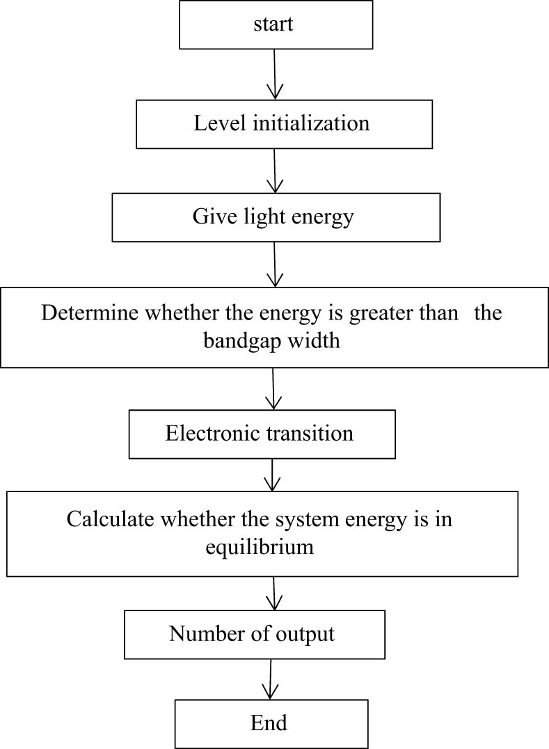
Flowchart of calculation program.
Figure 2 shows that when the light energy is small, there is a small difference in the number of carriers at different temperatures, but as the light energy increases, the higher the temperature, the lower the number of carriers. The more the number of carriers, the influence of temperature on the number of carriers increases. This may be due to the increase in light energy, the thermal movement of the particles in the system is intensified, the tendency of energy level interleaving increases, this promotes the narrowing of the bandgap of silicon semiconductors, therefore, it shows that under higher light energy, the influence of temperature on the number of carriers increases.
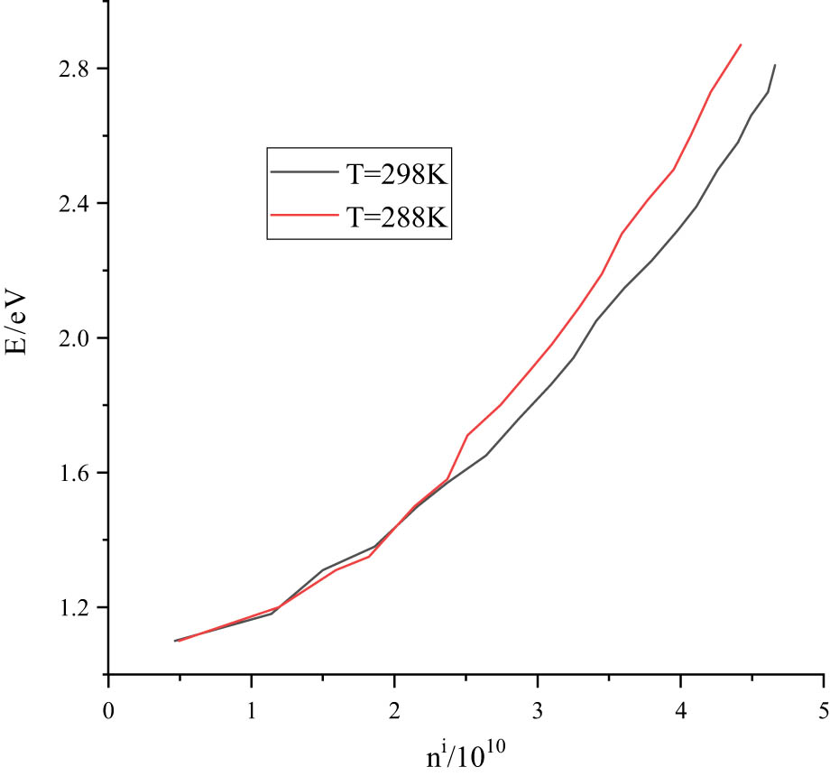
The influence of light energy E on the number of carriers
Figure 3 shows that the effect of temperature on the number of carriers is very obvious, in the temperature range studied (278–358 K); the changing trend is close to a straight line. This is consistent with the rapid increase of intrinsic carrier concentration with the increase of temperature in the actual semiconductor carrier distribution theory. This may be due to the approximate linear relationship between the forbidden bandwidth of most semiconductors and the temperature, and the significant increase of the thermodynamic entropy value of the system as the temperature increases.
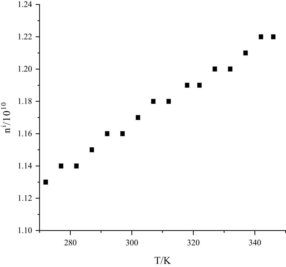
The influence of temperature T on the number of carriers n i .
For the main consideration of carrier drift in the active region, in terms of the single event effect of the diffusion and collection process, the calibrated structural parameters of the device are considered to reflect the radiation response of the device. For the total dose effect that mainly considers the charge trapping in the oxide layer, the inclination angle of the interface between the field oxide layer and the active region has a great influence on the sensitivity of the device’s total dose effect, but it hardly affects the normal characteristics of the device.
3 Discussion
The grand canonical ensemble is composed of a sample system that exchanges energy and quality independently with the outside world. According to the grand canonical distribution function, that is, the open system is in the process of time, the number of particles in the system is N, the probability of transition particles appearing at the energy level with energy E j (N) is as follows:
where
The basic thermodynamic function is as follows:
The grand canonical ensemble is a collection of N mutually independent specimen systems, the specimen systems are distinguishable, and the representative points that contain the system state in the same phase are not restricted [22]. If the specimen system contains only one particle, then this ensemble becomes a nearly independent particle system composed of N classical particles, and the system phase space becomes the particle phase space. At this time, E j (1) becomes the energy level of a particle and ε j , Ω j (1) becomes the degeneracy of the particle energy level ε j . From Eq. (16):
which is the probability of each particle of the system appearing at energy level
The amorphous silicon dioxide oxide layer is regarded as a wide bandgap semiconductor material under irradiation conditions. Gamma rays will induce a large number of non-equilibrium carriers inside the entire device. The unbalanced carriers generated in the silicon-doped region of the device will quickly recombine and annihilate the oxide layer, and the amorphous silicon dioxide–silicon interface contains a large amount of deep, shallow level defects and hydrogen impurities, complicated transport with the non-equilibrium carriers-reaction process. Therefore, the kinetic process of ionization damage mainly occurs in the oxide layer and interface area of the device [23].
The main dynamic mechanism of oxide ionization damage is summarized as follows:
Compton effect – gamma rays induce electron–hole pairs in the oxide layer area.
Dangling bond N it proton generation mechanism – electrons, holes, oxide layer defects, and hydrogen molecule (H2) undergo a series of complex reactions and the kinetic process of releasing protons.
N ot generation mechanism of oxide layer charged body defects – Deep-level defects in the oxide layer trap holes and formation of long-term stable charged body defects.
Depassivation effect – Protons are transported directionally to the S i O2–Si interface under the action of an electric field; it will act with the passivated Si–H bond. Revert to dangling bond (Si–), that is, the process of the N it defect of the charged interface, that is,
When we tested the electrical response of ionization damage, first the ionization damage model is simulated to obtain its specific physical parameters and then the obtained parameters are brought into the general semiconductor to simulate the electrical signal of the response; here, we briefly describe it. The numerical simulation of a general three-dimensional semiconductor device includes the Poisson equation describing the (2Si) electric field distribution in the silicon (Si) region:
where p is the hole concentration, N is the electron concentration,
The damage of ionization damage to the device is mainly divided into two categories: The first type is the trapped positive oxide charge
In view of the changes in surface carriers caused by ionization damage, it is necessary to add surface recombination caused by interface defect
where
Diffusion coefficient of movable particles in α-SiO2
| Particle type |
|
|
|
|
|---|---|---|---|---|
| Diffusion coefficient | 5 × 10⁻³ | 5 × 10⁻⁵ | 1 × 10⁻¹⁰ | 1 × 10⁻⁹ |
Numerical simulation of circuit-level radiation effects is an analytical method, refers to the form of describing the underlying devices (such as MOSFET and BJT) as compact models one by one, and determines the parameters in the model according to the specific process, by setting the external excitation of the device, the output current, and terminal voltage can be calculated analytically. This method has been widely used in the design process of the chip; it is usually used to verify the performance of the chip and as a basis for modifying the design [24]. The main idea of the radiation effect circuit simulation is to introduce the radiation effect into the transistor-level SPICE model. First, a single tube model is built that takes into account the radiation effect based on the radiation test data or device simulation data and then combined with commercial tools for circuit simulation. This is a practical technology that can combine basic research and industrialization [25,26]. In order to meet the requirements of electronic devices, circuit, and system radiation resistance hardening index requirements, the reinforcement performance should be accurately estimated at the beginning of the design. Circuit-level numerical simulation technology has played an important role in the prediction of radiation hardening ability, specifically, circuit-level total dose effect sensitivity simulation prediction and sensitive node identification, by constructing a SPICE model of the total dose effect of a single tube device in the complementary metal oxide semiconductor circuit of a 0.25 μm process, substituted into the internal circuit of 300,000 domestic static random-access memory (SRAM-type) field programmable gate arrays (FGPAs) to perform circuit simulation; finally, it is concluded that the most sensitive module of the FGPA is the power-on reset circuit, which was verified by the subsequent synchrotron radiation X microbeam experiment conducted at high energy. For single event effects, modified rise time is used and the fall time method is fitted to obtain the current pulse shape when the heavy-ion incident position deviates from the center of the collection junction of the drain region; the difference between the calculated single-event inversion cross section of the 65 nm SRAM device and the measured value is less than three times the measured value.
In terms of total dose effect circuit-level modeling and simulation, when building a single tube model, it usually corresponds to a single irradiation bias (the gate of the MOS tube is connected to the working voltage during the irradiation process), and in the following circuit simulation, all the transistors are set to uniformly add a single irradiation bias, and this is obviously not in line with the actual situation [27,28]. It is also impossible to use this method to investigate the response of the entire circuit to different irradiation biases. In response to this shortcoming, some organizations use manual screening methods to divide the transistors in some of the more important unit circuits, such as the single tube in the SRAM cell, according to the difference in irradiation bias, but this can only solve specific problems; it is required that the circuit bias state remains unchanged during the entire irradiation process, the circuit scale cannot be too large, and the single tubes in the circuit are in extreme states such as saturation or cut-off.
4 Conclusion
Using computer simulation methods, for the intrinsic silicon semiconductor in the grand canonical ensemble, through the study of the relationship between the light energy and the number of carriers, we get the following: at the same temperature, with the increase in light energy, the number of carriers gradually increases, but the magnitude of increase gradually decreases. When the light energy is small, there is a small difference in the number of carriers at different temperatures, but as the light energy increases, the higher the temperature, the more the number of carriers, the influence of temperature on the number of carriers increases. The study of the relationship between temperature and carrier number concluded that the temperature has a very obvious influence on the number of carriers, in the temperature range studied (278–358 K); the changing trend is close to a straight line. This result is basically consistent with the statistical distribution of semiconductor carriers; it can be seen that this method is suitable for the calculation of semiconductor carrier numbers, and it is an effective method for studying problems related to carrier distribution. On this basis, the author will continue to conduct further research on silicon semiconductors and other doped semiconductors. And through the drift diffusion-reaction model, the author describes the impact of trapped charges generated by ionization damage on semiconductor devices and gives the corresponding numerical method. The algorithm uses finite element discretization, implicit time method, and linearization method, to deal with the complex grid structure in the model and problems such as long-term evolution and strong nonlinearity. For different three-dimensional semiconductor devices, such as bipolar devices, the field-effect transistor carries out the corresponding simulation experiment of radiation damage, the numerical results that are consistent with the experimental results in the literature in terms of trend and magnitude are given; it reasonably reflects the impact of ionization damage on the electrical output characteristics of semiconductors. In addition, considering the application of radiation effect numerical simulation technology in complex electronic systems and engineering practices, it is also necessary to advance the numerical simulation of system-level radiation effects and discuss how to carry out performance evaluation for board-level systems and complex system-on-a-chip.
In view of the fruitful research results of the radiation effect research of semiconductor devices, combined with the semiconductor devices widely used in the industrial sector and technological field, this article briefly introduces the research trend of the radiation effect and points out the important research content involved in all aspects and the problems that need more in-depth research. The author is convinced that more intensive work on these trends will surely make more breakthroughs in the research field of the radiation effects of semiconductor devices.
-
Funding information: The authors state no funding involved.
-
Author contributions: All authors have accepted responsibility for the entire content of this manuscript and approved its submission.
-
Conflict of interest: The authors state no conflict of interest.
References
[1] Umegami H, Ishibashi H, Nanamori K, Hattori F, Yamamoto M. Basic analysis of false turn-on phenomenon of power semiconductor devices with parasitic inductances. Electron Lett. 2016;52(13):1158–60.10.1049/el.2016.1057Search in Google Scholar
[2] Islam A, Nakai T, Onodera H. Statistical analysis and modeling of random telegraph noise based on gate delay measurement. IEEE Trans Semicond Manuf. 2017;30(3):216–26.10.1109/TSM.2017.2715168Search in Google Scholar
[3] Schamel H, Eliasson B. On the correct implementation of fermi–dirac statistics and electron trapping in nonlinear electrostatic plane wave propagation in collisionless plasmas. Phys Plasmas. 2016;23(5):052114.10.1063/1.4949341Search in Google Scholar
[4] Rohde G, Stange A, Mueller A, Behrendt M, Oloff LP, Hanff K, et al. Decoding the ultrafast formation of a fermi–dirac distributed electron gas. Phys Rev Lett. 2018;121(25):256401.1–6.10.1103/PhysRevLett.121.256401Search in Google Scholar PubMed
[5] Yarmoghaddam E, Haratipour N, Koester SJ, Rakheja S. A physics-based compact model for ultrathin black phosphorus FETs--Part I: Effect of contacts, temperature, ambipolarity, and traps. IEEE Trans Electr Dev. 2019;67(8):389–96.10.1109/TED.2019.2951662Search in Google Scholar
[6] Shine G, Saraswat KC. Analysis of atomistic dopant variation and fermi level depinning in nanoscale contacts. IEEE Trans Electr Dev. 2017;64(9):3768–74.10.1109/TED.2017.2720183Search in Google Scholar
[7] Nagamura Y, Ide T, Arai M, Fukumoto S. Cnn-based layout segment classification for analysis of layout-induced failures. IEEE Trans Semicond Manuf. 2020;33(4):597–605.10.1109/TSM.2020.3029049Search in Google Scholar
[8] Kim HS, Kwon HJ, Lee SH, Dang JJ, Lee P, Yoon SP, et al. Upgrade plan of the komac proton linac for the atmospheric radiation test on semiconductor devices. J Korean Phys Soc. 2020;77(5):373–8.10.3938/jkps.77.373Search in Google Scholar
[9] Bai Y, Cai ZH, Wu YN, Chen S. Enhancing neutron radiation resistance of silicon-based semiconductor devices through isotope separation and enrichment. Radiat Eff Defects Solids. 2021;176(5–6):1–12.10.1080/10420150.2020.1855178Search in Google Scholar
[10] Bogatov NM, Grigorian LR, Kovalenko AI, Kovalenko MS, Lunin LS. Influence of radiation defects induced by low-energy protons at a temperature of 83 k on the characteristics of silicon photoelectric structures. Semiconductors. 2020;54(2):196–200.10.1134/S1063782620020062Search in Google Scholar
[11] Song Q, Chen H, Zhang M, Yin J, Yan P. Intensity-tunable terahertz radiation from tin selenide. J Lumin. 2021;235(2):118008.10.1016/j.jlumin.2021.118008Search in Google Scholar
[12] Sequeira MC, Mattei JG, Vazquez H, Djurabekova F, Lorenz K. Unravelling the secrets of the resistance of gan to strongly ionising radiation. Commun Phys. 2021;4(1):51.10.1038/s42005-021-00550-2Search in Google Scholar
[13] Garg N, Pratap Y, Gupta M, Kabra S. Reliability assessment of GaAs/Al2O3 junctionless finFET in the presence of interfacial layer defects and radiations. IEEE Trans Device Mater Reliab. 2020;20(2):452–8.10.1109/TDMR.2020.2991662Search in Google Scholar
[14] Shayesteh MR. Analysis of effect of singlet-triplet annihilation in a low-threshold optically pumped organic semiconductor laser. J Electron Mater. 2017;46(10):5664–9.10.1007/s11664-017-5624-4Search in Google Scholar
[15] Guo X, Zheng Q, Chi Z, Wang Z. Renormalization group analysis of ultracold fermi gases with two-body attractive interaction. Eur Phys J D. 2016;70(1):1–7.10.1140/epjd/e2015-60597-1Search in Google Scholar
[16] Usychenko VG, Sorokin LN, Usychenko AS. Penetration of electromagnetic radiation energy into a semiconductor element base of technical means without specialized receiving antennas. J Commun Technol Electron. 2020;65(12):1448–56.10.1134/S1064226920110170Search in Google Scholar
[17] Duinong M, Chee FP, Rasmidi R, Alias AB, Salleh S, Anuar K, et al. Gamma ray and neutron radiation effects on the electrical and structural properties of n-zno/p-cugao2 schottky diode. ECS J Solid State Sci Technol. 2020;9(4):045019.10.1149/2162-8777/ab8f19Search in Google Scholar
[18] Ismailov TA, Gadjiev HM, Ibragimova AM. Power-effective thermoelectric semiconductor heat rejection for computer processors. Her Dagestan State Tech Univ Tech Sci. 2020;47(3):8–15.10.21822/2073-6185-2020-47-3-8-15Search in Google Scholar
[19] Ruan DB, Liu PT, Gan KJ, Chiu YC, Sze SM. Role of tungsten dopants in indium oxide thin-film transistor on radiation hardness technology. Appl Phys Lett. 2020;116(18):182104.10.1063/1.5142557Search in Google Scholar
[20] Lee C, Cho G, Unruh T, Hur S, Kwon I. Integrated circuit design for radiation-hardened charge-sensitive amplifier survived up to 2 Mrad. Sensors. 2020;20(10):2765.10.3390/s20102765Search in Google Scholar PubMed PubMed Central
[21] Feng J, Li X, Hu J, Cai J. General vacuum electronics. J Electromagn Eng Sci. 2020;20(1):1–8.10.26866/jees.2020.20.1.1Search in Google Scholar
[22] Liu W, Li Z, Xing C, Wang R, Xu C. Thermal-assisted UV-photon irradiation to improve crystallization and luminescence efficiency of ZnO. IEEE Trans Electr Dev. 2021;68(7):3283–9.10.1109/TED.2021.3077207Search in Google Scholar
[23] Lee M, Cho S, Lee N, Kim J. Design for high reliability of CMOS IC with tolerance on total ionizing dose effect. IEEE Trans Dev Mater Reliab. 2020;20(2):459–67.10.1109/TDMR.2020.2994390Search in Google Scholar
[24] Xu X, Li L, Sharma A. Controlling messy errors in virtual reconstruction of random sports image capture points for complex systems. Int J Syst Assur Eng Manag. 2021;1.10.1007/s13198-021-01094-ySearch in Google Scholar
[25] Sharma A, Kumar R, Kaur P. Study of issues and challenges of different routing protocols in wireless sensor network. 2019 Fifth International Conference on Image Information Processing (ICIIP); 2019. Nov 15–17; Shimla, India. IEEE; 2020. p. 585–90.10.1109/ICIIP47207.2019.8985915Search in Google Scholar
[26] Liu Y, Sun Q, Sharma A, Sharma A, Dhiman G. Line monitoring and identification based on roadmap towards edge computing. Wirel Person Commun. 2021;4.10.1007/s11277-021-08272-ySearch in Google Scholar
[27] Yuvaraj N, Srihari K, Dhiman G, Somasundaram K, Masud M. Nature-inspired-based approach for automated cyberbullying classification on multimedia social networking. Math Probl Eng. 2021;2021:1–12.10.1155/2021/6644652Search in Google Scholar
[28] Kannan S, Dhiman G, Natarajan Y, Sharma A, Gheisari M. Ubiquitous vehicular ad-hoc network computing using deep neural network with iot-based bat agents for traffic management. Electronics. 2021;10(7):785.10.3390/electronics10070785Search in Google Scholar
© 2022 Zhanhan Hu et al., published by De Gruyter
This work is licensed under the Creative Commons Attribution 4.0 International License.
Articles in the same Issue
- Research Articles
- Fractal approach to the fluidity of a cement mortar
- Novel results on conformable Bessel functions
- The role of relaxation and retardation phenomenon of Oldroyd-B fluid flow through Stehfest’s and Tzou’s algorithms
- Damage identification of wind turbine blades based on dynamic characteristics
- Improving nonlinear behavior and tensile and compressive strengths of sustainable lightweight concrete using waste glass powder, nanosilica, and recycled polypropylene fiber
- Two-point nonlocal nonlinear fractional boundary value problem with Caputo derivative: Analysis and numerical solution
- Construction of optical solitons of Radhakrishnan–Kundu–Lakshmanan equation in birefringent fibers
- Dynamics and simulations of discretized Caputo-conformable fractional-order Lotka–Volterra models
- Research on facial expression recognition based on an improved fusion algorithm
- N-dimensional quintic B-spline functions for solving n-dimensional partial differential equations
- Solution of two-dimensional fractional diffusion equation by a novel hybrid D(TQ) method
- Investigation of three-dimensional hybrid nanofluid flow affected by nonuniform MHD over exponential stretching/shrinking plate
- Solution for a rotational pendulum system by the Rach–Adomian–Meyers decomposition method
- Study on the technical parameters model of the functional components of cone crushers
- Using Krasnoselskii's theorem to investigate the Cauchy and neutral fractional q-integro-differential equation via numerical technique
- Smear character recognition method of side-end power meter based on PCA image enhancement
- Significance of adding titanium dioxide nanoparticles to an existing distilled water conveying aluminum oxide and zinc oxide nanoparticles: Scrutinization of chemical reactive ternary-hybrid nanofluid due to bioconvection on a convectively heated surface
- An analytical approach for Shehu transform on fractional coupled 1D, 2D and 3D Burgers’ equations
- Exploration of the dynamics of hyperbolic tangent fluid through a tapered asymmetric porous channel
- Bond behavior of recycled coarse aggregate concrete with rebar after freeze–thaw cycles: Finite element nonlinear analysis
- Edge detection using nonlinear structure tensor
- Synchronizing a synchronverter to an unbalanced power grid using sequence component decomposition
- Distinguishability criteria of conformable hybrid linear systems
- A new computational investigation to the new exact solutions of (3 + 1)-dimensional WKdV equations via two novel procedures arising in shallow water magnetohydrodynamics
- A passive verses active exposure of mathematical smoking model: A role for optimal and dynamical control
- A new analytical method to simulate the mutual impact of space-time memory indices embedded in (1 + 2)-physical models
- Exploration of peristaltic pumping of Casson fluid flow through a porous peripheral layer in a channel
- Investigation of optimized ELM using Invasive Weed-optimization and Cuckoo-Search optimization
- Analytical analysis for non-homogeneous two-layer functionally graded material
- Investigation of critical load of structures using modified energy method in nonlinear-geometry solid mechanics problems
- Thermal and multi-boiling analysis of a rectangular porous fin: A spectral approach
- The path planning of collision avoidance for an unmanned ship navigating in waterways based on an artificial neural network
- Shear bond and compressive strength of clay stabilised with lime/cement jet grouting and deep mixing: A case of Norvik, Nynäshamn
- Communication
- Results for the heat transfer of a fin with exponential-law temperature-dependent thermal conductivity and power-law temperature-dependent heat transfer coefficients
- Special Issue: Recent trends and emergence of technology in nonlinear engineering and its applications - Part I
- Research on fault detection and identification methods of nonlinear dynamic process based on ICA
- Multi-objective optimization design of steel structure building energy consumption simulation based on genetic algorithm
- Study on modal parameter identification of engineering structures based on nonlinear characteristics
- On-line monitoring of steel ball stamping by mechatronics cold heading equipment based on PVDF polymer sensing material
- Vibration signal acquisition and computer simulation detection of mechanical equipment failure
- Development of a CPU-GPU heterogeneous platform based on a nonlinear parallel algorithm
- A GA-BP neural network for nonlinear time-series forecasting and its application in cigarette sales forecast
- Analysis of radiation effects of semiconductor devices based on numerical simulation Fermi–Dirac
- Design of motion-assisted training control system based on nonlinear mechanics
- Nonlinear discrete system model of tobacco supply chain information
- Performance degradation detection method of aeroengine fuel metering device
- Research on contour feature extraction method of multiple sports images based on nonlinear mechanics
- Design and implementation of Internet-of-Things software monitoring and early warning system based on nonlinear technology
- Application of nonlinear adaptive technology in GPS positioning trajectory of ship navigation
- Real-time control of laboratory information system based on nonlinear programming
- Software engineering defect detection and classification system based on artificial intelligence
- Vibration signal collection and analysis of mechanical equipment failure based on computer simulation detection
- Fractal analysis of retinal vasculature in relation with retinal diseases – an machine learning approach
- Application of programmable logic control in the nonlinear machine automation control using numerical control technology
- Application of nonlinear recursion equation in network security risk detection
- Study on mechanical maintenance method of ballasted track of high-speed railway based on nonlinear discrete element theory
- Optimal control and nonlinear numerical simulation analysis of tunnel rock deformation parameters
- Nonlinear reliability of urban rail transit network connectivity based on computer aided design and topology
- Optimization of target acquisition and sorting for object-finding multi-manipulator based on open MV vision
- Nonlinear numerical simulation of dynamic response of pile site and pile foundation under earthquake
- Research on stability of hydraulic system based on nonlinear PID control
- Design and simulation of vehicle vibration test based on virtual reality technology
- Nonlinear parameter optimization method for high-resolution monitoring of marine environment
- Mobile app for COVID-19 patient education – Development process using the analysis, design, development, implementation, and evaluation models
- Internet of Things-based smart vehicles design of bio-inspired algorithms using artificial intelligence charging system
- Construction vibration risk assessment of engineering projects based on nonlinear feature algorithm
- Application of third-order nonlinear optical materials in complex crystalline chemical reactions of borates
- Evaluation of LoRa nodes for long-range communication
- Secret information security system in computer network based on Bayesian classification and nonlinear algorithm
- Experimental and simulation research on the difference in motion technology levels based on nonlinear characteristics
- Research on computer 3D image encryption processing based on the nonlinear algorithm
- Outage probability for a multiuser NOMA-based network using energy harvesting relays