Strip waveguides in Yb3+-doped silicate glass formed by combination of He+ ion implantation and precise ultrashort pulse laser ablation
-
 ,
,

Abstract
Strip optical waveguides were realized in Yb3+-doped silicate glass with ultrashort pulse laser ablation assisted He+ ion implantation. Planar waveguides were first prepared near the glass surface by He+ ion implantation (450 keV + 500 keV + 550 keV), followed by annealing at 260℃. After that, under the processing parameters of 3 μJ energy and 50 μm/s ablation velocity, two parallel tracks with separation of 15, 20, and 25 μm were, respectively, inscribed on the sample, which confine the light in lateral direction to form a strip waveguide. The near-field intensity measurement indicates that the strip waveguides maintain the single-mode propagation characteristics with 976 nm laser injection, and present the multi-mode characteristics with 632.8 nm laser injection, showing that the guided modes are well supported in the strip waveguides. The minimum propagation loss of strip waveguide is 1.35 dB/cm. Fluorescence emission spectra indicate that the gain properties of waveguide core were maintained well after waveguide preparation, revealing that the strip waveguide device in Yb3+-doped silicate glass has the potential to become an active device as waveguide laser or waveguide amplifier.
1 Introduction
Integrated photonic devices [1,2,3,4,5,6], due to their compact size, low insertion loss, various functions ,and low power consumption, have attracted much attention in recent years. As the most basic integrated photonic component, optical waveguides can not only connect various photonic devices in series and provide basic functions such as coupling, routing, and polarization [7,8,9,10], but also present enhanced optical properties (optical amplification, lasing, nonlinearity, etc.) [11,12,13,14], which is due to the fact that optical waveguides confine light propagation in a small volume compared with light beam propagation in bulk media. Among these optical waveguide devices, active gain waveguides (waveguide lasers and waveguide amplifiers), which provide the light source of the whole integrated optical circuit, is responsible for promoting the integration of photonic chips [15,16]. Compared with the traditional solid-state lasers with bulk gain media, the active gain waveguides have higher pump laser power density and higher degree of overlap between pump beam and signal beam due to the confinement of their waveguide structures. In addition, with appropriate parameters of laser cavity mirrors, the pump threshold will be greatly reduced. Consequently, the key to realize waveguide laser or waveguide amplifier in gain media is to prepare high-quality waveguide and maintain the active gain characteristics of waveguide region.
Rare earth ions, as important doped ions, play a role in providing laser emission in solid-state laser materials. Yb3+ ions have attracted extensive attention due to the fact that the emission spectrum ranges from 0.9 to 1.1 μm in the near-infrared band. Recently, the rapid improvement in ion doping technology in different optical media has promoted the emergence of many excellent laser dielectric materials. Among them, Yb3+-doped silicate glass is a representative laser material with high thermal stability and high laser damage threshold [17]. In addition, combined with the lattice structure properties of silicate glass substrate materials, Yb3+ ions in silicate glass show the characteristics of narrow-band absorption spectrum and wide-band emission spectrum. The low energy state 2F7/2 and high energy state 2F5/2 constitute the simple electronic energy level scheme of Yb ions, which allows Yb3+ ions to be highly doped in silicate glass without concentration quenching. Furthermore, the millisecond fluorescence lifetime of Yb3+ ions in silicate glass is favorable to obtain higher pulse energy in Q-switched pulse lasers and Q-switched pulse amplifiers. Therefore, Yb3+-doped silicate glass is an ideal substrate material for the preparation of active photonic devices.
Recently, various preparation techniques have been adopted to obtain high-quality optical waveguides in different material substrates, such as ion exchange [18,19], ion implantation [20,21,22,23], laser direct writing [24,25,26], and so on. Ion implantation, which can introduce charged ions with energy of hundreds of keV to several MeV into the near surface region of the substrate material and cause the modulation of refractive index to form a waveguide structure, is a widely used waveguide fabrication method. Moreover, during the implantation process, the energy and dose of ions can be accurately controlled [27], which allows the refractive index to be regulated. In addition, in general, the performance of the materials were well maintained in the region of ion implantation [28]. However, the waveguide prepared by ion implantation without any auxiliary means is only one-dimensional planar waveguide structure. This one-dimensional waveguide structure confines light only in the vertical direction, which will lead to lower light intensity and low coupling efficiency in the cascade with photonic devices such as optical fibers. Therefore, the two-dimensional (2D) structure waveguide, which can improve the interconnection efficiency of various devices, shows great advantages in the integrated optical circuit. Ultrashort pulse laser ablation assisted ion implantation is a powerful method to fabricate strip waveguides [29,30,31]. Following the step of forming a planar waveguide by ion implantation, the laser beam with high peak power is concentrated into a tiny volume in the waveguide region, and then the local material will be removed due to the strong interaction between the laser and the material induced by nonlinear absorption. In the whole process, due to the localization of nonlinear absorption and ultrashort interaction time, the materials outside the focus area will not be affected. In addition, different from the traditional mask-assisted ion implantation process, which needs to replace the masks with different structures to meet the preparation requirements of waveguides with different sizes, femtosecond laser ablation assisted ion implantation can easily realize strip waveguides of different sizes only by the relative movement between the laser focus and the sample. Moreover, the strip waveguide with complex 2D structure, such as curved 2D waveguide, waveguide couplers, waveguide beam splitters, etc., can be easily realized by femtosecond laser ablation, which allows it to become a powerful means of 2D waveguide preparation. Therefore, ultrashort pulse laser ablation assisted ion implantation technology effectively integrates the advantages of the two preparation technologies, and provides an economic, convenient, and efficient solution for 2D waveguide preparation.
In integrated optics, low insertion loss cascading with small-scale photonic devices requires a planar waveguide structure with a thinner core layer. He+ ion implantation and H+ ion implantation, both of which are typical light ion implantation, are commonly used to form planar waveguides in different optical materials due to their relatively negligible perturbation to the lattice structure of the substrate. In general, under the same irradiation energy, the penetration depth of He+ ions is less than that of H+ ions, and the depth of the optical barrier formed by He+ ions is also less than that of the optical barrier formed by H+ ions. Therefore, it is easy for He+ ion implantation to form planar waveguides with small core layers. In this work, the strip waveguides have been successfully prepared in Yb3+-doped silicate glass by He+ ion implantation combined with ultrashort pulse laser ablation technology for the first time, to our knowledge. The vacancy distribution in the planar waveguide implanted with He+ ions was numerically analyzed. The end face morphologies and guided mode characteristics of waveguides with different laser ablation parameters were systematically investigated. The results indicate that the waveguides support single-mode propagation with 976 nm laser injection and the multi-mode propagation with 632.8 nm laser injection. The propagation loss of the strip waveguide can reach the lowest value of 1.35 dB/cm. The micro-fluorescence measurement shows that the laser properties of the material were well preserved after the waveguide preparation process. These properties provide the potential to fabricate active photonic devices in the future.
2 Experimental setup
The Yb3+-doped silicate glass sample (2 mol% Yb2O3) was obtained from Xi′an Institute of Optics and Precision Mechanics of Chinese Academy of Sciences. In order to facilitate waveguide processing (ion implantation and laser ablation), the sample was cut into a size of 10 mm × 6 mm × 2 mm and optically polished. The first step in the preparation of 2D waveguide is to construct a planar optical waveguide by triple energy (450 keV + 500 keV + 550 keV) He+ ion implantation in the region below the sample surface. Figure 1(a) shows a schematic diagram of He+ ions implantation to form a planar optical waveguide, in which 450 keV He+ ions (2 × 10¹⁶ ions/cm2) were first implanted into the top surface of the sample, and then 500 and 550 keV He+ ions with the same dose (2 × 10¹⁶ ions/cm2) were sequentially implanted into the surface of the sample to obtain a broadband barrier and optimize the tunnel loss. It should be pointed out here that in the process of triple ion implantation, the ion beam current densities have been strictly controlled at a low level to avoid the impact of thermal effect. Then, after the ion implantation process, the planar waveguide samples were annealed for 60 min in an air environment at 260℃ for elimination of internal damage of materials release and low waveguide propagation loss.

(a) Optical waveguide preparation by triple energy He+ ion implantation; (b) strip waveguide preparation with ultrashort pulse laser ablation technology.
The second processing step is to ablate with ultrafast laser to form strip waveguide, as depicted in Figure 1(b). The Ti3+:sapphire CPA amplification system (Spitfire, SP) delivers laser pulses (808 nm, 1 kHz) to the sample surface by an objective lens, and the pulse width was measured to be 150 fs behind the objective lens. A 1/2λ plate followed by a polarizer were placed in front of the focusing microscope objective to adjust the laser energy delivered onto the planar waveguide. It is worth mentioning that the laser energy irradiated on the sample is measured after the microscope objective. In our experiment, the pulse energy was set to a moderate value of 3 μJ, and the scan speed was 50 μm/s, which means that 20 pulses are deposited in the range of 1 μm.
With such processing parameters, the size of the ablation groove at the track of the laser focus presents a moderate morphology, which can meet the requirements of cutting through the planar waveguide without causing wider damage. In order to confine the light on both sides of the horizontal direction of the planar waveguide, two parallel ablation grooves were constructed to realize the strip waveguide structure. Parallel ablation grooves with double line spacing of 15, 20, and 25 μm were inscribed on the sample surface, respectively.
A charge coupled device (CCD) camera on an optical transmission microscope was employed to record the morphology image of the prepared planar waveguide. An end coupling measurement system, as depicted in Figure 2, was employed to investigate the guided mode characteristics of planar waveguides. The 976 nm laser is injected into the waveguide input with a 20× objective. At the other end of the waveguide, the light intensity at the output end of the waveguide is collected using a microscope objective with the same focal length (f = 10 mm) and imaged onto the CCD camera. All lenses and sample mentioned above were mounted on the 6D optical precision stage for easy adjustment.
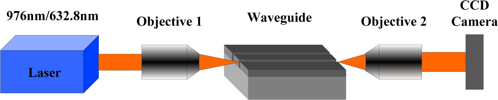
The schematic of the experimental setup for near-field intensity measurement. The coupling laser sources are 976 nm LD laser and 632.8 nm He–Ne laser.
3 Results and discussion
3.1 The vacancy distribution
The vacancy distribution of planar optical waveguides formed by (450 keV + 500 keV + 550 keV) He+ ion implantation is numerically simulated by SRIM 2013 [32]. The vacancy distributions corresponding to ion implantation conditions with He+ ion energy of 450, 500, and 550 keV and the total vacancy distribution are, respectively, illustrated in Figure 3. The vacancy distribution is a function of depth from the surface, and the corresponding vacancy distribution depth increases with the increase in the energy of implanted ions. The corresponding depth of 550 keV ion implantation exceeds 2 μm, which indicates that the triple energy ion implantation can effectively increase the coverage depth of vacancy distribution. As can be seen in Figure 3, the total vacancy distribution reaches a maximum value of 0.0015 at a depth of 1.86 μm.
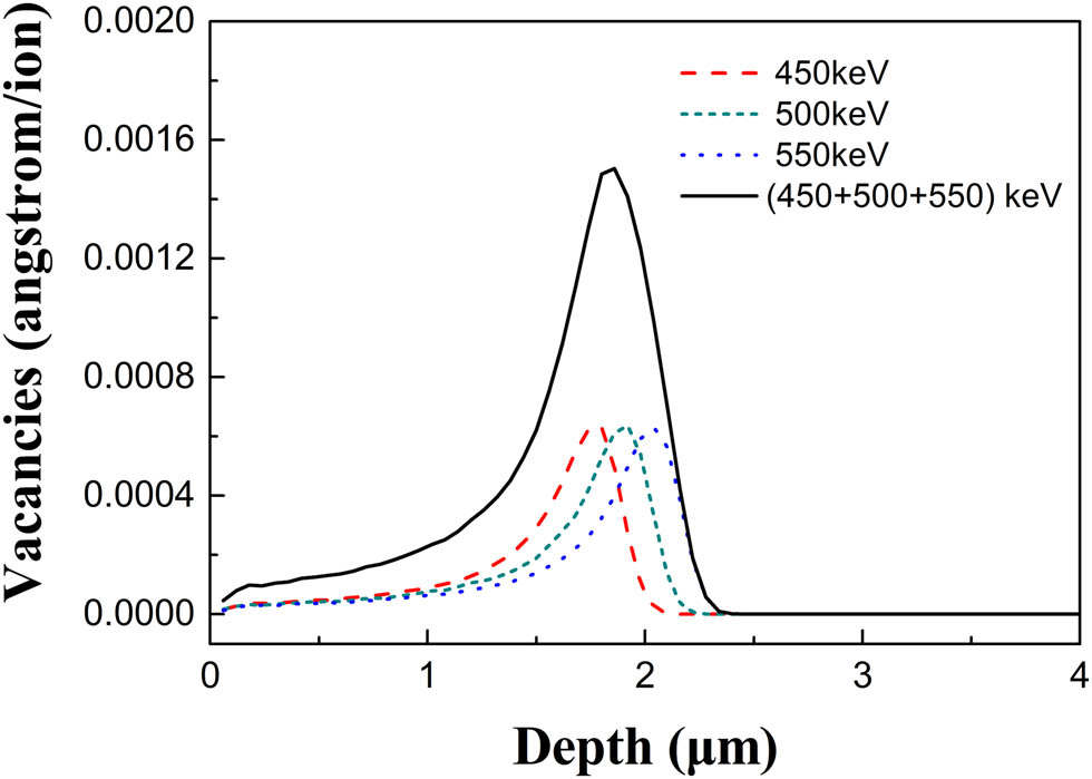
Vacancy distributions of waveguides fabricated under different ion implantation conditions.
The mechanism of refractive index modification can be explained by the interaction between He+ ions and substrate during ion implantation [33,34,35,36]. According to the movement process of He+ ions, the region near the sample surface can be divided into two regions, one is the region swept by the movement track of He+ ions, and the other is the region where the end of the movement track of He+ ions is located, that is, the deposition region of He+ ions.
In the first region, high-speed implanted ions often transfer energy to the matrix material through inelastic collision and ionization, resulting in local refractive index modification. In view of the light mass of He+ ions, the energy transfer of collision can be ignored and only the effect of ionization (e.g., Si–O bond breaking) on the refractive index can be considered [34]. In the ionization process, the breaking of the bond of the host material will lead to volume compression and densification, resulting in the refractive index in the He+ ion movement trace being higher than that in the surrounding area. In addition, as mentioned in ref. [35], the volume compression caused by ionization will be easily saturated at a low value. Eventually, there will be a slight increase in the refractive index in this region, thus forming a “well” for the beam.
Almost at the same time, the implanted light He+ ions are distributed at the end of the trace, replacing the original ions in the base material, such as Na+ ions, which will form relative vacancies and reduce the local density. Finally, this will form a low refractive index cladding as a “barrier” for the guided mode. Combined with the air cladding on the sample surface and the above two refractive index modification mechanisms, the refractive index distribution forms a typical “well + barrier” region. In this way, a planar optical waveguide is realized, which confines the light in the region below the surface.
3.2 Waveguide morphology and guided-mode properties
In order to form a strip waveguide with sufficient ablation depth without causing extensive damage, the pulse energy is strictly controlled at 3 μJ during the whole laser processing process, as mentioned in Section 2. At the same time, the scan speed of the pulsed beam is fixed at 50 μm/s, which means that about 20 pulses are deposited in the range of 1 μm, averagely. Finally, two parallel air grooves form the waveguide cladding in the horizontal direction, and then the strip waveguide is constructed. In the experiment, the double line spacing of 15, 20, and 25 μm were investigated, respectively. Figure 4 shows the top view and end view optical micrograph of the morphologies of the strip waveguides with different double line spacings. The shapes of the double grooves are uniform and parallel, as depicted in Figure 4(a–c). Figure 4(d–f) shows that the depth of the air groove is 3.5 μm, which is enough to confine the guided mode in the horizontal direction. Combined with the optical confinement in the vertical direction, a strip waveguide can be formed. It is worth mentioning here that the stress distribution will appear near the air groove ablated by laser, which will compress the volume of the medium around the groove and improve the local density, and finally increase the refractive index slightly.
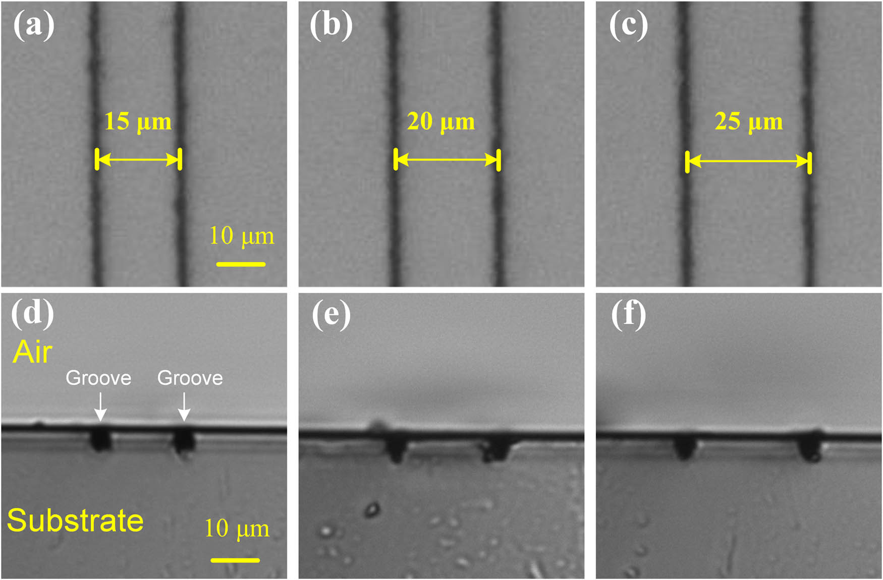
The top view (a–c) and end view (d–f) microphotographs of the morphologies of the strip optical waveguides with different double line spacings.
In the end coupling measurement system, a 976 nm laser and a 632.8 nm laser are used as coupling light sources, respectively. A 20× objective lens (coated with antireflective film in the band of 600–1,100 nm) delivers the laser to the waveguide. At the other end of the waveguide, the output laser will be collected and imaged on the CCD camera by an objective lens with the same focal length (f = 10 mm). Figure 5(a–c) shows the near-field mode intensity images of planar waveguides with transverse widths of 15, 20, and 25 μm at 976 nm laser injection. It represents that the transverse dimension of the guided mode increases with the double line spacing, but still maintains the single-mode propagation characteristics.

The near-field intensity distributions of the guided (a–c) 976 nm laser and (d–f) 632.8 nm laser of the strip waveguide with different waveguide widths ranging from 15 to 25 μm.
While maintaining other experimental measurement conditions, only the injected laser was replaced with the 632.8 nm He–Ne laser for the measurement of near-field mode. Figure 5(d–f) depicts the guided-mode images of strip waveguides with double line spacing of 15, 20, and 25 μm under this 632.8 nm injection condition, respectively. Figure 5(d) shows that few mode propagations in the horizontal direction have been supported in a waveguide with a transverse width of 15 μm. Figure 5(e) and (f) shows that as the waveguide width increases, higher-order modes emerge in the horizontal direction. The results show that under the condition of 632.8 nm injection, the beam is still well confined in the waveguide region. More importantly, the emergence of higher-order modes under short wavelength injection conditions also provides a means of waveguide mode conversion, such as waveguide mode converter. The abovementioned single-mode and multi-mode near-field intensity distributions are also consistent with the structural characteristics of planar waveguides.
The refractive index modification of planar waveguide core caused by He+ ion implantation can be roughly estimated by the measurement of the waveguide numerical aperture. Based on the end coupling measurement system, an iris with adjustable aperture is placed in front of the input coupling lens. By carefully adjusting the diameter of the iris, the maximum incident angle of the waveguide can be obtained. The refractive index modification (
where
With the same end coupling system, the propagation loss of the strip waveguides can also be estimated by the insertion loss of the waveguide. In order to eliminate the influence of Yb3+ ions absorption on the insertion loss measurement, here we choose 1,053 nm fiber laser as the injection light source (outside the absorption band of the Yb3+ ions). Considering the transmittance of the objective lens used in the experiment (>90% at 1,053 nm), the total insertion losses of the guided modes of the three strip waveguides with widths of 15, 20, and 25 μm are 1.51, 1.4, and 1.35 dB, respectively. In view of the inevitable coupling loss, the propagation loss of three waveguides with different widths must be less than 1.51, 1.4, and 1.35 dB/cm. The propagation loss originates from the scattering caused by the inconsistency of the waveguide region, in which the non-uniformity of air grooves ablated by the ultrashort pulse laser plays a more important role compared with the He+ ions interaction region.
3.3 Micro-fluorescence properties
To find out whether the strip waveguide preparation process affects the active gain properties of waveguide core, the micro-fluorescence measurement system is arranged to obtain the fluorescence spectrum in the waveguide core and the substrate. The 976 nm fiber pigtailed laser diode as a near-field mode measurement light source is used here as an excitation light source. Based on the end coupling system in near-field mode measurement, the coupling objective was replaced by 40× micro-objective lens in order to reduce the focus size of pump laser, which can avoid the excitation of the region outside the waveguide core. A single-mode fiber was placed on the upper side of the planar waveguide to collect the fluorescence spectrum in the optical spectrum analyzer.
As shown in Figure 6, the red solid line and the black solid line represent the fluorescence spectra of the waveguide core layer and the substrate, respectively. It can be seen that the emission spectra of the two regions are basically the same in shape, including the similar spectral range from 930 to 1,120 nm and the peak located at 1,016 nm. The results indicate that the emission spectrum of Yb3+-doped silicate glass is basically not affected by the fabrication process. This advantage can be attributed to two reasons. One is that the dose of He+ ions in the waveguide region is very low without causing major structural modifications. The other is that the closed electron shell of Yb3+ ions can shield the inner electron energy level responsible for the transition and emitting photons from the external energy (energy deposition of ion implantation and laser ablation induced stress). In Figure 6, it can be seen that some slight differences exist between the two curves, which is due to the ionization of implanted ions on the glass substrate material (the breaking of Si–O bond) and the stress induced by laser ablation. Both of these two effects will produce volume compression and small modification of the glass network, which will affect some details of the fluorescence emission spectrum. In general, the maintenance of this fluorescence characteristic after the waveguide preparation process provides the possibility of preparing active photonic devices in the future.
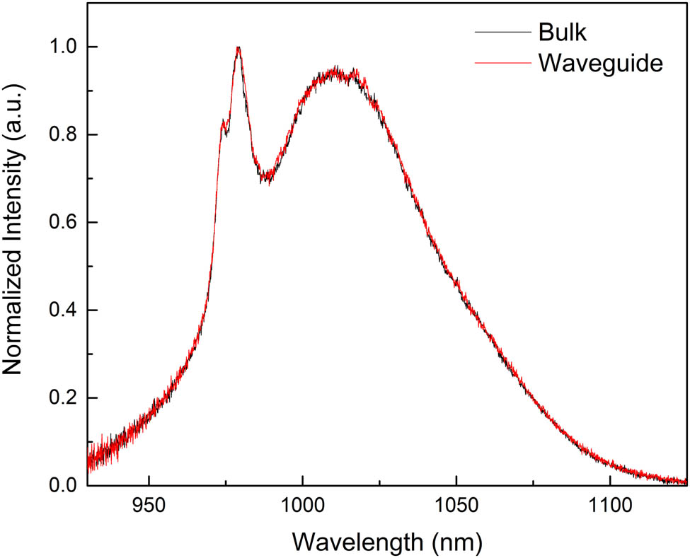
Comparison of fluorescence spectra between strip waveguide core layer and substrate excited by 976 nm laser diode.
4 Conclusion
In conclusion, to our knowledge, for the first time, we have demonstrated the preparation of strip waveguides in Yb3+-doped silicate glass by triple energy He+ ion implantation combined with laser ablation. With the formation of vacancies induced by He+ ion deposition and the energy deposition in the ion implantation trace, a typical potential “well + barrier” is formed. The simulation results show that the vacancy layer appears at a depth of 2 μm below the glass surface, which is approximately the thickness of the planar waveguide. Three strip waveguides with different widths were investigated in detail in terms of morphology and near-field mode. The results show that under 976 nm injection condition, the waveguides of three widths only support the single-mode propagation, but under 632.8 nm injection condition, few modes can be propagated in the strip waveguides. The minimum propagation loss of strip waveguide is 1.35 dB/cm. The results of micro-fluorescence spectra confirms that the waveguide preparation has no effect on the fluorescence emission characteristics of the substrate material, and the active gain characteristics are well maintained. This work points out that the preparation of waveguides by ion implantation combined with laser ablation is a practical method for the preparation of active gain photonic devices.
-
Funding information: The work is supported by the Scientific and Technological Innovation Programs of Higher Education Institutions in Shanxi (No. 2021L421), the National Natural Science Foundation of China (62075238), and the Doctoral Scientific Research Foundation of Hunan University of Medicine in China (No. 2020122002).
-
Author contributions: All authors have accepted responsibility for the entire content of this manuscript and approved its submission.
-
Conflict of interest: The authors state no conflict of interest.
References
[1] Murphy EJ. Integrated optical circuits and components: Design and applications. New York: Marcel Dekker; 1999.Search in Google Scholar
[2] Jean P, Douaud A, LaRochelle S, Messaddeq Y, Shi W. Templated dewetting for self-assembled ultra-low-loss chalcogenide integrated photonics. Opt Mater Exp. 2021;11(11):3717–35.10.1364/OME.443648Search in Google Scholar
[3] Urbonas D, Mahrt RF, Stöferle T. Low-loss optical waveguides made with a high-loss material. Light Sci Appl. 2021;10(1):1–7.10.1038/s41377-020-00454-wSearch in Google Scholar PubMed PubMed Central
[4] Li LQ, Nie WJ, Li ZQ, Romero C, Rodriguez-Beltrán RI, Vázquez de Aldana JR, et al. Laser-writing of ring-shaped waveguides in BGO crystal for telecommunication band. Opt Exp. 2017;25(20):24236–41.10.1364/OE.25.024236Search in Google Scholar PubMed
[5] Hendriks WAPM, Chang LT, van Emmerik CI, Mu JF, de Goede M, Dijkstra M, et al. Rare-earth ion doped Al2O3 for active integrated photonics. Adv Phys X. 2021;6(1):1833753.10.1080/23746149.2020.1833753Search in Google Scholar
[6] Wang XB, Zhang ML, Jiang MH, Lian TH, Wang F, Zhang DM. Monolithic integrated waveguide device with dual functions of electro-optic modulation and optical amplification. Opt Lett. 2021;46(15):3536–9.10.1364/OL.433818Search in Google Scholar PubMed
[7] Hu CR, Pan A, Li TA, Wang XH, Liu YH, Tao SQ, et al. High-efficient coupler for thin-film lithium niobate waveguide devices. Opt Exp. 2021;29(4):5397–406.10.1364/OE.416492Search in Google Scholar PubMed
[8] Yang XG, Wen L, Yan JH, Bao YJ, Chen Q, Camposeo A, et al. Energy dissipation and asymmetric excitation in hybrid waveguides for routing and coloring. J Phys Chem Lett. 2021;12(29):7034–40.10.1021/acs.jpclett.1c01690Search in Google Scholar PubMed
[9] Morichetti F, Milanizadeh M, Petrini M, Zanetto F, Ferrari G, de Aguiar DO, et al. Polarization-transparent silicon photonic add-drop multiplexer with wideband hitless tuneability. Nat Commun. 2021;12(1):1–7.10.1038/s41467-021-24640-5Search in Google Scholar PubMed PubMed Central
[10] Bai J, Cheng GH, Long XW, Wang YS, Zhao W, Chen GF, et al. Polarization behavior of femtosecond laser written optical waveguides in Ti:sapphire. Opt Exp. 2012;20(14):15035–44.10.1364/OE.20.015035Search in Google Scholar PubMed
[11] Li LQ, Li ZQ, Nie WJ, Romero C, Vázquez de Aldana JR, Chen F. Femtosecond-laser-written s-curved waveguide in Nd:YAP crystal: Fabrication and multi-gigahertz lasing. J Lightwave Technol. 2020;38(24):6845–52.10.1109/JLT.2020.3015690Search in Google Scholar
[12] Qu B, Wang SB, Zhu ZD, Hui YL, Lei H, Li Q. Symmetrical corner-pumped planar waveguide laser amplifier. IEEE J Quantum Electron. 2021;57(5):1–8.10.1109/JQE.2021.3102823Search in Google Scholar
[13] Chen ZX, Xu Q, Zhang K, Wong WH, Zhang DL, Pun EYB, et al. Efficient erbium-doped thin-film lithium niobate waveguide amplifiers. Opt Lett. 2021;46(5):1161–4.10.1364/OL.420250Search in Google Scholar PubMed
[14] Carvalho DO, Kassab LRP, Del Cacho VD, da Silva DM, Alayo MI. A review on pedestal waveguides for low loss optical guiding, optical amplifiers and nonlinear optics applications. J Lumin. 2018;203:135–44.10.1016/j.jlumin.2018.06.037Search in Google Scholar
[15] Grivas C. Optically pumped planar waveguide lasers, part I: Fundamentals and fabrication techniques. Prog Quantum Electron. 2011;35(6):159–239.10.1016/j.pquantelec.2011.05.002Search in Google Scholar
[16] Bradley JDB, Pollnau M. Erbium‐doped integrated waveguide amplifiers and lasers. Laser Photonics Rev. 2011;5(3):368–403.10.1002/lpor.201000015Search in Google Scholar
[17] Boulon G. Why so deep research on Yb3+-doped optical inorganic materials? J Alloy Compd. 2008;451(1–2):1–11.10.1016/j.jallcom.2007.04.148Search in Google Scholar
[18] Tervonen A, Honkanen SK, West BR. Ion-exchanged glass waveguide technology: A review. Opt Eng. 2011;50(7):071107.10.1117/1.3559213Search in Google Scholar
[19] Broquin JE, Honkanen S. Integrated photonics on glass: A review of the ion-exchange technology achievements. Appl Sci. 2021;11(10):4472.10.3390/app11104472Search in Google Scholar
[20] Wang YS, Chen BK, Huang X, Ding WJ, Yue QY, Liu CX. Optical properties and thermal stability of the H+-implanted Dy3+/Tm3+-codoped GeS2–Ga2S3–PbI2 chalcohalide glass waveguide. Open Phys. 2022;20(1):458–63.10.1515/phys-2022-0045Search in Google Scholar
[21] Chen F. Micro-and submicrometric waveguiding structures in optical crystals produced by ion beams for photonic applications. Laser Photonics Rev. 2012;6(5):622–40.10.1002/lpor.201100037Search in Google Scholar
[22] Shen JP, Lv JY, Chen JY, Xu J, Liu CX. Proton-implanted waveguides in neodymium-doped calcium lithium niobium gallium garnet crystals. Results Phys. 2019;15:102794.10.1016/j.rinp.2019.102794Search in Google Scholar
[23] Chen JY, Xie ZH, Li WN, Lin SB, Zhang LL, Liu CX. Construction and investigation of a planar waveguide in photo-thermal-refractive glass by proton implantation. Optik. 2020;207:164461.10.1016/j.ijleo.2020.164461Search in Google Scholar
[24] Bai J, Long XW, Liu X, Huo GW, Zhao W, Stoian R, et al. Embedded optical waveguides fabricated in SF10 glass by low-repetition-rate ultrafast laser. Appl Opt. 2013;52(30):7288–94.10.1364/AO.52.007288Search in Google Scholar PubMed
[25] Long XW, Bai J, Zhao W, Stoian R, Hui RQ, Cheng GH. Stressed waveguides with tubular depressed-cladding inscribed in phosphate glasses by femtosecond hollow laser beams. Opt Lett. 2012;37(15):3138–40.10.1364/OL.37.003138Search in Google Scholar PubMed
[26] Heilmann R, Greganti C, Gräfe M, Nolte S, Walther P, Szameit A. Tapering of femtosecond laser-written waveguides. Appl Opt. 2018;57(3):377–81.10.1364/AO.57.000377Search in Google Scholar PubMed
[27] Tan Y, Chen F, Stepić M, Shandarov V, Kip D. Reconfigurable optical channel waveguides in lithium niobate crystals produced by combination of low-dose O3+ ion implantation and selective white light illumination. Opt Exp. 2008;16(14):10465–70.10.1364/OE.16.010465Search in Google Scholar PubMed
[28] Chen F, Wang XL, Wang KM. Development of ion-implanted optical waveguides in optical materials: A review. Opt Mater. 2007;29(11):1523–42.10.1016/j.optmat.2006.08.001Search in Google Scholar
[29] Bai J, Long XW, Li J, Liu CX. Ridge waveguides in Yb3+-doped silicate glass fabricated by combination of proton implantation and femtosecond laser ablation. Mater Res Exp. 2020;7(10):105201.10.1088/2053-1591/abc219Search in Google Scholar
[30] Liu CX, Zhang J, Lin SB, Yue QY, Zheng RL, Guo JH. Two-dimensional waveguides in magneto-optical glasses fabricated by carbon ion implantation and femtosecond laser ablation. Opt Commun. 2021;495:127109.10.1016/j.optcom.2021.127109Search in Google Scholar
[31] Zhu QF, Wang Y, Shen XL, Guo HT, Liu CX. Optical ridge waveguides in magneto-optical glasses fabricated by combination of silicon ion implantation and femtosecond laser ablation. IEEE Photonics J. 2018;10(5):1–7.10.1109/JPHOT.2018.2867491Search in Google Scholar
[32] Ziegler JF. RIM-the stopping and range of ions in matter; 2013. http://www.srim.org.Search in Google Scholar
[33] Schineller ER, Flam RP, Wilmot DW. Optical waveguides formed by proton irradiation of fused silica. JOSA. 1968;58(9):1171–6.10.1364/JOSA.58.001171Search in Google Scholar
[34] Heibei J, Voges E. Refractive index profiles of ion-implanted fused silica. Phys Status Solidi (A). 1980;57(2):609–18.10.1002/pssa.2210570218Search in Google Scholar
[35] EerNisse EP. Compaction of ion-implanted fused silica. J Appl Phys. 1974;45(1):167–74.10.1063/1.1662952Search in Google Scholar
[36] Dellin TA, Tichenor DA, Barsis EH Volume, index-of-refraction, and stress changes in electron-irradiated vitreous silica. J Appl Phys. 1977;48(3):1131–8.10.1063/1.323791Search in Google Scholar
© 2022 the author(s), published by De Gruyter
This work is licensed under the Creative Commons Attribution 4.0 International License.
Articles in the same Issue
- Regular Articles
- Test influence of screen thickness on double-N six-light-screen sky screen target
- Analysis on the speed properties of the shock wave in light curtain
- Abundant accurate analytical and semi-analytical solutions of the positive Gardner–Kadomtsev–Petviashvili equation
- Measured distribution of cloud chamber tracks from radioactive decay: A new empirical approach to investigating the quantum measurement problem
- Nuclear radiation detection based on the convolutional neural network under public surveillance scenarios
- Effect of process parameters on density and mechanical behaviour of a selective laser melted 17-4PH stainless steel alloy
- Performance evaluation of self-mixing interferometer with the ceramic type piezoelectric accelerometers
- Effect of geometry error on the non-Newtonian flow in the ceramic microchannel molded by SLA
- Numerical investigation of ozone decomposition by self-excited oscillation cavitation jet
- Modeling electrostatic potential in FDSOI MOSFETS: An approach based on homotopy perturbations
- Modeling analysis of microenvironment of 3D cell mechanics based on machine vision
- Numerical solution for two-dimensional partial differential equations using SM’s method
- Multiple velocity composition in the standard synchronization
- Electroosmotic flow for Eyring fluid with Navier slip boundary condition under high zeta potential in a parallel microchannel
- Soliton solutions of Calogero–Degasperis–Fokas dynamical equation via modified mathematical methods
- Performance evaluation of a high-performance offshore cementing wastes accelerating agent
- Sapphire irradiation by phosphorus as an approach to improve its optical properties
- A physical model for calculating cementing quality based on the XGboost algorithm
- Experimental investigation and numerical analysis of stress concentration distribution at the typical slots for stiffeners
- An analytical model for solute transport from blood to tissue
- Finite-size effects in one-dimensional Bose–Einstein condensation of photons
- Drying kinetics of Pleurotus eryngii slices during hot air drying
- Computer-aided measurement technology for Cu2ZnSnS4 thin-film solar cell characteristics
- QCD phase diagram in a finite volume in the PNJL model
- Study on abundant analytical solutions of the new coupled Konno–Oono equation in the magnetic field
- Experimental analysis of a laser beam propagating in angular turbulence
- Numerical investigation of heat transfer in the nanofluids under the impact of length and radius of carbon nanotubes
- Multiple rogue wave solutions of a generalized (3+1)-dimensional variable-coefficient Kadomtsev--Petviashvili equation
- Optical properties and thermal stability of the H+-implanted Dy3+/Tm3+-codoped GeS2–Ga2S3–PbI2 chalcohalide glass waveguide
- Nonlinear dynamics for different nonautonomous wave structure solutions
- Numerical analysis of bioconvection-MHD flow of Williamson nanofluid with gyrotactic microbes and thermal radiation: New iterative method
- Modeling extreme value data with an upside down bathtub-shaped failure rate model
- Abundant optical soliton structures to the Fokas system arising in monomode optical fibers
- Analysis of the partially ionized kerosene oil-based ternary nanofluid flow over a convectively heated rotating surface
- Multiple-scale analysis of the parametric-driven sine-Gordon equation with phase shifts
- Magnetofluid unsteady electroosmotic flow of Jeffrey fluid at high zeta potential in parallel microchannels
- Effect of plasma-activated water on microbial quality and physicochemical properties of fresh beef
- The finite element modeling of the impacting process of hard particles on pump components
- Analysis of respiratory mechanics models with different kernels
- Extended warranty decision model of failure dependence wind turbine system based on cost-effectiveness analysis
- Breather wave and double-periodic soliton solutions for a (2+1)-dimensional generalized Hirota–Satsuma–Ito equation
- First-principle calculation of electronic structure and optical properties of (P, Ga, P–Ga) doped graphene
- Numerical simulation of nanofluid flow between two parallel disks using 3-stage Lobatto III-A formula
- Optimization method for detection a flying bullet
- Angle error control model of laser profilometer contact measurement
- Numerical study on flue gas–liquid flow with side-entering mixing
- Travelling waves solutions of the KP equation in weakly dispersive media
- Characterization of damage morphology of structural SiO2 film induced by nanosecond pulsed laser
- A study of generalized hypergeometric Matrix functions via two-parameter Mittag–Leffler matrix function
- Study of the length and influencing factors of air plasma ignition time
- Analysis of parametric effects in the wave profile of the variant Boussinesq equation through two analytical approaches
- The nonlinear vibration and dispersive wave systems with extended homoclinic breather wave solutions
- Generalized notion of integral inequalities of variables
- The seasonal variation in the polarization (Ex/Ey) of the characteristic wave in ionosphere plasma
- Impact of COVID 19 on the demand for an inventory model under preservation technology and advance payment facility
- Approximate solution of linear integral equations by Taylor ordering method: Applied mathematical approach
- Exploring the new optical solitons to the time-fractional integrable generalized (2+1)-dimensional nonlinear Schrödinger system via three different methods
- Irreversibility analysis in time-dependent Darcy–Forchheimer flow of viscous fluid with diffusion-thermo and thermo-diffusion effects
- Double diffusion in a combined cavity occupied by a nanofluid and heterogeneous porous media
- NTIM solution of the fractional order parabolic partial differential equations
- Jointly Rayleigh lifetime products in the presence of competing risks model
- Abundant exact solutions of higher-order dispersion variable coefficient KdV equation
- Laser cutting tobacco slice experiment: Effects of cutting power and cutting speed
- Performance evaluation of common-aperture visible and long-wave infrared imaging system based on a comprehensive resolution
- Diesel engine small-sample transfer learning fault diagnosis algorithm based on STFT time–frequency image and hyperparameter autonomous optimization deep convolutional network improved by PSO–GWO–BPNN surrogate model
- Analyses of electrokinetic energy conversion for periodic electromagnetohydrodynamic (EMHD) nanofluid through the rectangular microchannel under the Hall effects
- Propagation properties of cosh-Airy beams in an inhomogeneous medium with Gaussian PT-symmetric potentials
- Dynamics investigation on a Kadomtsev–Petviashvili equation with variable coefficients
- Study on fine characterization and reconstruction modeling of porous media based on spatially-resolved nuclear magnetic resonance technology
- Optimal block replacement policy for two-dimensional products considering imperfect maintenance with improved Salp swarm algorithm
- A hybrid forecasting model based on the group method of data handling and wavelet decomposition for monthly rivers streamflow data sets
- Hybrid pencil beam model based on photon characteristic line algorithm for lung radiotherapy in small fields
- Surface waves on a coated incompressible elastic half-space
- Radiation dose measurement on bone scintigraphy and planning clinical management
- Lie symmetry analysis for generalized short pulse equation
- Spectroscopic characteristics and dissociation of nitrogen trifluoride under external electric fields: Theoretical study
- Cross electromagnetic nanofluid flow examination with infinite shear rate viscosity and melting heat through Skan-Falkner wedge
- Convection heat–mass transfer of generalized Maxwell fluid with radiation effect, exponential heating, and chemical reaction using fractional Caputo–Fabrizio derivatives
- Weak nonlinear analysis of nanofluid convection with g-jitter using the Ginzburg--Landau model
- Strip waveguides in Yb3+-doped silicate glass formed by combination of He+ ion implantation and precise ultrashort pulse laser ablation
- Best selected forecasting models for COVID-19 pandemic
- Research on attenuation motion test at oblique incidence based on double-N six-light-screen system
- Review Articles
- Progress in epitaxial growth of stanene
- Review and validation of photovoltaic solar simulation tools/software based on case study
- Brief Report
- The Debye–Scherrer technique – rapid detection for applications
- Rapid Communication
- Radial oscillations of an electron in a Coulomb attracting field
- Special Issue on Novel Numerical and Analytical Techniques for Fractional Nonlinear Schrodinger Type - Part II
- The exact solutions of the stochastic fractional-space Allen–Cahn equation
- Propagation of some new traveling wave patterns of the double dispersive equation
- A new modified technique to study the dynamics of fractional hyperbolic-telegraph equations
- An orthotropic thermo-viscoelastic infinite medium with a cylindrical cavity of temperature dependent properties via MGT thermoelasticity
- Modeling of hepatitis B epidemic model with fractional operator
- Special Issue on Transport phenomena and thermal analysis in micro/nano-scale structure surfaces - Part III
- Investigation of effective thermal conductivity of SiC foam ceramics with various pore densities
- Nonlocal magneto-thermoelastic infinite half-space due to a periodically varying heat flow under Caputo–Fabrizio fractional derivative heat equation
- The flow and heat transfer characteristics of DPF porous media with different structures based on LBM
- Homotopy analysis method with application to thin-film flow of couple stress fluid through a vertical cylinder
- Special Issue on Advanced Topics on the Modelling and Assessment of Complicated Physical Phenomena - Part II
- Asymptotic analysis of hepatitis B epidemic model using Caputo Fabrizio fractional operator
- Influence of chemical reaction on MHD Newtonian fluid flow on vertical plate in porous medium in conjunction with thermal radiation
- Structure of analytical ion-acoustic solitary wave solutions for the dynamical system of nonlinear wave propagation
- Evaluation of ESBL resistance dynamics in Escherichia coli isolates by mathematical modeling
- On theoretical analysis of nonlinear fractional order partial Benney equations under nonsingular kernel
- The solutions of nonlinear fractional partial differential equations by using a novel technique
- Modelling and graphing the Wi-Fi wave field using the shape function
- Generalized invexity and duality in multiobjective variational problems involving non-singular fractional derivative
- Impact of the convergent geometric profile on boundary layer separation in the supersonic over-expanded nozzle
- Variable stepsize construction of a two-step optimized hybrid block method with relative stability
- Thermal transport with nanoparticles of fractional Oldroyd-B fluid under the effects of magnetic field, radiations, and viscous dissipation: Entropy generation; via finite difference method
- Special Issue on Advanced Energy Materials - Part I
- Voltage regulation and power-saving method of asynchronous motor based on fuzzy control theory
- The structure design of mobile charging piles
- Analysis and modeling of pitaya slices in a heat pump drying system
- Design of pulse laser high-precision ranging algorithm under low signal-to-noise ratio
- Special Issue on Geological Modeling and Geospatial Data Analysis
- Determination of luminescent characteristics of organometallic complex in land and coal mining
- InSAR terrain mapping error sources based on satellite interferometry