Tunable terahertz metasurface based on a modified Jerusalem cross for thin dielectric film evaluation
-
Przemyslaw Lopato
 ,
Michal Herbko
,
Michal Herbko

Abstract
This article introduces a new terahertz metasurface based on a modified Jerusalem cross. The geometry of the basic structural element is modified, depending on its position in the matrix. The dimension change varies linearly in both orthogonal x and y directions, allowing for smooth resonant frequency tuning as a function of matrix position. The proposed layout enables the tuning of the resonant frequency within the range of 0.44–1.24 THz. The proposed structure consists of three layers: silicon, thin film silicon dioxide, and thin film aluminum. A numerical analysis is performed for the designed metasurface, followed by microtechnology-based fabrication and experimental validation of optimized terahertz metasurfaces. Good agreement of simulated and measured results is obtained. The proposed tunable structure may apply to the evaluation of thin dielectric films.
1 Introduction
Metamaterials are materials that have been specially designed to exhibit unusual electromagnetic properties that do not occur in nature [1,2]. They have the ability to exhibit, e.g., negative permittivity ε and permeability μ in certain frequency ranges, which is key to achieving a negative refractive index. These extraordinary values of ε and μ allow the manipulation of electromagnetic waves in a way that is not possible with conventional materials [3,4]. The unique ability of metamaterials to manipulate waves is attributed to a properly designed periodic structure consisting of many structural elements with a size well below the wavelength [5]. Such electromagnetic wave manipulation capabilities enable the creation of new or improved electromagnetic devices. Appropriately designed metamaterials ensure that an object becomes invisible to electromagnetic waves (cloaking) for a certain frequency range [6,7]. In addition to filtering applications, metamaterials are used in lenses [8,9], absorbers [10,11], antennas [12,13], sensors [14,15], and energy harvesting devices [16,17].
Metamaterials find applications in microwave, terahertz, infrared, and visible light spectral ranges. A special case of metamaterials is metasurfaces, which are currently being strongly developed. Because of their smaller size, ease of implementation in practical applications, and simplified manufacturing process, metasurfaces are gaining prominence. Even though in certain applications, fixed filtration parameters are sufficient [18,19,20], it should be emphasized that the tunability of metasurfaces is currently one of the most prominent topics in research. This can be implemented in the simplest possible way through metasurfaces with different elements [21,22]. Another possibility for reconfiguration of metasurfaces is light-induced tuning, where the properties of some metasurfaces respond to light in a way that allows them to change their electromagnetic properties [23,24]. Another approach involves changing the parameters of the metasurface by altering the temperature. In this case, e.g., materials with strongly temperature-dependent properties such as vanadium dioxide or thermally activated microelectromechanical system (MEMS) structures are used [25,26]. Metasurfaces can also be tuned using an external magnetic field that affects the cantilever, containing ferromagnetic materials like cobalt, nickel, or iron [27]. The most common controlling mechanism of MEMS is electrostatic. Herein, electrostatic forces are used to displace or deform mechanical structures such as plates, membranes, mirrors, or resonant structures [28,29,30].
In our previous article [2], we analyzed the application of a fixed resonant frequency split ring resonator THz metasurface for thin dielectric layer sensing and nondestructive evaluation. This application area can be extended from a single resonant frequency (e.g., f r1 = 1.00 THz in the study of Lopato et al. [2]) to a wider range of frequencies (f r1 = 0.44–1.24 THz in the current work) by using tunable metasurfaces. This article proposes a unique metasurface that enables the smooth tuning of the resonant frequency as a function of matrix position. This was achieved by utilizing a matrix of elements with different dimensions, thus interacting differently with the given electromagnetic wave. The base element in the matrix was a modified Jerusalem cross. Within the element matrix, two parameters of the geometry were altered. Its modification was done linearly, with one dimension modified in one direction (e.g., rows) and the other dimension in an orthogonal direction of the metasurface plane (e.g., columns). The metasurface was designed, numerical analysis was performed, a prototype was fabricated, and finally it was characterized using a terahertz spectroscope. The resonant frequency was adjusted by changing the position of the terahertz beam focal point relative to the metasurface. The proposed solution enables tuning of the resonant frequency within the range of 0.44–1.24 THz.
2 Metasurface design
In this research, as a boundary condition for designing metasurfaces composed of modified Jerusalem crosses, a resonant frequency tuning range up to 0.8 THz was assumed. The complexity of the design process increased due to the thin layers formed during the photolithography and etching-based microtechnological process. Consequently, the process was divided into three stages. The initial geometry was estimated using information from the literature [31]. Subsequently, a numerical model was constructed in the COMSOL Multiphysics environment based on the initial geometry and solved using the finite element method. In the third stage, the geometrical parameters of the metasurface were adjusted to achieve the specified electromagnetic parameters (resonance frequency, f r, and transmission coefficient, |S 21|). The metasurface was developed on a popular low boron-doped silicon (Si) wafer (10–20 Ω cm) with a thickness of 520 µm (standard thickness, 4″ Si-wafers). On both sides of the silicon wafer were silicon dioxide (SiO2) layers with a thickness of t SiO2 = 170 nm. The conductive layer was made of aluminum (Al) and had a thickness of t Al = 500 nm, which guaranteed sufficient electrical conductivity. We chose the most popular and self-compatible materials (in the framework of utilized microfabrication processes) to use the standard process utilized previously for other metasurface fabrication [19]. The selection of other materials can have some influence on final parameters and thus should be considered for specific applications. Such combinations of materials should be chosen to obtain a stable microfabrication process (high adhesion of the conductive layer to the substrate, etc.) and reduce negative postfabrication processes (oxidation, etc.). Materials should be suited to the application and should have enough values of electromagnetic parameters, like conductivity for high frequency. The cross-section of the proposed metasurface is shown in Figure 1. The scheme of a single cell (structural element) with the definition of dimensions is depicted in Figure 2. Within the entire matrix of elements, the line width w, the cell size (periodicity) K, and the length of the cross arms L were kept constant. The preservation of constant dimensions for K and L ensured a consistent distance of 5 μm between elements. However, the lengths T of the rectangle and the size G of the square were variable. All the dimensions are presented in Table 1. The maximum value of K = 70 µm was determined for a simple cross structure (T = 0 µm; G = 0 µm). The proposed geometry modifications (change of G and T) clearly affected the resonant frequency, which is important while maintaining a constant cell size K. This was confirmed by preliminary electromagnetic simulations (not presented in this work). The range of the T parameter was from 0 µm to K − 2w, and in the case of G parameter it was from 0 µm to (K − 2w)/√2 – in order to fit the maximum cell size K. Each of the above modifications affected the resonant frequency separately, and both modifications acted together to increase the final effect. The change in the linewidth w may also affect the resonance frequency value but to a much smaller extent compared to the previously mentioned parameters (G and T). Additionally, due to the possibility of decomposing only two variables on the 2D plane, only G and T were selected. The change in dimension T was carried out in columns, while the change in dimension G was performed in rows. Both parameter changes were executed linearly, with T ranging from 0 to 50 μm and G from 0 to 40 μm. A schematic of the metasurface formation process is shown in Figure 3. Since the interaction of the terahertz beam with the metasurface occurs over a focal area covering more than one element of the array, it was decided to use a frame consisting of the edge elements of the matrix. The width of the frame P was 490 µm. The frame consisted of seven additional elements. This allowed for the full tuning of the resonant frequency. A conceptual drawing of a matrix of 6 × 6 elements with variable dimensions surrounded by an edge element frame is presented in Figure 4.

Schematic view of the proposed metasurface (cross-section view).

Scheme of a single metasurface cell (top view).
Dimensions of the modified Jerusalem cross
| Dimensions | (µm) |
|---|---|
| Cell size (periodicity), K | 70 |
| Length of cross arms, L | 65 |
| Line width, w | 3 |
| Side length of the rectangle, T | 0–50 |
| Side length of the square, G | 0–40 |

Diagram for creating a matrix of elements.

Conceptual drawing of an element matrix with variable dimensions surrounded by an edge element frame (the number of structural elements has been significantly reduced for better visibility).
3 Numerical model
Numerical calculations were performed using the finite element method in COMSOL Multiphysics 6.2. The RF module was used to analyze the proposed metasurface. The dielectric properties of the utilized materials for the metasurface were assumed with the following values. Silicon was assigned a permittivity of ε
rSi = 12.11. For silicon dioxide in the terahertz range, the real and imaginary parts of the complex permittivity were
where ω p is the plasma frequency of the conductor (depending on the dielectric constant in vacuum, the density of free electrons, the electron mass, and the elementary charge). The plasma frequency for aluminum was ω p = 2.123 × 10¹⁶ rad/s [33]. Additionally, ω denotes the angular frequency of the incidence wave, while γ represents the damping coefficient of the conductor. The damping coefficient for aluminum was γ = 1.975 × 10¹¹/s [33].
The model geometry and mesh utilized are shown in Figure 5. The electromagnetic wave was excited at Port 1, and it was subsequently received at Port 2, allowing for the computation of the S 21 transmission coefficient. The calculation of the reflection coefficient S 11 took place at Port 1. The setup shown in Figure 5 enables the elimination of the Fabry–Perot (FP) effect. To reduce computational complexity, Floquet periodic boundary conditions were applied to the side walls. This enables the analysis of just one element and obtaining the result for an infinite matrix of structural elements. In the analyzed electromagnetic range, the provided frequency domain equation was solved:
where µ r is the relative permeability, E is the electric field, k 0 is the wave number, ε r is the relative permittivity, σ e is the electric conductivity, ω is the angular frequency, and ε 0 is the permittivity of vacuum. The mesh consisted of 156,097 domain elements, 22,586 boundary elements, and 1,412 edge elements. The model was solved at different frequencies in the range from 0.4 to 1.3 THz with a 0.01 THz frequency step to obtain frequency responses of scattering matrix parameters (S 21 and S 11). The frequency characteristics as well as electric field distributions are presented further in Section 5 of this article.
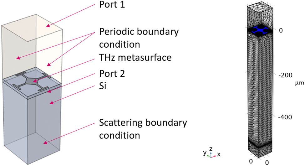
Schematic view of the numerical model (right) and mesh used (left).
4 THz metasurface fabrication and measurement
As assumed in the model, the microfabrication process was performed on a 520 µm thick low boron-doped silicon (Si) (100) wafer (specific resistivity, 10–20 Ω cm). Initially, the wafer was coated with a 170 nm thick wet thermal oxide layer (SiO2) on both sides at 1,000°C for 20 min using a Tempress furnace. Subsequently, the front side of the wafer was subjected to thermal evaporation of 500 nm aluminum in a Balzers vacuum evaporator. The wafer was then coated with an AZ 1505 photoresist layer (4,000 rpm, 2,500 rpm/s, and 25 s), and soft bake was performed at 100°C for 50 s. The photoresist was exposed by the designed mask using the contact/proximity printer Suess-MA6. Then, the wafer was developed in an AZ351B:H2O (1:5) solution for 60 s, providing a minimum feature size of about 1.5 µm. Subsequently, a hard bake process was carried out in an oven at 120°C for 10 min. The aluminum layer was wet-chemically structured with a phosphoric acid etching mixture at 43°C, and the photoresist layer was removed using oxygen plasma (1,000 W, 400 sccm O2). The influence of uncertainties in the manufacturing process on the quality of terahertz metasurfaces is described in detail in the study of Lopato et al. [19]. Finally, individual chips for measurement purposes were separated using a diamond saw. The manufacturing process flowchart is illustrated in Figure 6. Figure 7 shows the fabricated structure. Figure 7a shows a larger section of the matrix, while Figure 7b–e shows the outermost sections of the structure.

Microfabrication process flowchart.

Microscopy photo of the manufactured structure. (a) view of the larger part of the structure and (b–e) views of the outer sections of the structure.
The fabricated chips with the proposed metasurface were experimentally characterized for validation of the simulation results. The measurements were conducted using a TeraFlash smart terahertz time-domain spectroscopy (THz-TDS) system from Toptica, Germany, as depicted in Figure 8. The transmission setup was used, with transmission (Tx) and receiver (Rx) heads positioned on opposite sides of the examined metasurface. An electromagnetic pulse with terahertz frequency content was generated by a photoconductive antenna and directed toward the evaluated metasurface structure through a set of curved reflectors. After interacting with the metasurface, the modified THz pulses were defocused and propagated through another set of curved reflectors before being received by the photoconductive antenna. The focal point was 2D scanned over the entire metasurface in order to obtain the interaction with various geometries (various G and T values) of the structural elements. Both G and T parameters depend on (x, y) positions of a unit cell in the chip. It is not possible to measure the response (thus the resonant frequency) of a single element, the focal point of THz beam interacts with a few elements, which are relatively similar – the change in T and G is small for the distance comparable with a size of active part of focal point. This means that all the unit cells covered by the focal point have more or less the same resonant frequencies. The distributions of measured resonant frequencies were obtained by a raster scan for selected (x, y) positions. The focusing spot size (the area of incidence of the terahertz beam) was noticeably less than 1 mm in diameter. After acquisition of time domain signals using a TDS spectroscope (averaged from 1,000 single measurements), frequency domain amplitude responses were calculated using Fourier transform in the case of both signals transmitted through a metasurface containing a chip and a background signal (transmitted without the chip). The spectrum obtained with the chip was subtracted from the background spectrum. The resonant frequency was calculated as the frequency of the resonant curve minimum. The potential sources of errors in measuring resonant frequencies and resonant curves could be due to water absorption peaks (measurements were performed in open space without reduction of humidity or other gases in air), frequency-dependent absorption of silicon wafer, and the FP effect.

Photo of a THz-TDS measurement system.
5 Results
The developed numerical model was utilized to optimize the Jerusalem cross-based metasurface (obtain the geometry parameters) and conduct the analyses under consideration. The exemplary results obtained within the simulation are illustrated in Figures 9 and 10. The frequency response of transmission (|S 21|) and reflection (|S 11|) scattering matrix parameters for T = 30 µm and G = 30 µm are presented as an example in Figure 9. It is evident from the results that there is one resonance observed at f 1 = 0.72 THz. For this resonant frequency, the electric field distribution is shown in Figure 10. The same figure shows the distribution of normalized current density for various structural element shapes and three selected frequencies. The highest current densities correspond to frequencies for which resonance occurs for a given shape (defined by parameters G and T). This analysis shows which parts of the structural elements are responsible for a specific resonance. Additionally, frequency curves obtained in measurements for various combinations of G and T parameters are presented in Figure 9, showing variability of the resonant frequency.

Example characteristics of reflection S 11 and transmission S 21 coefficients obtained in simulations – resonance observed at f 1 = 0.72 THz (left side) and the S 21 coefficient obtained in measurements for various combinations of G and T parameters (right side).

Example results: electric field norm (V/m) for resonant frequency f 1 = 0.72 THz for T = 30 µm and G = 30 µm (left side) and distribution of the normalized (to a maximum value) electric current density in the case of various shapes of structural element and selected frequencies (right side).
As assumed, the modification of G and T parameters of cell geometry causes a variation of the resonant frequency f 1. This dependence is illustrated in Figures 11 and 12 in the case of numerical analysis (left) and measurement results (right). The increase of the T parameter value causes a decrease of the resonant frequency, while the increase of G influences in the opposite way, thus increasing the f 1. This relation is also presented in Figure 12 in a more convenient form. Good agreement between numerical and experimental results was achieved. The measured time domain signals were transformed to the frequency domain using the Fourier transform. Tunability range in the case of simulations was 0.80 and 0.79 THz for measurements. The achieved minimum and maximum frequencies were 0.44–1.24 THz for the simulations and 0.48–1.27 THz for the measurements. The quality factor Q obtained in the case of metasurfaces ranged from 2.76 obtained using fano resonance [34] to 3.5 using dipole resonance [35], 58 for fano resonance-BIC (bound states in the continuum) [36], and even 67.2 for quasi-BIC-based all-dielectric resonators [37]. In the case of the structure proposed in this work, the obtained Q factors are in the range of 5–7 for simulations and 2–3.5 for measurements. This structure with unit cell dimensions depending on the position in the chip will generally have a lower Q factor compared to fixed geometry metasurfaces. The active part of focal point interacts with many slightly different unit cells (G and T parameters are monotonic) that cause the blurring of the resonant curve and thus a decrease of the Q factor.

Dependence of the first resonant frequency, f 1, on the G and T parameters in the case of numerical analysis (left side) and measurement results (right side).

Dependence of the first resonant frequency, f 1, on the G and T parameters in the case of numerical analysis (left) and measurement results (right).
Dependence of the first resonant frequency on the G and T parameters was less smooth for the experimental results because the FP effect is not efficiently suppressed (influence of the silicon substrate resonator effect). A better FP effect reduction technique is necessary for the measurements.
G and T parameters were found to be linearly distributed over the metasurface chip (Figures 3 and 4). As shown in Figures 11 and 12, the resonant frequency is not linearly dependent on G and T parameter values. Considering the simplest resonator of rectangular shape or half-wavelength dipole antenna, the basic resonance (half wavelength per length l of the resonator; l = λ/2) occurs for f R = c/(2l), where c is the speed of light in air. This shows the nonlinear dependence between the length l of the resonator (or any resonating part of the metasurface cell like arms of the main cross of length L, side arms of length T, and square of the said length G) and the resonant frequency f R. If the application needs a linear dependence, the spatial distribution of G and T within the chip should be changed in a specific, nonlinear manner.
6 Conclusions
This article presents the concept of a tunable metasurface in which the geometry of a single cell depends on its position within the matrix. The structural element was built based on a Jerusalem cross subjected to some modifications: the length of the elements ending the arms of the cross and the size of the square built into the cross change according to the element position in the whole array. The metasurface built based on the proposed structural element is a resonance structure for the transmitted THz wave. Changing the geometry of this element causes the tuning of the resonant frequency within a certain frequency range (0.44–1.24 THz). This allows one to obtain tunable sensors – the resonant frequency depends on the position of the THz beam focal point. The change in T and G geometry parameters is linear in both orthogonal x and y directions, which causes the nonlinear change of resonant frequency. Application of a single parameter (only T or G) change is also possible, but a superposition of the influence of both parameters enables obtaining a wider resonant frequency tunability range.
The metasurfaces were realized using photolithography-based microtechnology and standard thin film techniques. The obtained novel structure with high tunability of the resonance frequency allowed examining changes in the properties of a thin dielectric layer (analyte) and a wide range of changes in the resonance frequency. This significantly increases the possibilities of identifying small amounts of substances or small changes in substance concentrations in thin films or liquid materials. This will be a goal of further research as well as reducing the size of the structure to shift toward shorter wavelengths (to increase the sensitivity to smaller material changes) and replacing part of the structural element geometry with a cantilever made of magnetic materials not anchored to the substrate, allowing additional reconfiguration using an external magnetic field. Generally, the THz metasurface sensors offer an accurate evaluation of micrometer-scale thin films, though they struggle with ultra-thin layers compared to optical and X-ray methods. THz metasurface sensors are highly sensitive to refractive index changes in thicker films, but ellipsometry and XRR (X-ray reflectometry) are more sensitive for ultra-thin layers (sub-nanometer films). Regarding the costs, THz metasurface solutions are more expensive than ellipsometry but potentially less expensive than XRR. Overall, THz metasurfaces are promising but currently still less effective for ultra-thin films than existing technologies, which opens up the field to new ideas and research.
Acknowledgements
We would like to thank Xenia Seng and Alexander Filbert from the Institute of Microsystems Technology, Furtwangen University, for carrying out the microfabrication process.
-
Funding information: This work was conducted within the project “RE-TERA- Reconfigurable terahertz devices for EM waves manipulation and sensing applications,” co-financed by the Polish National Agency for Academic Exchange (NAWA, Poland) and German Academic Exchange Service (DAAD, Germany) under grant no. PPN/BDE/2021/1/00012/U/00001, ID: 57602825, and partially funded by the National Science Centre (NCN, Poland) grant no. 2022/47/I/ST7/02055 and Deutsche Forschungsgmeinschaft (DFG, Germany), grant no. ME 2093/9-1, within the OPUS-24 (LAP) project “Investigation of electromagnetic properties of terahertz meta-surfaces tunable using multidirectional magnetic field.”
-
Author contributions: All authors have accepted responsibility for the entire content of this manuscript and consented to its submission to the journal, reviewed all the results, and approved the final version of the manuscript. PL designed, simulated, measured, and evaluated the metasurface. MH and GP wrote the main manuscript text, produced most included figures, and were involved in the measurements. UM and AK were responsible for the fabrication process development, fabrication of metasurface chips (and their evaluation), and description of the microfabrication process. PL was responsible for the concept of the article. PL and UM were responsible for funding acquisition. All authors reviewed the manuscript.
-
Conflict of interest: G.P., who is the co-author of this article, is a current Editorial Board member of Open Engineering. This fact did not affect the peer-review process. The authors declare no other conflict of interest.
-
Data availability statement: The data that support the findings of this study are available upon reasonable request from the authors.
References
[1] Torres-Huerta AL, Antonio-Pérez A, García-Huante Y, Alcázar-Ramírez NJ, Rueda-Silva JC. Biomolecule-based optical metamaterials: Design and applications. Biosensors. 2022;12:962.10.3390/bios12110962Search in Google Scholar PubMed PubMed Central
[2] Lopato P, Herbko M, Mescheder U, Kovacs A. Influence of a thin dielectric layer on resonance frequencies of square SRR metasurface operating in THz band. Open Eng. 2023;13:20220400.10.1515/eng-2022-0400Search in Google Scholar
[3] Susuzki T, Sekiya M, Sato T, Takebayashi Y. Negative refractive index metamaterial with high transmission, low reflection, and low loss in the terahertz waveband. Opt Express. 2018;26(7):8314–24.10.1364/OE.26.008314Search in Google Scholar PubMed
[4] Hindy MA, ElSagheer RM, Yassen MS. Experimental retrieval of the negative parameters “Permittivity and Permeability” based on a circular split ring resonator (CSRR) left handed metamaterial. J Electr Syst Inf Technol. 2018;5(2):208–15.10.1016/j.jesit.2017.05.004Search in Google Scholar
[5] Li A, Singh S, Sievenpiper D. Metasurfaces and their applications. Nanophotonics. 2018;7(6):989–1011.10.1515/nanoph-2017-0120Search in Google Scholar
[6] Alu A, Engheta N. Plasmonic and metamaterial cloaking: physical mechanisms and potentials. J Opt A: Pure Appl Opt. 2008;10(9):093002.10.1088/1464-4258/10/9/093002Search in Google Scholar
[7] Jing X, Feng D, Tian Y, Li M, Chu C, Li C, et al. Design of two invisibility cloaks using transmissive and reflective metamaterial-based multilayer frame microstructures. Opt Express. 2020;28(24):35528–39.10.1364/OE.409137Search in Google Scholar PubMed
[8] Haxha S, AbdelMalek F, Ouerghi F, Charlton MDB, Aggoun A, Fang X. Metamaterial superlenses operating at visible wavelength for imaging applications. Sci Rep. 2018;8:16119.10.1038/s41598-018-33572-ySearch in Google Scholar PubMed PubMed Central
[9] Wang Z, Yan B, Monks J, Yue L. All-dielectric metamaterial superlenses: A new route to near-perfect lenses. In Proceedings of 2017 Conference on Lasers and Electro-Optics Europe & European Quantum Electronics Conference (CLEO/Europe-EQEC); 25-29 June 2017. Munich, Germany; 2017.10.1109/CLEOE-EQEC.2017.8087123Search in Google Scholar
[10] Cui Y, Fung KH, Xu J, Ma H, Jin Y, He S, et al. Ultrabroadband light absorption by a sawtooth anisotropic metamaterial slab. Nano Lett. 2012;12(3):1443–7.10.1021/nl204118hSearch in Google Scholar PubMed
[11] Yang F, Li R-H, Tan S-L, Dong J-W, Jiang SJ. Visible-mid infrared ultra-broadband and wide-angle metamaterial perfect absorber based on cermet films with nano-cone structure. Nanophotonics. 2023;12(13):2451–60.10.1515/nanoph-2023-0021Search in Google Scholar PubMed PubMed Central
[12] Patel SK, Surve J, Katkar V, Parmar J. Machine learning assisted metamaterial-based reconfigurable antenna for low-cost portable electronic devices. Sci Rep. 2022;12:12354.10.1038/s41598-022-16678-2Search in Google Scholar PubMed PubMed Central
[13] Kaur P, Bansal S, Kumar N. SRR metamaterial-based broadband patch antenna for wireless communications. J Eng Appl Sci. 2022;69:47.10.1186/s44147-022-00103-6Search in Google Scholar
[14] Sbeah ZA, Adhikari R, Sorathiya V, Chauhan D, Chang SH, Dwivedi RP. A review on metamaterial sensors based on active plasmonic materials. Plasmonics. 2023;18:1619–38.10.1007/s11468-023-01904-ySearch in Google Scholar
[15] Islam MR, Islam MT, M. Salaheldeen M, Bais B, Almalki SHA, Alsaif H, et al. Metamaterial sensor based on rectangular enclosed adjacent triple circle split ring resonator with good quality factor for microwave sensing application. Sci Rep. 2022;12:6792.10.1038/s41598-022-10729-4Search in Google Scholar PubMed PubMed Central
[16] Zhou J, Zhang P, Han J, Li L, Huang Y. Metamaterials and metasurfaces for wireless power transfer and energy harvesting. Proc IEEE. 2022;110(1):31–55.10.1109/JPROC.2021.3127493Search in Google Scholar
[17] Nowak M. Metamaterial-based sub-microwave electromagnetic field energy harvesting system. Energies. 2021;14:3370.10.3390/en14123370Search in Google Scholar
[18] Hossain MB, Faruque MRI, Islam MT, Khandaker MU, Tamam N, Sulieman A. Modified coptic cross shaped split-ring resonator based negative permittivity metamaterial for quad band satellite applications with high effective medium ratio. Materials. 2022;15:3389.10.3390/ma15093389Search in Google Scholar PubMed PubMed Central
[19] Lopato P, Herbko M, Gora P, Mescheder U, Kovacs A, Filbert A. Numerical analysis of the influence of fabrication process uncertainty on terahertz metasurface quality. Electronics. 2023;12:2198.10.3390/electronics12102198Search in Google Scholar
[20] Charola S, Patel SK, Parmar J, Jadeja R. Multiband Jerusalem cross-shaped angle insensitive metasurface absorber for X-band application. J Electromagn Waves Appl. 2021;36(2):180–92.10.1080/09205071.2021.1960643Search in Google Scholar
[21] Fu X, Yang J, Wang J, Han Y, Ding C, Qiu T, et al. Completely spin-decoupled geometric phase of a metasurface. Photonics Res. 2023;11(7):1162–74.10.1364/PRJ.473698Search in Google Scholar
[22] Cong L, Xu N, Zhang W, Singh R. Polarization control in terahertz metasurfaces with the lowest order rotational symmetry. Adv Opt Mater. 2015;3(9):1176–83.10.1002/adom.201500100Search in Google Scholar
[23] Charipar N, Johns P, Suess RJ, Kim H, Geldmeier J, Trammell S, et al. Light tunable plasmonic metasurfaces. Opt Express. 2020;28(15):22891–8.10.1364/OE.396118Search in Google Scholar PubMed
[24] Zhang XG, Jiang WX, Jiang HL, Wang Q, Tian HW, Bai L, et al. An optically driven digital metasurface for programming electromagnetic functions. Nat Electron. 2020;3:165–71.10.1038/s41928-020-0380-5Search in Google Scholar
[25] Liu M, Hwang HY, Tao H, Strikwerda AC, Fan K, Keiser GR, et al. Terahertz-field-induced insulator-to-metal transition in vanadium dioxide metamaterial. Nature. 2012;487:345–8.10.1038/nature11231Search in Google Scholar PubMed
[26] Xu R, Lin YS. Flexible and controllable metadevice using self-assembly MEMS actuator. Nano Lett. 2021;21(7):3205–10.10.1021/acs.nanolett.1c00391Search in Google Scholar PubMed
[27] Ozbey B, Aktas O. Continuously tunable terahertz metamaterial employing magnetically actuated cantilevers. Opt Express. 2011;19(7):5741.10.1364/OE.19.005741Search in Google Scholar PubMed
[28] Chuang W-C, Lee H-L, Chang P-Z, Hu Y-C. Review on the modeling of electrostatic MEMS. Sensors. 2010;10:6149–71.10.3390/s100606149Search in Google Scholar PubMed PubMed Central
[29] Feng Y, Tsao H, Barker NS. THz MEMS switch design. Micromachines. 2022;13:745.10.3390/mi13050745Search in Google Scholar PubMed PubMed Central
[30] Pitchappa P, Manjappa M, Ho CP, Qian Y, Singh R, Singh N, et al. Active control of near-field coupling in conductively coupled microelectromechanical system metamaterial devices. Appl Phys Lett. 2016;108:111102.10.1063/1.4943974Search in Google Scholar
[31] Arezoomand AA, Zarrabi FB, Heydari S, Gandji NP. Independent polarization and multi-band THz absorber base on Jerusalem cross. Opt Commun. 2015;352:121–6.10.1016/j.optcom.2015.05.003Search in Google Scholar
[32] Fujii T, Ando A, Sakabe Y. Characterization of dielectric properties of oxide materials in frequency range from GHz to THz. J Eur Ceram Soc. 2006;26:1857–60.10.1016/j.jeurceramsoc.2005.09.094Search in Google Scholar
[33] Sun W-F, Wang X-K, Zhang Y. Measurement of refractive index for high reflectance materials with terahertz time domain reflection spectroscopy. Chin Phys Lett. 2009;26(11):114210.10.1088/0256-307X/26/11/114210Search in Google Scholar
[34] Chen M, Singh L, Xu N, Singh R, Zhang W, Xie L. Terahertz sensing of highly absorptive water-methanol mixtures with multiple resonances in metamaterials. Opt Express. 2017;25:14089.10.1364/OE.25.014089Search in Google Scholar PubMed
[35] Lin T, Zeng Q, Huang Y, Zhong S, Shi T, Zhong Y, et al. Substrate-free terahertz metamaterial sensors with customizable configuration and high performance. Adv Opt Mater. 2024;12(29):2400689.10.1002/adom.202400689Search in Google Scholar
[36] Liu B, Peng Y, Jin Z, Wu X, Gu H, Wei D, et al. Terahertz ultrasensitive biosensor based on wide-area and intense light-matter interaction supported by QBIC. Chem Eng J. 2023;462:142347.10.1016/j.cej.2023.142347Search in Google Scholar
[37] Lin T, Huang Y, Zhong S, Shi T, Sun F, Zhong Y, et al. Passive trapping of biomolecules in hotspots with all-dielectric terahertz metamaterials. Biosens Bioelectron 2024;251:116126.10.1016/j.bios.2024.116126Search in Google Scholar PubMed
© 2025 the author(s), published by De Gruyter
This work is licensed under the Creative Commons Attribution 4.0 International License.
Articles in the same Issue
- Research Articles
- Modification of polymers to synthesize thermo-salt-resistant stabilizers of drilling fluids
- Study of the electronic stopping power of proton in different materials according to the Bohr and Bethe theories
- AI-driven UAV system for autonomous vehicle tracking and license plate recognition
- Enhancement of the output power of a small horizontal axis wind turbine based on the optimization approach
- Design of a vertically stacked double Luneburg lens-based beam-scanning antenna at 60 GHz
- Synergistic effect of nano-silica, steel slag, and waste glass on the microstructure, electrical resistivity, and strength of ultra-high-performance concrete
- Expert evaluation of attachments (caps) for orthopaedic equipment dedicated to pedestrian road users
- Performance and rheological characteristics of hot mix asphalt modified with melamine nanopowder polymer
- Second-order design of GNSS networks with different constraints using particle swarm optimization and genetic algorithms
- Impact of including a slab effect into a 2D RC frame on the seismic fragility assessment: A comparative study
- Analytical and numerical analysis of heat transfer from radial extended surface
- Comprehensive investigation of corrosion resistance of magnesium–titanium, aluminum, and aluminum–vanadium alloys in dilute electrolytes under zero-applied potential conditions
- Performance analysis of a novel design of an engine piston for a single cylinder
- Modeling performance of different sustainable self-compacting concrete pavement types utilizing various sample geometries
- The behavior of minors and road safety – case study of Poland
- The role of universities in efforts to increase the added value of recycled bucket tooth products through product design methods
- Adopting activated carbons on the PET depolymerization for purifying r-TPA
- Urban transportation challenges: Analysis and the mitigation strategies for road accidents, noise pollution and environmental impacts
- Enhancing the wear resistance and coefficient of friction of composite marine journal bearings utilizing nano-WC particles
- Sustainable bio-nanocomposite from lignocellulose nanofibers and HDPE for knee biomechanics: A tribological and mechanical properties study
- Effects of staggered transverse zigzag baffles and Al2O3–Cu hybrid nanofluid flow in a channel on thermofluid flow characteristics
- Mathematical modelling of Darcy–Forchheimer MHD Williamson nanofluid flow above a stretching/shrinking surface with slip conditions
- Energy efficiency and length modification of stilling basins with variable Baffle and chute block designs: A case study of the Fewa hydroelectric project
- Renewable-integrated power conversion architecture for urban heavy rail systems using bidirectional VSC and MPPT-controlled PV arrays as an auxiliary power source
- Exploitation of landfill gas vs refuse-derived fuel with landfill gas for electrical power generation in Basrah City/South of Iraq
- Two-phase numerical simulations of motile microorganisms in a 3D non-Newtonian nanofluid flow induced by chemical processes
- Sustainable cocoon waste epoxy composite solutions: Novel approach based on the deformation model using finite element analysis to determine Poisson’s ratio
- Impact and abrasion behavior of roller compacted concrete reinforced with different types of fibers
- Architectural design and its impact on daylighting in Gayo highland traditional mosques
- Structural and functional enhancement of Ni–Ti–Cu shape memory alloys via combined powder metallurgy techniques
- Design of an operational matrix method based on Haar wavelets and evolutionary algorithm for time-fractional advection–diffusion equations
- Design and optimization of a modified straight-tapered Vivaldi antenna using ANN for GPR system
- Analysis of operations of the antiresonance vibration mill of a circular trajectory of chamber vibrations
- Functions of changes in the mechanical properties of reinforcing steel under corrosive conditions
- Enhanced PAPR reduction in NOMA systems using modified SLM and PTS techniques for power-efficient 5G and beyond networks
- Hybrid mechanics-informed machine learning models for predicting mechanical failure in graphene sponge: a low-data strategy for mechanical engineering applications
- Design of shafts of a two-piece chain conveyor as a part of a modification of a mobile working machine
- Review Articles
- A modified adhesion evaluation method between asphalt and aggregate based on a pull off test and image processing
- Architectural practice process and artificial intelligence – an evolving practice
- 10.1515/eng-2025-0148
- Special Issue: 51st KKBN - Part II
- The influence of storing mineral wool on its thermal conductivity in an open space
- Use of nondestructive test methods to determine the thickness and compressive strength of unilaterally accessible concrete components of building
- Use of modeling, BIM technology, and virtual reality in nondestructive testing and inventory, using the example of the Trzonolinowiec
- Tunable terahertz metasurface based on a modified Jerusalem cross for thin dielectric film evaluation
- Integration of SEM and acoustic emission methods in non-destructive evaluation of fiber–cement boards exposed to high temperatures
- Non-destructive method of characterizing nitrided layers in the 42CrMo4 steel using the amplitude-frequency technique of eddy currents
- Evaluation of braze welded joints using the ultrasonic method
- Analysis of the potential use of the passive magnetic method for detecting defects in welded joints made of X2CrNiMo17-12-2 steel
- Analysis of the possibility of applying a residual magnetic field for lack of fusion detection in welded joints of S235JR steel
- Eddy current methodology in the non-direct measurement of martensite during plastic deformation of SS316L
- Methodology for diagnosing hydraulic oil in production machines with the additional use of microfiltration
- Special Issue: IETAS 2024 - Part II
- Enhancing communication with elderly and stroke patients based on sign-gesture translation via audio-visual avatars
- Optimizing wireless charging for electric vehicles via a novel coil design and artificial intelligence techniques
- Evaluation of moisture damage for warm mix asphalt (WMA) containing reclaimed asphalt pavement (RAP)
- Comparative CFD case study on forced convection: Analysis of constant vs variable air properties in channel flow
- Evaluating sustainable indicators for urban street network: Al-Najaf network as a case study
- Node failure in self-organized sensor networks
- Comprehensive assessment of side friction impacts on urban traffic flow: A case study of Hilla City, Iraq
- Design a system to transfer alternating electric current using six channels of laser as an embedding and transmitting source
- Security and surveillance application in 3D modeling of a smart city: Kirkuk city as a case study
- Modified biochar derived from sewage sludge for purification of lead-contaminated water
- The future of space colonisation: Architectural considerations
- Design of a Tri-band Reconfigurable Antenna Using Metamaterials for IoT Applications
- Special Issue: AESMT-7 - Part II
- Experimental study on behavior of hybrid columns by using SIFCON under eccentric load
- Special Issue: ICESTA-2024 and ICCEEAS-2024
- A selective recovery of zinc and manganese from the spent primary battery black mass as zinc hydroxide and manganese carbonate
- Special Issue: REMO 2025 and BUDIN 2025
- Predictive modeling coupled with wireless sensor networks for sustainable marine ecosystem management using real-time remote monitoring of water quality
- Management strategies for refurbishment projects: A case study of an industrial heritage building
- Structural evaluation of historical masonry walls utilizing non-destructive techniques – Comprehensive analysis