In situ bow reduction during sublimation growth of cubic silicon carbide
-
Manuel Kollmuß
 ,
Marco Mauceri
,
Marco Mauceri

Abstract
Sublimation growth of cubic silicon carbide (3C–SiC) with diameters of 50 and 100 mm was performed on freestanding homoepitaxial grown seeds. For both seeds and sublimation grown crystals, two different relaxation axes with varying curvature could be observed with the higher bent axis aligned perpendicular to the original wafer flat. A general reduction in the wafer bow independent of the starting curvature and size of the seeds could be observed. Using the X-ray imaging, we could observe in situ that the bow reduction is linked to the growth of new material and cannot be initiated by heat up or cool down processes alone. Raman spectroscopy of the grown crystals revealed that the observed flattening goes along with a tensing of the seeding layers while the surface of the crystals remains free of a stress gradient. A slight concave bending of lattice planes along the main relaxation axis could be observed by high-resolution XRD rocking curve measurements while for the lower bent axis, no lattice plane bending occurred. Full width half maximum values of the (002) reflection showed values as low as 67 arcseconds proofing the possibility to grow large-area, high-quality 3C–SiC using sublimation growth.
1 Introduction
Silicon carbide (SiC) has gathered strong interest in industry and research for many years due to its extraordinary mechanical, optical, and electrical properties. The high breakdown voltage coupled with higher operation temperatures and high thermal conductivity makes it superior for power electronic applications with respect to silicon (Si) [1]. Currently, only the hexagonal polytypes, 4H and 6H, are commercially available. Due to recent progress with respect to the material quality [2], cubic SiC (3C–SiC) has been brought back into the focus of intense research. Compared to hexagonal SiC, the cubic polytype exhibits a smaller bandgap (2.39 eV), which can help to reduce the on-resistance of metal oxide semiconductor field effect transistors (MOSFET) in the range of 200–1,200 V [3]. Furthermore, the lowering of the conduction band minimum leads to a decreased density of states at the SiO2/3C–SiC interface, improving the channel mobility in MOSFETs [4]. In fact, the highest mobilities for an SiC-based MOSFET were reported by Uchida et al. [5] on the cubic polytype. 3C–SiC is also the only polytype that can be nucleated directly on Si using the heteroepitaxial chemical vapor deposition (CVD), potentially decreasing production costs due to the use of a cheaper starting material. A setback that comes with the use of Si is the lattice mismatch between 3C–SiC (4.36 Å) and Si (5.43 Å) as well as the difference in thermal expansion of up to approx. 25% (depending on the temperature) [6,7]. This results in stress that will induce extended and/or planar defects or can lead to wafer bending. Although it was possible to reduce both the wafer bow and defect density, the overall material quality of 3C–SiC is still not at the same level as for the hexagonal polytypes.
One promising approach to minimize the negative influence that comes from the heteroepitaxial growth by CVD was presented by Anzalone et al. [8]. After a first heteroepitaxial growth step on Si, the substrate is in situ molten inside the reactor and the remaining freestanding 3C layer is used as seed for consequent homoepitaxial CVD growth. Removal of the silicon will in this case eliminate the stress induced during cool down based on the different coefficients of thermal expansion. Such material can also be used as starting point for sublimation growth processes, especially the so-called close space physical vapor transport (CS-PVT). In the past, it was already presented that sublimation growth processes can help to decrease the stacking fault (SF) density [9] and the overall stress in the material [10] and reduce protrusion defects based on an overgrowth mechanism [11]. Moreover, using CS-PVT even the first large-scale bulk crystals (thickness ≥1 mm) could be realized on the mentioned homoepitaxial CVD seeds [12]. However, mechanical stability of the seeding layers remains a problem, which is strongly connected to wafer bowing.
In this work, we describe an in situ reduction of the mentioned wafer bows during CS-PVT growth. Stress analysis using the Raman spectroscopy was performed to observe the stress distribution and connect it to the remaining curvature of 50 and 100 mm freestanding 3C crystals. In addition, rocking curve (RC) measurements were used to determine effects of the unbending on the lattice planes and evaluate the overall crystalline quality of the grown material.
2 Materials and methods
All growth runs were conducted in an inductive heated state-of-the-art PVT reactor using two different hot zones for the growth of 50 and 100 mm crystals. The CS-PVT hot zones were designed with respect to the so-called sublimation sandwich consisting (from bottom to top) of a tantalum (Ta) foil, a solid SiC source wafer (mono- or polycrystalline), a graphite spacer, and a freestanding 3C–SiC seeding layer. The distance between source and seed was 1 mm for all growth runs. The Ta foil was introduced to ensure a silicon-rich gas phase beneficial for the stability of the cubic polytype. All source wafers were produced in our own labs using PVT. During growth runs, the temperature was controlled using optical pyrometers at the crucible top and bottom. The growth temperature was varied between 1,960 and 2,050°C at the crucible top and the pressure ranged between 5 × 10⁻³ and 3 mbar, resulting in growth rates of 50–200 µm·h−1. The gas ambient for all growth runs consisted of argon, the growth time was 4.5–8 h, and the thickness of the grown samples was 500-1,800 µm. In total, five crystals were grown, three in the 50 mm setup using a rectangular seeding layer (Crystals A–C) and two with the 100 mm setup using a round seeding layer (Crystals D and E). Due to the used graphite spacers, the resulting diameter of the grown crystals is slightly lower than the size of the used seeds. To prevent backside sublimation during the growth runs, a carbon containing backside coating was applied. For the growth of 50 mm diameter samples, the seeds were cut out of two larger wafers using laser ablation [13]. The two source wafers had a similar defect density and wafer bow, thus making the results highly comparable. All seeds were provided by LPE Epitaxial Technology Center in Catania and were grown using the CVD process mentioned in Section 1 (in detail also described in ref. [14]). The seeds were originally grown on an (001) oriented silicon substrate with an off-axis angle of 4°. After initial heteroepitaxy and Si melting, the thickness of 3C was increased to values between 200 and 400 µm.
For in situ visualization of the growth processes, a X-ray source and detector were located on opposite sides of the growth reactor. An X-ray tube operating at 70 kV and 7 mA acts as the source while an X-ray imaging plate was used as detector. The exposure time was set to 2.13 s and the visualization of the X-ray image was realized with a digital X-ray scanner. Wafer bow measurements were performed using a Zeta 300 profilometer with a 20× magnification. By focusing on the sample surface with a predefined pattern, the difference in z-direction between wafer center and edge could be obtained. To compensate for thickness variations over the samples, the thickness at each focus point was measured and accounted in the calculation of the wafer bow. The outermost area was excluded from the measurement to avoid distortion by rounding effects at the crystal edges. Raman spectroscopy was conducted on the surface of as-grown samples as well as on polished crosscuts of the crystals. A Horiba LabRAM HR Evolution confocal Raman microscope in backscattered geometry was used for the measurements, operating with a diode-pumped solid-state laser (laser power = 3.2 mW), a 50× magnification lens, and an optical grating of 1,800 g·mm−1. The laser wavelength was 532 nm, resulting in a penetration depth of approx. 300 µm based on the absorption coefficient of 3C–SiC. High-resolution X-ray diffraction (HRXRD) RC measurements were realized with a Seifert XRD 3003 PTS using a Cu X-ray tube, a multilayer mirror, and a Du–Mond Bartels monochromator. The monochromator consisting of two asymmetrical channel cut Ge (440) crystals ensures that only the CuKα1 radiation can pass [15]. The spot size on the sample for all measurements was 5.7 mm × 12.0 mm.
3 Results and discussion
Figure 1 shows the wafer bow measurement of a typical seeding layer for the growth of a 50 mm crystal. All used seeds had a convex-shaped bow when viewed from the original CVD growth side. As a consequence of the heteroepitaxial growth of the seeds on off-axis orientated Si, the symmetry of the cubic lattice is broken, resulting in two nonequivalent relaxation axes [16]. Consequently, also two different curvatures are visible along the direction parallel and perpendicular to the original wafer flat. We observed that the higher bent axis was perpendicular to the original wafer flat for all analyzed samples (seeds and grown crystals), which is in agreement with ref. [17]. The calculated curvatures along the two axes for the seed in Figure 1 are 0.06 and 7.24 m−1. After CS-PVT growth, the wafer bow for the crystal is reduced (Figure 1). Note that the outermost area was covered by the spacer during the growth (marked by the dashed line), resulting in the height difference between the sample center and the edges. Besides the overall reduced wafer bow, the difference in curvature along the two relaxation axes has been decreased during the sublimation growth. The corresponding curvatures are −0.30 and 1.02 m−1 after the growth run. The negative sign corresponds to a convex formed bending. The deflections at the lower edge can be attributed to agglomerations of protrusion defects, which will influence the focus point of the profilometer as well as the thickness measurement at this position.

Wafer bow measurement of a typical used seeding layer (left) and corresponding crystal after CS-PVT growth (right). For the seeding layer, two different relaxation axes – one vertical and the other horizontal – can be identified. After CS-PVT growth, the difference in curvature along the two axes as well as the overall wafer bow is decreased. The area inside the dashed line marks the area on which sublimation growth was conducted while the outer area was covered by the used graphite spacer.
A similar bow reduction could be observed for all growth runs independent of the sample size, growth temperature, or growth pressure. Figure 2 shows a 50 mm (Crystal A) and 100 mm (Crystal E) growth run in comparison. The curvature along the higher bent axis has a convex shape while along the other axis, only a small deviation in the vertical displacement can be seen. Although the overall vertical displacement for Crystal E is higher, the curvature of the two samples along the higher bent axis is approximately the same with −1.81 m−1 for Crystal A and −1.58 m−1 for Crystal E. Different to all other growth runs, Crystal E was grown on the former Si/3C–SiC interface side. In this case, the starting curvature is concave for the growth process. Independently, a reduction in the wafer bow could be realized during CS-PVT. The isotherms of the temperature field inside our used growth cells are flat by design. From the bulk SiC growth of hexagonal polytypes, it is already known that the growing crystals tend to adapt its form to the shape of the isotherms [18]. We assume that the same will happen during CS-PVT. Therefore, bow reduction should be possible for a free, non-fixed seeding layer independent of the starting curvature, which is consistent with our observations.
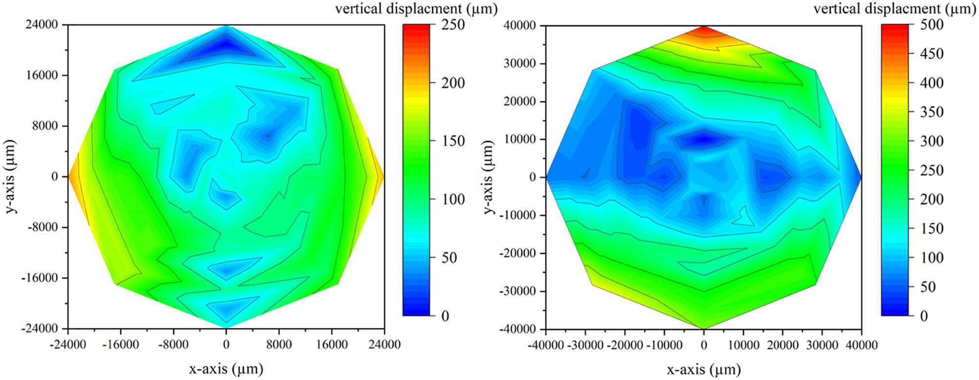
Comparison between a 50 mm (left, Crystal A) and a 100 mm (right, Crystal E) CS-PVT-grown 3C–SiC crystal. For both samples, two different curvatures along the two-relaxation axes can be seen. Although the starting curvature for the larger sample was concave, a reduction in the overall wafer bow could be realized.
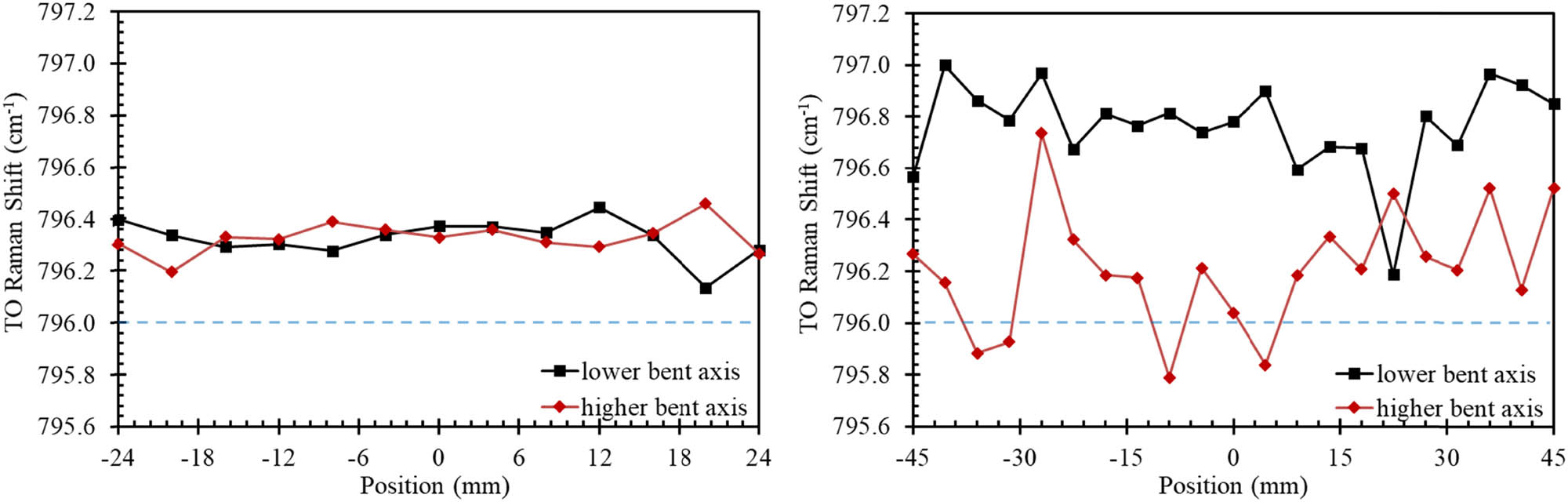
Figure 3 shows an image series taken during a 50 mm growth run using the X-ray imaging setup described in Section 2. The growth rate was chosen to be low (approx. 50 µm·h−1) to see even small changes that occur during the growth run. The seed was aligned in a way that the stronger bended axis was perpendicular to the radiation path of the X-ray source. The inserted seeding layer (215 µm thickness) had a clearly visible bow (Figure 3a), which does not disappear or decrease during the heat up of the reactor (Figure 3b). In a former work [12], we already discussed that the reduction in the wafer bow cannot be initiated by a temperature treatment alone but additional material growth is necessary. After 2 h, already a slight reduction in the curvature can be observed, revealing that the relaxation will start before the layer grown by CS-PVT has reached the thickness of the used seeding layer. This can be seen most easily at the edge of the seed in comparison to the non-deforming graphite spacer. During the remaining growth time, a further reduction in the wafer bow occurs (Figure 3c–e). At the growth end, the curvature has vanished in a way that the remaining bow could not be resolved with the used imaging setup (Figure 3e). During cool down of the system, no further effects could be observed. Curvature measurements revealed a value of approx. 1 m−1 for this growth run along the higher bowed relaxation axis compared to approx. 7 m−1 for the used seed.

In situ X-ray imaging of a 50 mm growth run (Crystal C). (a) Reference image after the hot zone was inserted in the growth setup, (b) after the growth temperature was reached, (c) after 2 h of growth, (d) after 4 h of growth, and (e) after 6 h of growth/at growth end. While no de-bending of the seed occurred during the heat up process, a reduction in the bow can be observed during the growth of additional material. The bow of the seed is also indicated by the transparent, dotted line. During the growth run, a bulging of the Ta foil occurred, resulting in a slight lift of the seeding stack on the right side, which does not influence the growth in a significant way.
Raman measurements were conducted on the surface along the two-relaxation axes of the grown crystals. For 3C–SiC, two typical peaks should appear during Raman spectroscopy: the transversal optical (TO) and the longitudinal optical (LO) phonon mode. In a perfect (001) orientated 3C–SiC crystal, the TO mode is prohibited by the selection rules [19]. However, due to misorientation, defects, and lattice distortions, this peak becomes visible. The TO mode is not affected by doping and, therefore, is well suited for the evaluation of stress present in the crystal. For a stress-free material, the peak is located at 796 cm−1 [20]. Tensile stress will shift the value toward lower Raman shifts while compressive stress will do the opposite. Figure 4 shows the results for the Raman surface measurements of Crystal A (50 mm diameter) and Crystal D (100 mm diameter). No significant stress gradient can be found along both relaxation axes. The overall strain is slightly compressive while the stress level appears to be increased for the larger sample. The higher fluctuating values for the 100 mm crystal can be associated with an increased thickness of the sample. The protrusion defects expand in size with increasing thickness and will lead to a higher surface roughness, potentially influencing the Raman signal.
Results of Raman measurements on the surface of Crystal A (50 mm) and Crystal D (100 mm) along the two relaxation axes of the crystal. The value for stress-free 3C–SiC is indicated by the dashed blue line. For both crystals no significant stress gradient can be observed for both measurement directions. The higher fluctuation of the 100 mm sample is attributed to the surface roughening by protrusion defects for increased crystal thickness compared to Crystal A.
Raman measurements can also be used to estimate the doping concentration of SiC based on the shift of the LO mode [21]. The crystals grown in this study were unintentionally doped with nitrogen and had doping levels between 1.0 and 4.5 × 1018 cm−3. The two sources of unintentional doping in the CS-PVT experiments are the released nitrogen from the used carbon isolations and the nitrogen incorporated in the SiC source wafers. While Calabretta et al. [22] reported that high nitrogen doping combined with growth on off-axis substrates could reduce the SF density in 3C–SiC for heteroepitaxial CVD, an increased wafer bow with increased nitrogen doping was reported in ref. [17]. Compared to literature, no significant influence of the nitrogen doping on the wafer bow could be observed in our study.
Figure 5 shows Raman line scans on the surface of a 50 mm sample grown with a special spacer. Thereby, a larger area of the seed was covered by the spacer allowing us to measure variations in the seeding layer before and after the growth run. The single scans were taken along vertical lines starting from the flat of the sample at five different lateral positions. Each scan included seven measurement spots and the value “zero” on the x-axis of the two graphs refers to the middle of the sample. The scheme of the measurement is also indicated by the inset in the left graph of Figure 5. For the line scans along the areas where growth has taken place (black and blue lines), no significant change with respect to the TO mode can be seen. However, for the covered area (red lines), a shift toward increased tensile stress can be observed after the growth run.
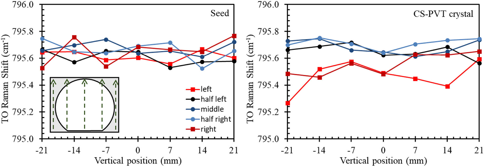
Results of Raman measurements on the surface before (left) and after (right) the CS-PVT growth. The scheme of the measurement procedure is indicated in the left-hand graph with the gray area covered by the spacer during the growth run. The values of the legend correspond to the lateral position of the line scan on the sample and the x-axis of the graphs indicates the measurement position within a line scan. For the uncovered area (black and blue lines), no significant change with regard to the TO mode can be seen while, for the covered area (red lines), a shift toward increased tensile stress is visible.
To further evaluate the stress distribution in the grown crystals, crosscuts were prepared out of two 50 mm diameter samples. For each sample, two different crosscuts were prepared: perpendicular to the higher bent axis and parallel to it. The results of the Raman measurements are displayed in Figure 6. For the crosscuts, a slight gradient toward tensile stress can be seen inside the seeding layer for the cut perpendicular to the higher bent relaxation axis. Once the interface between the seed and the CS-PVT grown crystal is reached, the stress values stay mostly constant. The position of the interface between seed and crystal is marked with a dashed line. In the crosscuts along the higher bent axis, a decreased stress gradient inside the seeding layer can be observed for Crystal A, while for Crystal B, no gradient is visible. In addition, for Crystal A, the overall compressive stress is slightly increased.

Results of Raman measurements for crosscuts of Crystals A and B. The orientation with respect to the higher bent axis of the samples is indicated in the upper right corner of the single scans. The interface between seed and PVT grown crystal is indicated by the dashed red line. For both samples, a gradient toward tensile stress inside the seeding layer is visible perpendicular to the higher bent axis while the stress stays fairly constant once the interface is reached. For the parallel cuts, this effect is reduced (Crystal A) or not visible at all (Crystal B).
The deformation of material will always go along with the releasing or introduction of stress and the movement of defects such as dislocations. In our case, the seeding layers are bent but also show low stress values. The flattening of the material should therefore induce stress into the material. Raman measurements of the TO-mode on the surface of our grown crystals displayed no significant stress overall. In addition, no stress gradient was visible along the two relaxation axes in the grown material. Crosscuts as well as the measurements depicted in Figure 5 revealed that the seeding layers are tensile stressed after the sublimation growth. Based on the bending direction, the flattening mechanism should result in compressive stress at the sample surface. Therefore, we conclude that the stress generated during the sublimation growth by the reduction of the bow will be mainly released by a tensing of the seeding layer. At this point, we cannot certainly exclude that defect generation will play an additional role in the bow relaxation during sublimation growth. However, based on the low full width half maximum (FWHM) values of RC measurements (Figure 7) and the fact that sublimation growth has already shown to reduce the SF density in 3C–SiC [9], we assume that defect generation will not be the significant mechanism for the flattening observed.
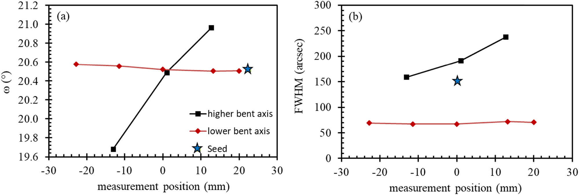
Results of HRXRD RC measurements of Crystal C. (a) Peak position of the (002) reflex. For the scan direction along the lower bent axis, no shift of the peak position can be seen. For the higher bent axis, a shift occurs corresponding to a concave bending of the lattice planes compared to the sample surface. The star marks the value measured on the seed after CS-PVT growth (the area was covered by the spacer during growth). (b) FWHM of the measured (002) peak. For the lower bent axis, low values were measured while the higher bent axis shows an increased FWHM. The value for the seed is again indicated by the star.
On the sample shown in Figure 5, additional HRXRD RC measurements were taken of the (002) reflex (Figure 7). If the lattice planes are bended or misaligned, a shift of the peak can be observed. In addition, the FWHM can be used to evaluate the quality of the grown material. Defects and other distortions of the lattice structure will lead to a broadening of the peak. The measurements were taken along the two-relaxation axes of the crystal and one spot of the seeding layer, which was covered by the graphite spacer. For the lower bent axis, the peak position is near the theoretical value and no considerable peak shift is visible along the scan direction. Furthermore, the average FWHM of the peaks is low with 69.10 ± 1.83 arcseconds. For the higher bent axis, a shift of the peak position is visible along the scan direction. In addition, peak splitting could be observed and the FWHM is increased with 190.63 ± 29.53 arcseconds. For the measurement spot on the seeding layer, the peak position is in line with the values of the lower bent axis. However, peak splitting could be observed and the FWHM is comparable to the values of the higher bent axis (153.09 arcseconds.).
Assuming horizontal aligned planes for the used seeding layers, a reduction in the bow during CS-PVT should bend the lattice planes at the sample edges. Although the surface of the sample appears flat, after the sublimation growth, the lattice planes are concave shaped for the higher bent axis with respect to the surface. Therefore, constructive interference according to Bragg´s law will be shifted toward lower values on one side of the analyzed sample and toward higher values on the opposite side. For the lower bent axis, no such shift could be observed. In addition, values of the FWHM as low as 67 arcseconds could be measured showing a high crystalline quality. As far as we know these are one of the lowest values reported for 3C–SiC in the literature. Due to the lower starting curvature on this axis, the bending of the lattice planes will be far less pronounced resulting in the high crystalline quality observed. Note that a shift of the peak position during RC measurements could also be linked to stress in the material. However, based on the results of the Raman measurements, the influence of stress on the peak position can be virtually neglected.
As expected, the peak position in the middle of the sample is the same for both scan directions of the RC measurements. However, for the higher bent axis, peak splitting could be observed for all measurement points. Zimbone et al. have shown that extended defects like SFs and inverted domain boundaries (IDBs) will prolong preferable along the [110] and [112] directions in (001) orientated 3C–SiC [23]. Similar preferential alignment of defects could explain why peak splitting only appears along the scan axis perpendicular to the original wafer flat during RC measurements. Shibahara et al. [24] reported that for the growth of 3C–SiC on off-axis, Si IDBs could be eliminated. The used seeding layers in this study were also prepared starting from an 4° off-axis Si substrate suggesting that the IDB density in the grown material is not sufficient enough to interfere with the RC measurements. However, for the growth of 3C–SiC with an off-cut toward the [110] direction, the SFs will align preferably along the (111) plane while prolongation of SFs along the (−1−11) plane will be suppressed [25]. Based on the expected alignment of SFs in our crystals, the density of defects should be increased for the direction perpendicular to the original wafer flat (higher bent axis) possibly interfering with the RC measurements.
4 Conclusions
We showed that CS-PVT can be used to the decrease the bow of 3C–SiC grown by homoepitaxial CVD. X-ray imaging enabled the in situ observation of the bow reduction during the growth runs and revealed that the flattening only occurs during growth but not during the heat up and cool down of the system. Raman measurements revealed no stress gradient and overall low stress levels on the surface of grown crystals while measurements on crosscuts showed tensile stress inside the seeding layers after the CS-PVT. We therefore assume that the stress induced into the material that accompanies the plastic deformation during the observed sample flattening is released by a tension induced into the seeding layer. HRXRD RC measurements showed a slight concave bending of the lattice planes along the higher bent relaxation axis but also confirmed the growth of high-quality material based on low FWHM of the (002) peak.
Acknowledgments
The funding by the European H2020 framework program for research and innovation under grant agreement numbers 720827 (CHALLENGE) and 899679 (SiComb) is greatly acknowledged. The authors would also like to thank Dr. Mathias Rommel and Mr. Leander Baier from the Fraunhofer IISB Institute for the possibility to use the Zeta 300 profilometer for bow measurements. We acknowledge financial support by Deutsche Forschungsgemeinschaft and Friedrich-Alexander-Universität Erlangen-Nürnberg within the funding programme “Open Access Publication Funding”.
-
Funding information: This work is partly funded by the European H2020 framework program for research and innovation under grant agreement numbers 720827 (CHALLENGE) and 899679 (SiComb).
-
Author contributions: Conceptualization: M.K. and P.J.W; methodology: M.K. and P.J.W.; formal analysis: M.K. and M.R.; investigation: M.K., P.J.W., and M.R.; resources: M.M., M.R., and F.L.V.; writing – original draft preparation: M.K.; writing – review and editing: M.K., M.M., M.R., F.L.V., and P.J.W.; visualization: M.K.; supervision: F.L.V and P.J.W; project administration: F.L.V. and P.J.W.; funding acquisition: F.L.V. and P.J.W; All authors have read and agreed to the published version of the article.
-
Conflict of interest: The authors state no conflict of interest.
-
Data availability statement: The datasets generated during and/or analyzed during the current study are available from the corresponding author on reasonable request.
References
[1] Wellmann, P. J. Review of SiC crystal growth technology. Semiconductor Science and Technology, Vol. 3310, 2018, id. 103001.10.1088/1361-6641/aad831Search in Google Scholar
[2] La Via, F., M. Zimbone, C. Bongiorno, A. La Magna, G. Fisicaro, I. Deretzis, et al. New approaches and understandings in the growth of cubic silicon carbide. Materials, Vol. 1418, 2021, id. 5348.10.3390/ma14185348Search in Google Scholar PubMed PubMed Central
[3] Van Zeghbroeck, B. H. F. Comparison of 3C–SiC and 4H-SiC Power MOSFETs. Proceedings of the 17th International Conference on Silicon Carbide and Related Materials, September, 17–22, 2017, Washington D.C., 2018, pp. 774–777.10.4028/www.scientific.net/MSF.924.774Search in Google Scholar
[4] Schöner, A., M. Krieger, G. Pensl, M. Abe, and H. Nagasawa. Fabrication and characterization of 3C‐SiC‐based MOSFETs. Chemical Vapor Deposition, Vol. 12, No. 8–9, 2006, pp. 523–530.10.1002/cvde.200606467Search in Google Scholar
[5] Uchida, H., A. Minami, T. Sakata, H. Nagasawa, and M. Kobayashi. High temperature performance of 3C–SiC MOSFETs with high channel mobility. Proceedings of the 14th International Conference on Silicon Carbide and Related Materials, September 11–16, 2011, Cleveland, 2012, pp. 1109–1112.10.4028/www.scientific.net/MSF.717-720.1109Search in Google Scholar
[6] Zielinski, M., S. Ndiaye, T. Chassagne, S. Juillaguet, R. Lewandowska, M. Portail, et al. Strain and wafer curvature of 3C‐SiC films on silicon: influence of the growth conditions. Physica status solidi (a), Vol. 204, No. 4, 2007, pp. 981–986.10.1002/pssa.200674130Search in Google Scholar
[7] Cimalla, V., J. Pezoldt, and O. Ambacher. Group III nitride and SiC based MEMS and NEMS: materials properties, technology and applications. Journal of Physics D: Applied Physics, Vol. 4020, 2007, id. 6386.10.1088/0022-3727/40/20/S19Search in Google Scholar
[8] Anzalone, R., M. Zimbone, C. Calabretta, M. Mauceri, A. Alberti, R. Reitano, et al. Temperature investigation on 3C–SiC homo-epitaxy on four-inch wafers. Materials, Vol. 1220, 2019, id. 3293.10.3390/ma12203293Search in Google Scholar PubMed PubMed Central
[9] Schuh, P., M. Schöler, M. Wilhelm, M. Syväjärvi, G. Litrico, and F. La Via, et al. Sublimation growth of bulk 3C–SiC using 3C–SiC-on-Si (1 0 0) seeding layers. Journal of Crystal Growth, Vol. 478, 2017, pp. 159–162.10.1016/j.jcrysgro.2017.09.002Search in Google Scholar
[10] Schuh, P., F. La Via, M. Mauceri, M. Zielinski, and P. J. Wellmann. Growth of large-area, stress-free, and bulk-like 3C–SiC (100) using 3C–SiC-on-Si in vapor phase Growth. Materials, Vol. 1213, 2019, id. 2179.10.3390/ma12132179Search in Google Scholar PubMed PubMed Central
[11] Schöler, M., F. La Via, M. Mauceri, and P. Wellmann. Overgrowth of protrusion defects during sublimation growth of cubic silicon carbide using free-standing cubic silicon carbide substrates. Crystal growth & design, 2021, Vol. 21, pp. 4046–4054.10.1021/acs.cgd.1c00343Search in Google Scholar
[12] Kollmuss, M., M. Schöler, R. Anzalone, M. Mauceri, F. La Via, P. J. Wellmann. Large area growth of cubic silicon carbide using close space PVT by application of homoepitaxial seeding. Proceedings of the 13th European Conference on Silicon Carbide and Related Materials, October 24–28, 2021, Tours, 2022, pp. 74–78.10.4028/p-6ef373Search in Google Scholar
[13] Zoppel, S., M. Farsari, R. Merz, J. Zehetner, G. Stangl, G. A. Reider, et al. Laser micro machining of 3C–SiC single crystals. Microelectronic Engineering, Vol. 83, No. 4–9, 2006, pp. 1400–1402.10.1016/j.mee.2006.01.064Search in Google Scholar
[14] Anzalone, R., N. Frazzeto, and F. La Via. Apparatus for growing a semiconductor wafer and associated manufacturing process. US 2021/0062361 A1, 2021.Search in Google Scholar
[15] Bartels, W. Characterization of thin layers on perfect crystals with a multipurpose high resolution x-ray diffractometer. Journal of Vacuum Science & Technology B: Microelectronics Processing and Phenomena, Vol. 1, No. 2, 1983, pp. 338–345.10.1116/1.582553Search in Google Scholar
[16] Zielinski, M., M. Portail, S. Roy, S. Kret, T. Chassagne, M. Nemoz, et al. Role of substrate misorientation in relaxation of 3C–SiC layers on Silicon. Proceedings of the 7th European Conference on Silicon Carbide and Related Materials, September 7–11, 2008, Barcelona, 2009, pp. 169–172.10.4028/www.scientific.net/MSF.615-617.169Search in Google Scholar
[17] La Via, F., M. Mauceri, V. Scuderi, C. Calabretta, M. Zimbone, and R. Anzalone. 3C–SiC bulk growth: Effect of growth rate and doping on defects and stress. Proceedings of the 18th International Conference on Silicon Carbide and Related Materials, September 29–October 4, 2019, Kyoto, 2020, pp. 120–125.10.4028/www.scientific.net/MSF.1004.120Search in Google Scholar
[18] Arzig, M., J. Steiner, M. Salamon, N. Uhlmann, and P. J. Wellmann. Influence of morphological changes in a source material on the growth interface of 4H-SiC single crystals. Materials, Vol. 1216, 2019, id. 2591.10.3390/ma12162591Search in Google Scholar PubMed PubMed Central
[19] Nakashima, S. H. H. Raman investigation of SiC polytypes. Physica Status Solidi (a), Vol. 162, No. 1, 1997, pp. 39–64.10.1002/1521-396X(199707)162:1<39::AID-PSSA39>3.0.CO;2-LSearch in Google Scholar
[20] Severino, A., C. Bongiorno, N. Piluso, M. Italia, M. Camarda, M. Mauceri, et al. High-quality 6 inch (111) 3C–SiC films grown on off-axis (111) Si substrates. Thin Solid Films, Vol. 518, No. 6, 2010, pp. 165–169.10.1016/j.tsf.2009.10.080Search in Google Scholar
[21] Yugami, H., S. Nakashima, A. Mitsuishi, A. Uemoto, M. Shigeta, K. Furukawa, et al. Characterization of the free‐carrier concentrations in doped β-SiC crystals by Raman scattering. Journal of applied physics, Vol. 61, No. 1, 1987, pp. 354–358.10.1063/1.338830Search in Google Scholar
[22] Calabretta, C., V. Scuderi, R. Anzalone, M. Mauceri, D. Crippa, A. Cannizzaro, et al. Effect of nitrogen and aluminum doping on 3C–SiC heteroepitaxial layers grown on 4 off-axis Si (100). Materials, Vol. 1416, 2021, id. 4400.10.3390/ma14164400Search in Google Scholar PubMed PubMed Central
[23] Zimbone, M., A. Sarikov, C. Bongiorno, A. Marzegalli, V. Scuderi, C. Calabretta, et al. Extended defects in 3C–SiC: Stacking faults, threading partial dislocations, and inverted domain boundaries. Acta Materialia, Vol. 213, 2021, id. 116915.10.1016/j.actamat.2021.116915Search in Google Scholar
[24] Shibahara, K., S. Nishino, and H. Matsunami. Antiphase-domain-free growth of cubic SiC on Si (100). Applied Physics Letters, Vol. 5026, 1987, pp. 1888–1890.10.1063/1.97676Search in Google Scholar
[25] Severino, A., M. Camarda, G. Condorelli, L. Perdicaro, R. Anzalone, M. Mauceri, et al. Effect of the miscut direction in (111) 3 C-Si C film growth on off-axis (111) Si. Applied physics letters, Vol. 9410, 2009, id. 101907.10.1063/1.3085769Search in Google Scholar
© 2022 the author(s), published by De Gruyter
This work is licensed under the Creative Commons Attribution 4.0 International License.
Articles in the same Issue
- Review Articles
- State of the art, challenges, and emerging trends: Geopolymer composite reinforced by dispersed steel fibers
- A review on the properties of concrete reinforced with recycled steel fiber from waste tires
- Copper ternary oxides as photocathodes for solar-driven CO2 reduction
- Properties of fresh and hardened self-compacting concrete incorporating rice husk ash: A review
- Basic mechanical and fatigue properties of rubber materials and components for railway vehicles: A literature survey
- Research progress on durability of marine concrete under the combined action of Cl− erosion, carbonation, and dry–wet cycles
- Delivery systems in nanocosmeceuticals
- Study on the preparation process and sintering performance of doped nano-silver paste
- Analysis of the interactions between nonoxide reinforcements and Al–Si–Cu–Mg matrices
- Research Articles
- Study on the influence of structural form and parameters on vibration characteristics of typical ship structures
- Deterioration characteristics of recycled aggregate concrete subjected to coupling effect with salt and frost
- Novel approach to improve shale stability using super-amphiphobic nanoscale materials in water-based drilling fluids and its field application
- Research on the low-frequency multiline spectrum vibration control of offshore platforms
- Multiple wide band gaps in a convex-like holey phononic crystal strip
- Response analysis and optimization of the air spring with epistemic uncertainties
- Molecular dynamics of C–S–H production in graphene oxide environment
- Residual stress relief mechanisms of 2219 Al–Cu alloy by thermal stress relief method
- Characteristics and microstructures of the GFRP waste powder/GGBS-based geopolymer paste and concrete
- Development and performance evaluation of a novel environmentally friendly adsorbent for waste water-based drilling fluids
- Determination of shear stresses in the measurement area of a modified wood sample
- Influence of ettringite on the crack self-repairing of cement-based materials in a hydraulic environment
- Multiple load recognition and fatigue assessment on longitudinal stop of railway freight car
- Synthesis and characterization of nano-SiO2@octadecylbisimidazoline quaternary ammonium salt used as acidizing corrosion inhibitor
- Perforated steel for realizing extraordinary ductility under compression: Testing and finite element modeling
- The influence of oiled fiber, freeze-thawing cycle, and sulfate attack on strain hardening cement-based composites
- Perforated steel block of realizing large ductility under compression: Parametric study and stress–strain modeling
- Study on dynamic viscoelastic constitutive model of nonwater reacted polyurethane grouting materials based on DMA
- Mechanical behavior and mechanism investigation on the optimized and novel bio-inspired nonpneumatic composite tires
- Effect of cooling rate on the microstructure and thermal expansion properties of Al–Mn–Fe alloy
- Research on process optimization and rapid prediction method of thermal vibration stress relief for 2219 aluminum alloy rings
- Failure prevention of seafloor composite pipelines using enhanced strain-based design
- Deterioration of concrete under the coupling action of freeze–thaw cycles and salt solution erosion
- Creep rupture behavior of 2.25Cr1Mo0.25V steel and weld for hydrogenation reactors under different stress levels
- Statistical damage constitutive model for the two-component foaming polymer grouting material
- Nano-structural and nano-constraint behavior of mortar containing silica aggregates
- Influence of recycled clay brick aggregate on the mechanical properties of concrete
- Effect of LDH on the dissolution and adsorption behaviors of sulfate in Portland cement early hydration process
- Comparison of properties of colorless and transparent polyimide films using various diamine monomers
- Study in the parameter influence on underwater acoustic radiation characteristics of cylindrical shells
- Experimental study on basic mechanical properties of recycled steel fiber reinforced concrete
- Dynamic characteristic analysis of acoustic black hole in typical raft structure
- A semi-analytical method for dynamic analysis of a rectangular plate with general boundary conditions based on FSDT
- Research on modification of mechanical properties of recycled aggregate concrete by replacing sand with graphite tailings
- Dynamic response of Voronoi structures with gradient perpendicular to the impact direction
- Deposition mechanisms and characteristics of nano-modified multimodal Cr3C2–NiCr coatings sprayed by HVOF
- Effect of excitation type on vibration characteristics of typical ship grillage structure
- Study on the nanoscale mechanical properties of graphene oxide–enhanced shear resisting cement
- Experimental investigation on static compressive toughness of steel fiber rubber concrete
- Study on the stress field concentration at the tip of elliptical cracks
- Corrosion resistance of 6061-T6 aluminium alloy and its feasibility of near-surface reinforcements in concrete structure
- Effect of the synthesis method on the MnCo2O4 towards the photocatalytic production of H2
- Experimental study of the shear strength criterion of rock structural plane based on three-dimensional surface description
- Evaluation of wear and corrosion properties of FSWed aluminum alloy plates of AA2020-T4 with heat treatment under different aging periods
- Thermal–mechanical coupling deformation difference analysis for the flexspline of a harmonic drive
- Frost resistance of fiber-reinforced self-compacting recycled concrete
- High-temperature treated TiO2 modified with 3-aminopropyltriethoxysilane as photoactive nanomaterials
- Effect of nano Al2O3 particles on the mechanical and wear properties of Al/Al2O3 composites manufactured via ARB
- Co3O4 nanoparticles embedded in electrospun carbon nanofibers as free-standing nanocomposite electrodes as highly sensitive enzyme-free glucose biosensors
- Effect of freeze–thaw cycles on deformation properties of deep foundation pit supported by pile-anchor in Harbin
- Temperature-porosity-dependent elastic modulus model for metallic materials
- Effect of diffusion on interfacial properties of polyurethane-modified asphalt–aggregate using molecular dynamic simulation
- Experimental study on comprehensive improvement of shear strength and erosion resistance of yellow mud in Qiang Village
- A novel method for low-cost and rapid preparation of nanoporous phenolic aerogels and its performance regulation mechanism
- In situ bow reduction during sublimation growth of cubic silicon carbide
- Adhesion behaviour of 3D printed polyamide–carbon fibre composite filament
- An experimental investigation and machine learning-based prediction for seismic performance of steel tubular column filled with recycled aggregate concrete
- Effects of rare earth metals on microstructure, mechanical properties, and pitting corrosion of 27% Cr hyper duplex stainless steel
- Application research of acoustic black hole in floating raft vibration isolation system
- Multi-objective parametric optimization on the EDM machining of hybrid SiCp/Grp/aluminum nanocomposites using Non-dominating Sorting Genetic Algorithm (NSGA-II): Fabrication and microstructural characterizations
- Estimating of cutting force and surface roughness in turning of GFRP composites with different orientation angles using artificial neural network
- Displacement recovery and energy dissipation of crimped NiTi SMA fibers during cyclic pullout tests