FPGA based telecommand system for balloon-borne scientific payloads
-
Anand Devarajan
 ,
Kapardhi Bangaru
,
Kapardhi Bangaru

Abstract
Telecommand (TC) plays a crucial role in the success of high-altitude balloon experiments. Bose, Ray-Chaudhuri, Hocquenghem (BCH) codes are commonly employed to ensure reliable command operation. The Balloon Facility (BF) of Tata Institute of Fundamental Research (TIFR) uses a TC system based on BCH (31,16) coding technique, to control balloon and payload operations. This paper presents prototyping and implementation of TC encoder and decoder using Spartan 6 Field Programmable Gate Array (FPGA). The code is written in Very high-speed integrated circuit Hardware Description Language (VHDL). Simulation and synthesis are done using Xilinx ISE 14.7 design suite. Simulation results show the design is robust. The TC encoder is implemented in a commercial FPGA development board and the TC decoder is implemented in a specially designed FPGA board, successfully. This paper presents the salient features of the TC system in use and the implementation of the system using FPGA.
1 Introduction
TIFR has been launching Zero-Pressure plastic balloons (from its launch base at BF, Hyderabad) that carry scientific payload up to stratospheric altitudes for research in astronomy, atmospheric science, astrobiology and space technology development (Anand, Suneel Kumar, and Ojha 2021). The balloon payload operations use TC uplink and telemetry downlink similar to spacecraft missions (Lin and Costello 1983; Prasad and Pal 2003). TC essentially is a message from the ground station to the balloon payload that is used to control its activities. Some of the operations performed by the TC system include orientation of on-board telescope for astronomical observations, sample air at different altitudes for atmospheric science studies, deploy booms after launch once the balloon is stable, switch on/off sub-systems, ballast release to control balloon ascent rate, firing pyro-cutters for balloon payload detachment once the mission is over (Anand, Suneel Kumar, and Ojha 2021; Gosh and Tandon 1982). BCH coding technique is commonly employed in the telecommand system used in spacecraft and balloon missions (Bansiya 1987; Gosh and Tandon 1982; Kasturirangan et al. 1993; Prasad and Pal 2003). Since late eighties, TIFR has been using the BCH (31,16) based TC system designed and implemented successfully in the APPLE satellite, by the Indian Space Research Organization (ISRO) (Bansiya 1987). The Telecommand Encoder (TE) was implemented using a Microprocessor and discrete Integrated Circuits (ICs) and the Telecommand Decoder (TD) too was implemented using discrete ICs populated on several printed circuit boards. Later TIFR implemented the TE and TD using multi-layer printed circuit boards and surface mount devices. With the increasing demand to lessen the size, weight along with power consumption particularly in the on-board TD, these have now been implemented using FPGA. This paper discusses the FPGA implementation of TE and TD. The paper is organized as follows. Section 2 discusses the features of the prevailing telecommand system. Section 3 deals with the FPGA implementation of the TE and TD with both hardware and software description. In Section 4, simulations results are presented with description. Section 5 comprises concluding remarks and future plans to improve the design further.
2 Telecommand system
2.1 BCH codes
A BCH code is a cyclic block code typically specified with respect to its generator polynomial. A cyclic code is a block code in which the circular shifts of every codeword provide another word that belongs to the code. Several single-bit codes from a similar polynomial are merged basically by the BCH into a single-producing polynomial with predictable distance properties along with the capability of rectifying numerous bit errors. For any positive integer m ≥ 3 and t < 2 m−1 there exists a binary BCH code (n, k) where codeword length n = 2 m − 1; parity check bits (n − k) is ≤mt; minimum distance d ≥ 2t + 1; it can correct t errors and can detect up to d − 1 errors. A more detailed math can be found in the literature (Lin and Costello 1983; Wallace 2001) and several others. Our telecommand system based on a binary BCH (31,16), has 15 parity check bits. The generator polynomial g(x) derived is x 15 + x 11 + x 10 + x 9 + x 8 + x 7 + x 5 + x 3 + x 2 + x + 1 and the parity check polynomial h(x) worked out is x16 + x 12 + x 11 + x 10 + x 9 + x 4 + x + 1 (Bansiya 1987; Wallace 2001).
2.2 Functional description of the telecommand system
The basic command word consists of 16 bits containing the information regarding the sync, decoder address, type of command and the actual 8 bit data for line selection in the case of ON/OFF command or the data to be transferred to on-board subsystems in the case of DATA command. It may be noted that sync and TD address are important to ensure that the command is directed at the intended spacecraft, in this case, the balloon payload. This also helps in breaking the cyclic property of BCH codes. The breaking of the cyclic property is needed since a cyclic shift results in another valid command which is not acceptable in our case (Bansiya 1987; Gosh and Tandon 1982). Thus, spurious command execution can be avoided. An internal board and the ground control station are the two components of the monitoring and telecommand system. The telecommand system can decode both information and pulse commands. A PC-based signal generator is employed at the ground control station to create the PCM coding signals in accordance with the effectual needs of the sensor, maintenance, and ballooning operation, with command selection being driven by a selection. Additional frequency shift keying (FSK) is used with a tone for zero-state along with 6.25 kHz for one state in the instruction sequence. Finally, this PCM–FSK modifies the carrier with FM. For the payloads to be removed from the navigation plane, the command functionality during flying is crucial, and the current system provides 100 % consistency and no error operation. The commands to the balloon payload are real-time operations as the balloon is always in line-of sight throughout the mission (except for long duration balloon flights) (Anand, Suneel Kumar, and Ojha 2021). Therefore, only an error detection scheme is employed in the telecommand system to reduce the possibility of commands getting decoded incorrectly due to transmission errors. BCH code is used in the error-detecting code to provide efficient, dependable, and error-free execution. The BCH codes are a category of error-correcting codes with straightforward construction and rigorous mathematical syntax. Due to the codes’ potent error-correcting capabilities, they are commonly utilized in data transfer. One of the vital characteristics of BCH codes is that the amount of symbol errors that the code can fix may be exactly regulated during code generation. Fifteen parity bits are generated from the 16 bit command word to form a 31 bit command frame. The parity generation scheme is discussed in Section 3. The command is transmitted to the balloon payload serially at a bit rate of 100 bits per second. In a single transmission, called Message, to the balloon payload, the command frame is repeated four times with a spacing of 10 bit gap (100 ms) in between. This further reduces error probability ensuring reliable command operation even if one or two of the command frames is corrupted with noise, there are 2 more frames that can be detected and decoded. The significance of each bit of the command word is given Figure 1(a). Bit 1 is the synchronization bit (always logical ‘1’), bits 2 & 3 specify the decoder address (always 00), bits 4 & 5 specify the type of command (10 for ON/OFF command; 0 1 for DATA command), bits 6, 7 & 8 contains command address (000 for ON/OFF command; 001 for sub-system 1 address, 010 for sub-system 2 and 011 for sub-system 3). From the command format, the 63 ON/OFF commands can be denoted in Hexadecimal system as 9001 through 903F. Similarly, the three DATA commands are denoted by 89XX, 8AXX and 8BXX. The last two digits XX can be anything from 01-FF and is the 8 bit data to be transferred to on-board systems. In Figure 1(b), F1, F2, F3 and F4 corresponds to Frame 1, Frame 2, Frame 3 and Frame 4, correspondingly. Once the transmit signal is given, the TE sends out the same command message in the form of PCM/FSK signal to the ground station transmitter. The command is sent to the balloon payload through a S-band link, using Frequency modulation (FM).

Command structure. (a) Command frame. Bit-wise description; (b) Command message containing 4 frames with 10 bit gap between frame to frame.
At the receiving end, i.e., payload, an onboard receiver demodulates the RF carrier and feeds the baseband PCM/FSK Pulse Code Modulation with Frequency-shift keying signal to the TD. The TD, then extracts the serial digital data from the PCM/FSK signal to reassemble the command frame. The basic 16 bit command word is separated from the frame and 15 parity bits are generated from the received command word, using the same logic as that employed in the TE. These locally generated parity bits are compared with the parity bits received. If these two sets of parity bits do not tally, it indicates that there is an error in the command received. In such a case, the TD discards the received frame and then checks the other three frames of the message for their correctness. The frame which passes the parity check is passed on to further processing circuits and other frames are discarded. If all the four frames are found to be incorrect, the message is discarded and the TD will not give any output. The command message should be transmitted again, in such a case, for executing the command. When the first type of command, called ON/OFF command is sent, the decoder puts out a digital pulse of about 50 ms duration on any one of 63 output lines (although 255 output lines can be activated from 8 bits), depending on the command code received. These output lines can be used to trigger respective command relays. For the second type of command, called DATA command, the TD outputs an 8 bit digital data sent from ground station TE and a strobe pulse on one of three address lines, depending on command code so that the data can be transferred to one of three on-board sub-systems. Table 1 gives the specifications of the telecommand system.
Telecommand system specifications.
| Carrier frequency | 2080.1625 MHz |
| Modulation | PCM/FSK/FM |
| FSK subcarrier | |
| ONE | 6.25 KHz |
| ZERO | 3.57 KHz |
| Command bit rate | 100 bps |
| Command word length | 16 bits |
| Command frame length | 31 bits |
| Command frame repetition | 4 times with 10 bit gap |
| Number of ON/OFF command | 63 (can be increased to 255) |
| Number of data commands | 3 with 8 bit parallel data transfer |
| Probability of command rejection | 9.2 × 10⁻¹⁵ at bit error probability of 10−5 |
| Probability of spurious command | 1.0 × 10⁻²⁸ at bit error probability of 10−5 |
3 FPGA implementation
3.1 FPGA based TE design
The TE hardware is based on the existing design, except that the microprocessor RCA1802CDP and about 25 discrete ICs are replaced with Spartan 6 FPGA board. A computer program is written in Python to send commands instead of a keyboard. The Python program can run on any computer. A space link is a communications link betwixt a spacecraft as well as its related ground system or betwixt ‘2’ spacecraft. The simulation results will be better understood once the hardware design is explained and hence is discussed in the next section.
The FPGA board consists of Xilinx Spartan 6 FPGA (XC6SLX9-TQG144), 4 MB Serial Flash PROM (XCF04S), 50 MHz crystal oscillator clock source, Full Duplex serial port, 5 V, 3.3 V and 1.2 V regulators and it is powered through AC/DC 9 V adopter. The TE system’s block diagram is exhibited in Figure 2. The commands are sent through the serial or USB port of the computer as ASCII characters having a unique start and end character for the FPGA to decode. The Python software ensures that any ASCII character other than 9001-903F, 8901-89FF, 8A01-8AFF and 8A01-8AFF is rejected. As a double check, the FPGA too checks for the aforesaid characters to validate the command received. Once a valid 16 bit command word is received by the FPGA, 15 parity bits are generated and appended to the command word to form one command frame. This method is called as systematic encoding as the command word and parity bits are arranged systematically so that they can be easily identified during the decoding process. The parity generation logic shown in Figure 3 is described for command 9001. The 16 bit command word received is loaded in a 31 bit shift register of the FPGA and 15 binary zeros are appended as shown in Figure 3(a). D1 to D16 is the command word and P1 to P15 are the parity bits.

Telecommand Encoder. (a) Block diagram of FPGA based TE; (b) actual FPGA based TE system.

Parity generation logic; (a) 15 zeros are appended to the command word 9001 in a 31 bit shift register; (b) parity bit P1 is generated using Ex-OR gates based on parity polynomial; (c) the shift register is shifted right and parity P2 is generated. This is repeated till all 15 parity bits are generated.
The feedback connections are centered on the coefficients of the parity check polynomial h(x) mentioned in Section 2.1, The 1st, 2nd, 5th, 10th, 11th, 12th and 13th bit is Exclusive-ORed as shown in Figure 3(b) to generate P1. Next the bits in the shift register are shifted right and P2 is generated using the logic described in Figure 3(c). This operation is repeated till all 15 parity bits (P15111011101000101P1) are generated (Bansiya 1987; Lin and Costello 1983). The shift register now contains the complete command frame. A conventional method is to load the command word in a linear feedback shift register (LFSR). The parity generated using feedback taps is shifted serially into the LFSR and the resulting overflow bit modulates the corresponding subcarrier and is transmitted. The command frame is now transmitted with D1 bit first and P15 as the last bit. For a logical ‘1’, 35 pulses of 6.25 KHz generated from the FPGA is given to an active Band Pass Filter (BPF) BPF ‘1’ which converts the digital pulses to bi-polar sinewaves. To allow this signal to pass through an analog multiplexer (MUX), the selection line for the signal is enabled by the FPGA for a duration of 35 pulses (5.6 ms) and is disabled for the remaining 4.4 ms of one bit duration which is 10 ms. This is then given through a buffer to the transmitter for transmission after FM. During this 10 ms time the 3.57 KHz selection line to the MUX is disabled. Similarly, for a logical ‘0’ 20 digital pulses of 3.57 KHz generated by the FPGA is converted to bi-polar sine waves by the BPF ‘0’ and is fed to the transmitter through MUX and buffer. During this time only the 3.57 KHz selection line to MUX is enabled for a duration of 20 pulses (5.6 ms). This operation continues till all the bits in a command frame are transmitted.
Four such frames are transmitted with 10 bit gap (100 ms) between frame to frame to form a command message. The output of the TE buffer is PCM/FSK signal as shown in Figure 4. The BPF’s, MUX and buffer circuitry design is the same as the one in the existing Microprocessor based TE.
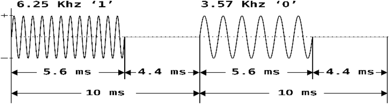
PCM/FSK signal at the buffer output of TE.
The TE FPGA board has an unique feature of having both the TE and TD functionality implemented in the FPGA. It is like having a built-in TD to check in real-time the correctness of the transmitted command and abort the command on detection of any error. The TD outputs appear on the pins of the Flat Ribbon Cable (FRC) connectors and the LEDs of the board shown in Figure 2(b). If a LED light emitting diode assembly is connected to the FRC connectors it will indicate the command executed.
3.2 FPGA based TD design
The block diagram of FPGA centered TD is exhibited in Figure 5. This is the FPGA board exclusively designed by us for this application. It is a 6-layer printed circuit board of size 110 × 110 mm and comprises following components:
XC6SLX9-2FTG256I—Xilinx Spartan 6 FPGA
XCF04VOG20C—Xilinx 4 MB Serial Flash PROM
IN4454—switching diode
HCF4001BM—NOR gate
MC14504BDG—3.3 V–5 V buffered level shifter
50 MHz MEMS oscillator clock of stability +/− 10 ppm
5 V, −5 V, 3.3 V and 1.2 V Regulators
JTAG for programming
LT1014ISW—quad op-amp

Telecommand Decoder. (a) Block diagram of TD; (b) Custom designed FPGA based TD.
The demodulated output from receiver in Figure 5 is the same PCM/FSK signal as shown in Figure 4, with a voltage of 2 V–5 V peak to peak, depending on the signal strength received. This PCM/FSK signal passes through two separate chains of BPF’s and pulse shaping circuits before being fed to the FPGA. BPF ‘0’ allows only 3.57 KHz sinewaves while BPF ‘1’ allows only 6.25 KHz sinewaves. Receiving ZERO’s and ONE’s on separate inputs makes bit detection easy. Although 35 pulses are received for a logical ‘1’ only 18 pulses are checked to detect the bit. Similarly, though 20 pulses are received for logical ‘0’, only 13 are checked for bit detection. BPF’s are designed using LT1014 op-amp. Pulse shaper using diode, NOR gates and voltage level shifter convert the bipolar sinewaves into digital pulses of 3.3 V to make it compatible with the FPGA. The FPGA does all the decoding, explained in Section 2, and generates a corresponding command output which is used to drive relays or transfer data based on the type of command received. Since the relays operate at 5 V, the FPGA outputs are level shifted from 3.3 V to 5 V using MC14504BDG IC and are routed through the two D type 26 pin connectors and the FRC connectors. The data commands are sent through the 15 pin D type connector (8 data bits and three strobe pulses). The design of the circuitry other than the FPGA, that is, buffer, BPF’s and Pulse shaper, has not been changed from the existing design as it is a tested and tried one. The relays were not incorporated as the idea was to first implement and validate the decoder part in a FPGA board. The FPGA based TE and TD was extensively tested and no anomalies were noticed. The current drawn by the FPGA is just 40 mA at +5 V. As TD is an on-board system, low power consumption is a big advantage. In addition, the size and mass too are drastically reduced when compared with the discrete IC based TD.
4 Simulation results
The essence of using a FPGA is that the code written for the hardware can be simulated and all parameters can be checked in the simulation before freezing the design. This saves a lot of time during the design phase. To make the report simple only few simulation results are presented. For simulation, a code called test bench is written wherein the required inputs are introduced in the code and the output is checked from the simulation results.
The system clock for the TE and TD is a 50 MHz oscillator. A one MHz clock is generated from this. The VHDL code is written in behavioral style of modeling. All the processes in the code run with respect to one MHz clock. The simulation results are shown in Figure 6. The TE simulation for command 9006 is shown in Figure 6(a). The simulation is run for a duration of 2 frames. All the signals are as expected and are self-explanatory. In Figure 6(b) flags are the 3.57 KHz and 6.25 KHz selection signal to the MUX of TE. Figure 6(c) is the TD simulation for command 9006. The received and the TD generated frame (comd_frame [0:30] in simulation) are equal and hence the sixth ON/OFF (pulse_cmd_op [1:63] in simulation) command output goes high, while the DATA command strobe remains unchanged. Figure 6(d) is the TD simulation for command 8906. As expected, all the 63 ON/OFF command outputs remain unchanged but the DATA command strobe (data_cmd_stro [1:3] in simulation) goes high. The first bit is the strobe pulse for 89XX, second is for the 8AXX and the third bit is for 8BXX command. The 8 bit data (comd_data [0:7] in simulation) too is extracted correctly for transfer to any one of the sub-systems. The device utilization summary for both TE and TD in one FPGA is as follows: (1) Number of Slice registers used is 1802 out of available 11,440 which is 15 %. (2) Number of Slice LUTs used is 3419 out of 5720 which is 59 %.

Simulation results. (a) TE simulation for command 9006; (b) TE simulation showing 3.57 KHz and 6.25 KHz MUX selection signal (flags); (c) TD simulation for decoding command 9006; (d) TD simulation for decoding DATA command 8906.
The simulation result of the command 8006 is represented in Figure 7. The simulation incorporates a command comparison logic that automatically rejects any command, that has been impaired either by the channel or receiver noise. This logic ensures that only the proper command will be executed and false commands will never be executed. In general, valid commands are begun with the hexadecimal. Otherwise, the remaining commands are considered as errors. Here, the invalid comment 8006 is sent and the 3.57 KHz and 6.25 KHz are the selection signal to the MUX of TE. The simulation is run for the duration of 1 frame. The received and the TD-generated frame (comd_frame [0:30] in simulation) are equal. But, the pcm_out is zero. Hence, the commands are rejected by the decoder.

Illustrates the simulation for command 8006.
4.1 Performance analysis based on objectives
In this subsection, the performance of the proposed framework is analysed and compared with the existing telecommand system based on the whole system’s efficiency. Commands were sent to TIFR TD and proposed FPGA based TD, at a very low signal acceptance level. It was noticed that FPGA based TD command acceptance level was ∼ 96 % while TIFR TD acceptance level was 90 % as shown in Figure 8. FPGA based TD is not only more efficient, but also consumes less power and is 40 % smaller in size and weight compared to the TIFR TD. These benefits makes it an ideal candidate for balloon-borne applications wherein efficiency, size, weight and power is a critical requirement.

A comparative analysis.
5 Conclusions
In this paper, we presented the design, development and implementation of BCH (31,16) telecommand encoder and decoder using FPGA. The code is written in VHDL. Simulation and synthesis are done using Xilinx ISE 14.7 design suite. The simulation and tests show that the performance is satisfactory. Using FPGA has led to drastic reduction in size, weight and power consumption which is essential for balloon experiments. As a future step, the TD will be implemented with relays in high pin count and more advanced FPGA to increase the number of Commands and also add more features. In addition, the analog circuits will be replaced with analog to digital converters so that all processing is done digitally.
Funding source: The authors thank the engineers from the Control Instrumentation for Balloon group at BF Hyderabad, for the help during the testing phase, and the Department of Atomic Energy, Government of India, for support under Project Identification
Award Identifier / Grant number: RTI 4002
-
Author contributions: All Authors contributed to the design and methodology of this study, the assessment of the outcomes and the writing of the manuscript.
-
Research funding: The authors thank the engineers from the Control Instrumentation for Balloon group at BF Hyderabad, for the help during the testing phase, and the Department of Atomic Energy, Government of India, for support under Project Identification code No. RTI 4002.
-
Conflict of interest statement: There is no conflict of interest among the authors.
References
Anand, D., B. S. Kumar, and D. K. Ojha. 2021. “TIFR Zero-Pressure Balloon Programme Crosses a Milestone.” Current Science 120 (1): 1672–8. https://doi.org/10.18520/cs/v120/i11/1672-1678.Search in Google Scholar
Bansiya, R. D. 1987. “Microprocessor Based On-Board Telecommand System for Spacecraft.” Journal of the Indian Institute of Science 67: 453–64.Search in Google Scholar
Gosh, S. K., and S. N. Tandon. 1982. “A Telecommand System for Balloon Payloads.” Journal of Physics E: Scientific Instruments 15 (7): 755–9. https://doi.org/10.1088/0022-3735/15/7/016.Search in Google Scholar
Kasturirangan, K., S. Pal, B. L. Agarwal, and R. K. Rajangam. 1993. “Spacecraft Electronics.” IETE Technical Review 10 (5): 429–50. https://doi.org/10.1080/02564602.1993.11437370.Search in Google Scholar
Lin, S., and D. J. CostelloJr. 1983. Error Control Coding, Fundamentals and Applications. New Jersey: Prentice-Hall.Search in Google Scholar
Prasad, S. N., and S. Pal. 2003. “Telemetry, Tracking and Command Systems of Spacecraft.” IETE Technical Review, 20 (6): 561–76. https://doi.org/10.1080/02564602.2003.11417116.Search in Google Scholar
Wallace, H. 2001. Error Detection and Correction Using the BCH Codes. Copyright 2001.Search in Google Scholar
© 2024 the author(s), published by De Gruyter, Berlin/Boston
This work is licensed under the Creative Commons Attribution 4.0 International License.
Articles in the same Issue
- Solar photovoltaic-integrated energy storage system with a power electronic interface for operating a brushless DC drive-coupled agricultural load
- Analysis of 1-year energy data of a 5 kW and a 122 kW rooftop photovoltaic installation in Dhaka
- Reviews
- Real yields and PVSYST simulations: comparative analysis based on four photovoltaic installations at Ibn Tofail University
- A comprehensive approach of evolving electric vehicles (EVs) to attribute “green self-generation” – a review
- Exploring the piezoelectric porous polymers for energy harvesting: a review
- A strategic review: the role of commercially available tools for planning, modelling, optimization, and performance measurement of photovoltaic systems
- Comparative assessment of high gain boost converters for renewable energy sources and electrical vehicle applications
- A review of green hydrogen production based on solar energy; techniques and methods
- A review of green hydrogen production by renewable resources
- A review of hydrogen production from bio-energy, technologies and assessments
- A systematic review of recent developments in IoT-based demand side management for PV power generation
- Research Articles
- Hybrid optimization strategy for water cooling system: enhancement of photovoltaic panels performance
- Solar energy harvesting-based built-in backpack charger
- A power source for E-devices based on green energy
- Theoretical and experimental investigation of electricity generation through footstep tiles
- Experimental investigations on heat transfer enhancement in a double pipe heat exchanger using hybrid nanofluids
- Comparative energy and exergy analysis of a CPV/T system based on linear Fresnel reflectors
- Investigating the effect of green composite back sheet materials on solar panel output voltage harvesting for better sustainable energy performance
- Electrical and thermal modeling of battery cell grouping for analyzing battery pack efficiency and temperature
- Intelligent techno-economical optimization with demand side management in microgrid using improved sandpiper optimization algorithm
- Investigation of KAPTON–PDMS triboelectric nanogenerator considering the edge-effect capacitor
- Design of a novel hybrid soft computing model for passive components selection in multiple load Zeta converter topologies of solar PV energy system
- A novel mechatronic absorber of vibration energy in the chimney
- An IoT-based intelligent smart energy monitoring system for solar PV power generation
- Large-scale green hydrogen production using alkaline water electrolysis based on seasonal solar radiation
- Evaluation of performances in DI Diesel engine with different split injection timings
- Optimized power flow management based on Harris Hawks optimization for an islanded DC microgrid
- Experimental investigation of heat transfer characteristics for a shell and tube heat exchanger
- Fuzzy induced controller for optimal power quality improvement with PVA connected UPQC
- Impact of using a predictive neural network of multi-term zenith angle function on energy management of solar-harvesting sensor nodes
- An analytical study of wireless power transmission system with metamaterials
- Hydrogen energy horizon: balancing opportunities and challenges
- Development of renewable energy-based power system for the irrigation support: case studies
- Maximum power point tracking techniques using improved incremental conductance and particle swarm optimizer for solar power generation systems
- Experimental and numerical study on energy harvesting performance thermoelectric generator applied to a screw compressor
- Study on the effectiveness of a solar cell with a holographic concentrator
- Non-transient optimum design of nonlinear electromagnetic vibration-based energy harvester using homotopy perturbation method
- Industrial gas turbine performance prediction and improvement – a case study
- An electric-field high energy harvester from medium or high voltage power line with parallel line
- FPGA based telecommand system for balloon-borne scientific payloads
- Improved design of advanced controller for a step up converter used in photovoltaic system
- Techno-economic assessment of battery storage with photovoltaics for maximum self-consumption
- Analysis of 1-year energy data of a 5 kW and a 122 kW rooftop photovoltaic installation in Dhaka
- Shading impact on the electricity generated by a photovoltaic installation using “Solar Shadow-Mask”
- Investigations on the performance of bottle blade overshot water wheel in very low head resources for pico hydropower
- Solar photovoltaic-integrated energy storage system with a power electronic interface for operating a brushless DC drive-coupled agricultural load
- Numerical investigation of smart material-based structures for vibration energy-harvesting applications
- A system-level study of indoor light energy harvesting integrating commercially available power management circuitry
- Enhancing the wireless power transfer system performance and output voltage of electric scooters
- Harvesting energy from a soldier's gait using the piezoelectric effect
- Study of technical means for heat generation, its application, flow control, and conversion of other types of energy into thermal energy
- Theoretical analysis of piezoceramic ultrasonic energy harvester applicable in biomedical implanted devices
- Corrigendum
- Corrigendum to: A numerical investigation of optimum angles for solar energy receivers in the eastern part of Algeria
- Special Issue: Recent Trends in Renewable Energy Conversion and Storage Materials for Hybrid Transportation Systems
- Typical fault prediction method for wind turbines based on an improved stacked autoencoder network
- Power data integrity verification method based on chameleon authentication tree algorithm and missing tendency value
- Fault diagnosis of automobile drive based on a novel deep neural network
- Research on the development and intelligent application of power environmental protection platform based on big data
- Diffusion induced thermal effect and stress in layered Li(Ni0.6Mn0.2Co0.2)O2 cathode materials for button lithium-ion battery electrode plates
- Improving power plant technology to increase energy efficiency of autonomous consumers using geothermal sources
- Energy-saving analysis of desalination equipment based on a machine-learning sequence modeling