Comparative assessment of high gain boost converters for renewable energy sources and electrical vehicle applications
-
J. Veerabhadra
 and
Sulake Nagaraja Rao
and
Sulake Nagaraja Rao

Abstract
Due to greenhouse gas emissions and the energy crisis, the conventional way of generation of electricity using fossil fuels is being substituted with Renewable Energy Sources (RES) like solar photovoltaics (SPV), fuel cells, wind, etc. The voltage produced by RES is very small in magnitude; therefore, the choice of DC–DC converter is critical for regulating and improving the output of RES to its maximum level. To meet the power requirement for the utility grid and electric vehicles (EV), the voltage must be enhanced. So far, various types of high-gain DC–DC boost converter (HG-BC) topologies have been suggested. An overview of HG-BC topologies for RES and EV applications is presented in this paper, which provides a unique, extensive, perceptive, and comparative analysis of HG-BC topologies. The mathematical modeling and operating principles of each converter topology have been analyzed and discussed. The boost factor (B) and component count for various HG-BC are thoroughly compared for a 0.5 duty cycle using the MATLAB/Simulink tool.
1 Introduction
The exponential rise in global population results in the rise in energy demand. Because of greenhouse gas emissions, meeting the global energy needs using traditional methods of power generation harms the environment and causes energy shortages (Acar and Dincer 2017; Hossain et al. 2018; Khare et al. 2013; Perera 2018; Reddy 2021; Zhang et al. 2016). As a result, RES like SPV, fuel cells, and wind are replacing the generation of electricity from fossil fuels (Pranupa, Sriram, and Nagaraja Rao 2022). These RES have been expanding quickly and are expected to triple in the near future (Forouzesh et al. 2017; Manikandan and Vadivel 2013; Mumtaz et al. 2021; Purushothaman et al. 2022; Raghavendra et al. 2019; Shahir et al. 2017). RES presently accounts for 25% of electricity generation capacity across the global. RES is not only efficient, but also beneficial to the environment and low-maintenance. To meet the power requirements for the utility grid and EV, the RES system must integrate a suitable HG-BC to boost and vary the output voltage (V out) (Ali et al. 2014; Forouzesh et al. 2017; Kabalo et al. 2010; Navamani et al. 2022; Raghavendra et al. 2019; Radhika and Margaret 2021; Zaid et al. 2021). The various types of HG–BC are investigated in detail (Ahmad et al. 2018; Aihsan et al. 2022; Dawood 2016; Gore et al. 2019; Hasanpour et al. 2022; Mansour et al. 2022; Raveendhra et al. 2022; Radhika and Margaret 2021; Suryoatmojo et al. 2018; Wu et al. 2015). The RES output voltage is low in magnitude; therefore, the choice of DC–DC converter is critical for varying and improving to get the highest V out.
The transition from traditional, depletable energy sources to renewable, sustainable energy sources necessitates adaptive, high-efficiency power electronic converters and energy infrastructure (Alghaythi et al. 2020; Elsayad et al. 2018; Hossain et al. 2018; Meinagh et al. 2019; Mumtaz et al. 2021; Naresh et al. 2021; Rahimi et al. 2021; Wu et al. 2015; Zaid et al. 2021, 2022). The need for high DC voltage necessitates the use of HG-BC. The HG-BC is employed in a wide range of industries, including solar PV, robotics, aerospace, medical equipment, high voltage DC systems, and EVs (Jagadeesh and Indragandhi 2022; Mansour and Zaky 2023; Matam et al. 2018; Navamani et al. 2022; Rehman et al. 2015; Samuel et al. 2020; Sivakumar et al. 2016).
A typical RES incorporated with HG-BC is depicted in Figure 1. The voltage of the SPV and fuel cell is DC, and they are coupled directly to a low-voltage DC bus. The output of a wind turbine is AC, which must be converted into DC and then given to a low-voltage DC bus. The RES system V out is low, and it is required to be converted into high-voltage DC for utility grid and EV applications. Therefore, the use of HG-BC is essential.
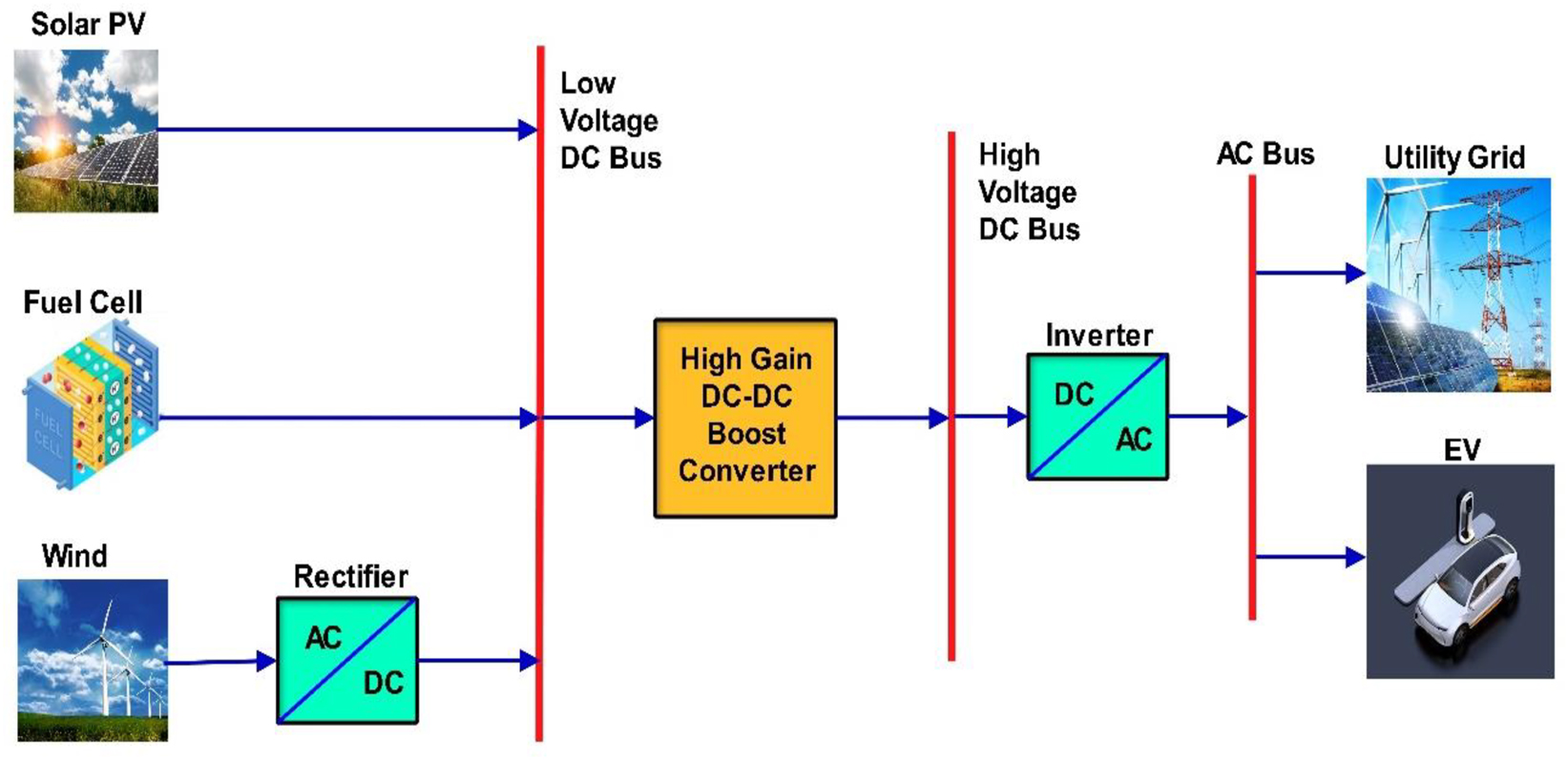
A typical RES integrated with HG-BC.
The types of HG-BC for RES and EV applications are depicted in Figure 2. The major focus of this research is on non-isolated HG-BC. The use of passive elements and semiconductor devices, together with regulating the duty cycle of the control circuit, results in a high gain (Dawood 2016; Nagaraja Rao et al. 2022; Radhika and Margaret 2021; Rahimi et al. 2021; Raveendhra et al. 2022; Wu et al. 2015).
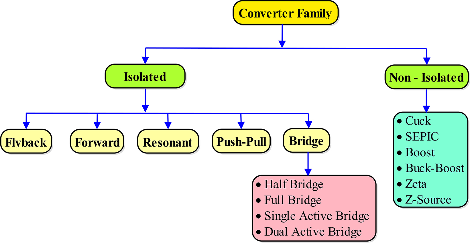
Classifications of DC–DC converter for RES and EV applications.
In comparison to the input voltage, the voltage in BC is higher (Varanasi, Nagaraja Rao, and Duraiswamy 2023). For a buck-boost converter, the polarity of the converter voltage is inverted, and the magnitude of the V out is increased or decreased. The Cuk converter’s output is also inverted, producing voltages of greater or lesser magnitude. The Cuk and Buck-Boost converters’ gain remains constant (Chandrasekar et al. 2020). The SEPIC converter can be used to raise or lower the V out without reversing the output polarity (Moradpour et al. 2017; Maroti et al. 2019; Sabzali et al. 2015). The Z-Source converter is an efficient converter. The features of this converter is to step up and down the V out (Rao, Veerabhadra, and Kumar 2020; Torkan and Ehsani 2018). The topology of the Zeta converter is also called the power optimizer. The features of this converter are constant output current, non-inverting operation, and controlled output voltage. The ripple content in the V out is low (Hosseini et al. 2015; Keerthana and Chintu 2017).
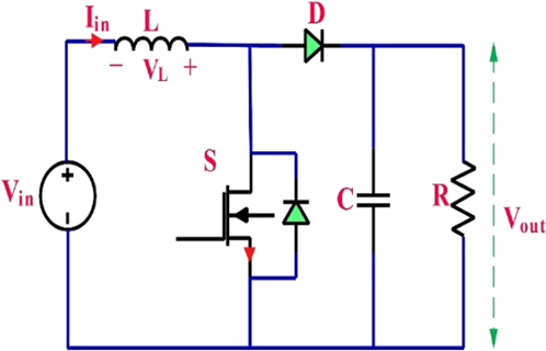
The conventional BC is shown in Figure 3. The output is too low for utility grid supply, and the boost factor is adjusted to 2. One of the main drawbacks of traditional BC is its low value of B.
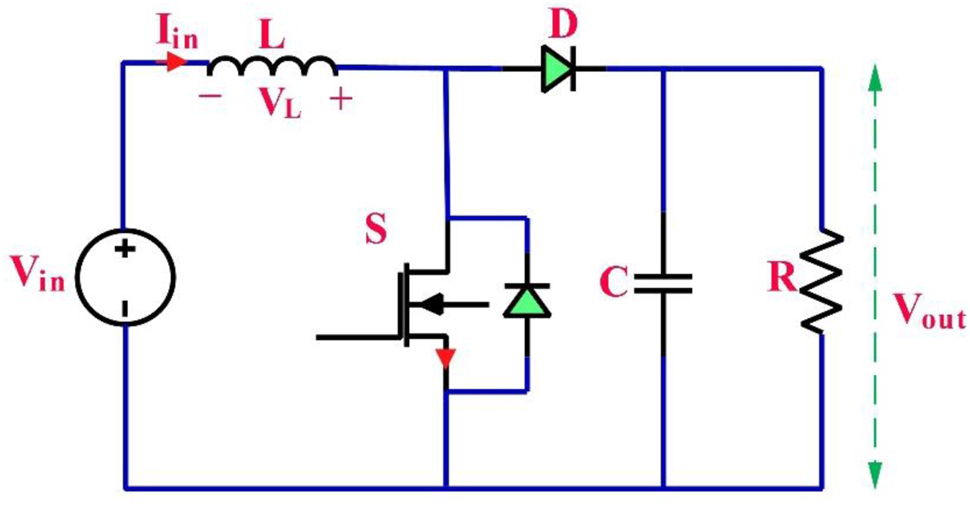
Conventional boost converter.
The gain of conventional BC is given by
For a 0.5 duty cycle, the value of B equals 2. With the use of HG-BC, the limitations of conventional BC can be overcome.
In this paper, the following HG-BC are discussed in detail in terms of operation, mathematical modeling, and comparison, with component count and boost factor (B):
Conventional Boost Converter (BC)
High Gain Quadratic Following Boost Converter(HG-QFBC)
High Gain Quadratic Boost converter (HG-QBC)
High Gain Interleaved Boost Converter (HG-IBC)
High Gain Improved Quadratic Boost Converter (HG-IQBC)
High Gain Cubic Boost Converter (HG-CBC)
Furthermore, simulation of the aforementioned HG-BC topologies has been performed using the MATLAB/Simulink tool. The primary goal of this research is to afford a detailed, perceptive, and comparative analysis of HG-BC topologies.
2 Mode of operation and mathematical analysis of HG-QFBC topology
2.1 Operation of HG-QFBC topology
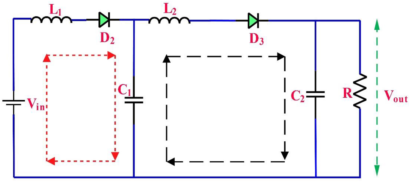
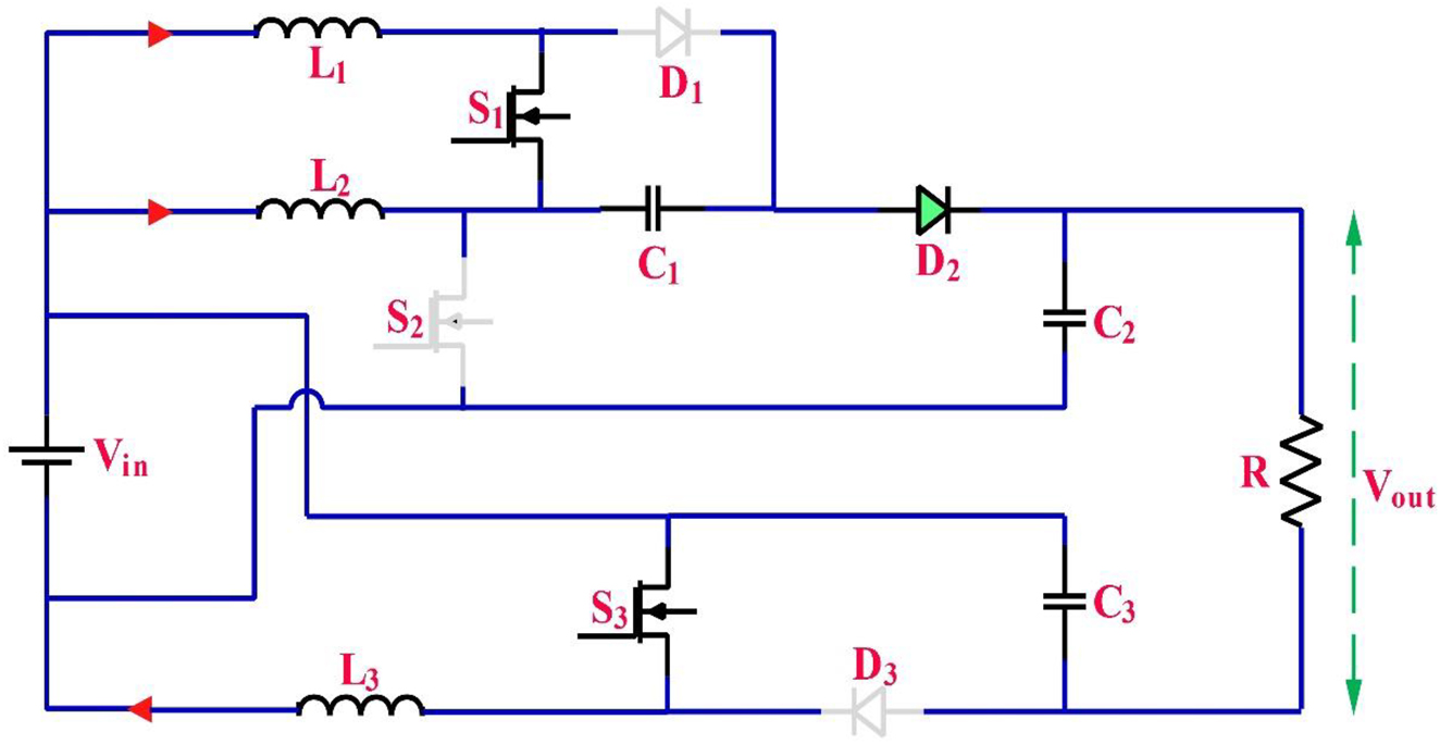
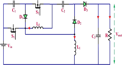
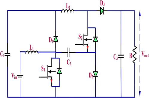
The suggested HG-QFBC is depicted in Figure 4. It comprises of two semiconductor switches (S 1 and S 2), three diodes (D 1, D 2 and D 3), three capacitors (C 1, C 2 and C 3), two inductors (L 1 and L 2), and at last resistive load (R). The HG-QFBC uses a two switches (S 1 and S 2) to regulate the V out.
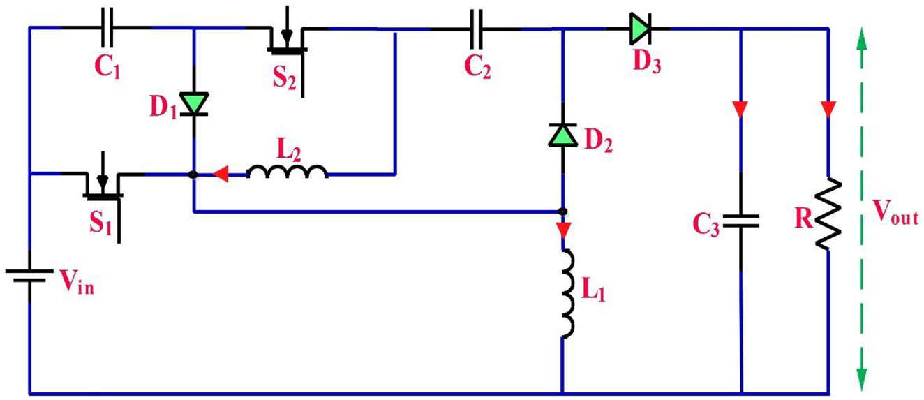
HG-QFBC connected to RES.
2.2 Mode of operation – I
The operating mode-1 of HG-QFBC is represented in Figure 5. It comprises of two semiconducting switches (S 1 and S 2) that will be turned on constantly. An open circuit will be formed by the two diodes (D 1 and D 3). The diode (D 2) will be in conduction. The input source charges the L 1, the inductor (L 2) is excited by the capacitors’ (C 1 and C 2) voltage, and the capacitor (C 3) delivers current to the resistive load (R).
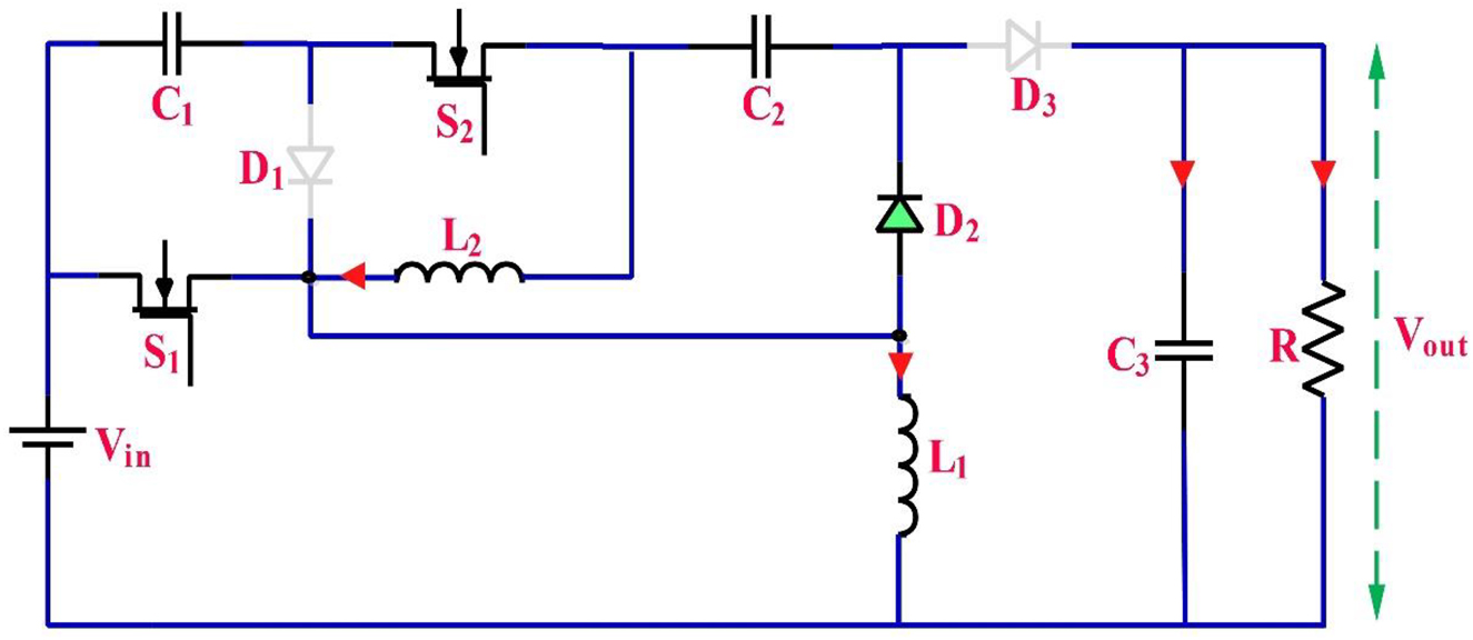
Mode of operation-I of HG-QFBC.
The voltage of (L 1 and L 2) is derived by applying KVL to Figure 5.
2.3 Mode of operation – II
The mode of operation II for HG-QFBC is represented in Figure 6. The two semiconducting switches (S 1 and S 2) will be switched off. The first two diodes (D 1 and D 3) will be in conduction mode, while the third (D 2) will become open. L 1 and L 2 will demagnetize and charge C 1, C 2, and C 3.
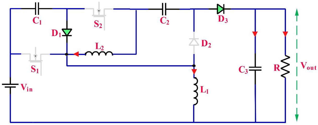
Mode – II operation of HG-QFBC.
The voltage of (L 1 and L 2) is obtained by using KVL to Figure 6.
2.4 Mathematical analysis
The voltage of each inductors (L 1 and L 2) is determined using volt-sec balance.
The voltage of L 1 is obtained as
The voltage of C 1 is obtained as
The voltage across L 2 is given by
The voltage of C 2 is obtained as
The gain (G) of the HG-IQBC is given as
The equation (17) represents, G of the HG-QFBC. For 0.5 duty cycle (D), the value of B is 3.
3 Mode of operation and mathematical analysis of HG-QBC topology
3.1 Operation of HG-QBC topology
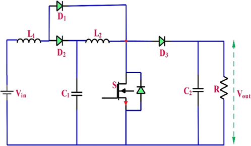
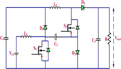
The topology of HG-QBC is shown in Figure 7. It comprises a switch (S), three diodes (D 1, D 2, and D 3), two capacitors (C 1 and C 2), two inductors (L 1 and L 2), and at last a resistive load (R). The HG-QBC uses only one switch (S) to regulate the V out.
HG-QBC connected to RES.
3.2 Mode of operation-I
The operating mode I of HG-QBC is represented in Figure 8. The switch (S) is switched on, and the diode (D 1) will conduct. The diodes (D 2 and D 3) will form an open circuit. The voltage from the input source will charge the inductor (L 1) and capacitor (C 1). The charged capacitor (C 2) helps deliver current to the resistive load (R).
Mode-I operation of HG-QBC.
The voltages of (L 1, and L 2) is derived by applying KVL to Figure 8.
3.3 Mode of operation – II
The mode of operation II for HG-QBC is represented in Figure 9. The switch (S) is switched off. The diode (D 1) will be open, and the other two diodes (D 2 and D 3) are in conduction mode. The inductors (L 1 and L 2) will be de-energized, and the capacitors (C 1 and C 2) will get charged.
Mode of operation-II for HG-QBC.
The voltage of (L 1 and L 2) is derived by applying KVL to Figure 9.
3.4 Mathematical analysis
By using the volt-sec balance, the voltages of (L 1, and L 2) is determined.
The voltage across L 1
The capacitor (C 1) voltage is obtained as
The voltage across L 2 is obtained as
The capacitor (C 2) voltage is given as
The G of HG-QBC is obtained as
The G of HG-QBC is represented by equation (33). The boost factor is 4 for a 0.5 D.
4 Mode of operation and mathematical analysis of HG-IBC topology
4.1 Operation of HG-IBC topology
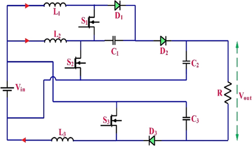
The suggested HG-IBC is represented in Figure 10. It contains three semiconducting switches (S 1, S 2, and S 3), three diodes (D 1, D 2, and D 3), three capacitors (C 1, C 2, and C 3), three inductors (L 1, L 2, and L 3), and at last a resistive load (R). The suggested HG-IBC uses three switches (S 1, S 2, and S3) to control the V out.
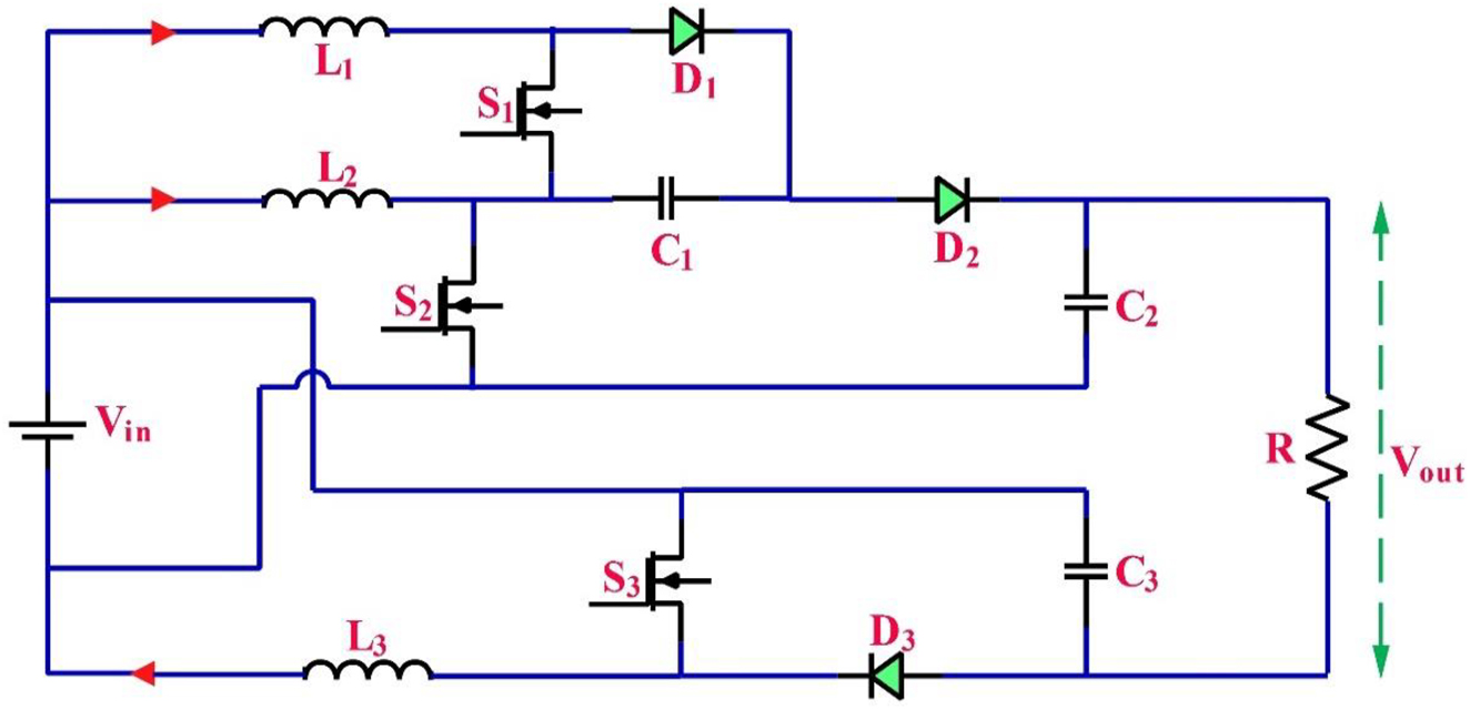
HG-IBC connected to RES.
4.2 Mode of operation-I
The operating mode I of HG-IBC is represented in Figure 11. It contains three semiconducting switches (S 1, S 2, and S 3) that will be switched on simultaneously. The three diodes (D 1, D 2, and D 3) will become an open circuit. The input source energizes the L 1, L 2, and L 3. C 1 is disconnected from the input supply and the loading. The voltages of the capacitors (C 2 and C 3) delivers the current to the resistive load (R).
Mode of operation-I for HG-IBC.
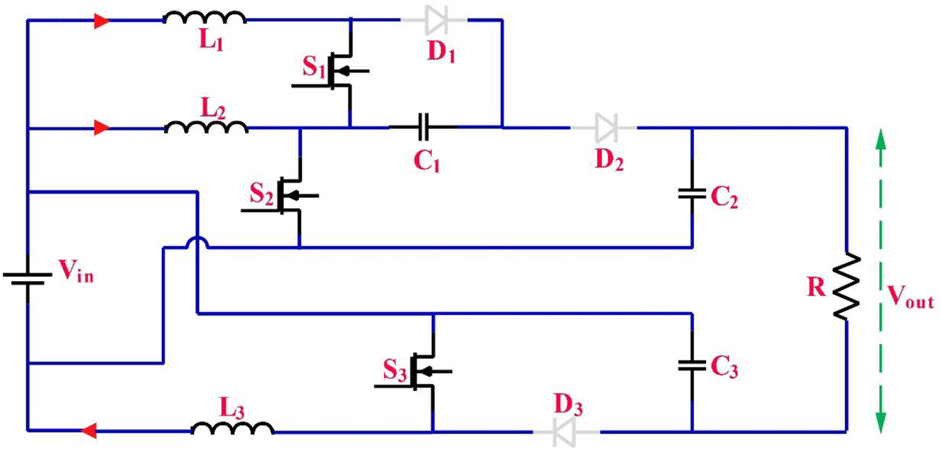
4.3 Mode of operation-II
The mode of operation II for HG-IBC is represented in Figure 12. The switches (S 1 and S 3) will be deactivated by being turned off, and the switch (S 2) will be on. The two diodes (D 1 and D 3) will be in conduction, and the third diode (D 2) will be turned off due to an open circuit. The two capacitors (C 1 and C 3) will get charged from the input source. The voltage supplied by the capacitor (C 2) delivers the current to the resistive load (R).
Mode of operation-II for of HG-IBC.
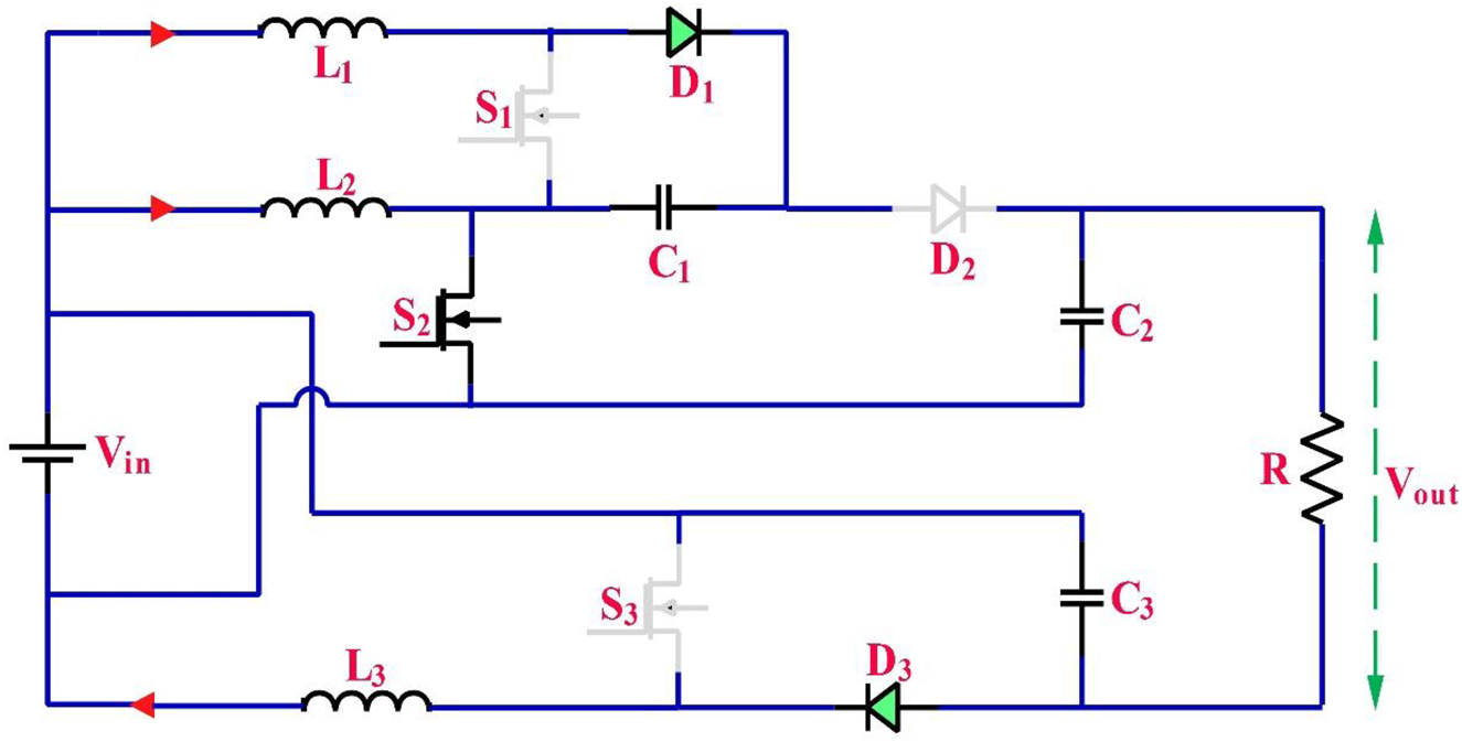
4.4 Mode of operation-III
The operating mode III of the HG-IBC is represented in Figure 13. This operating mode is just the reverse of mode II operation. The switches (S 1 and S 3) will be on and the other switch (S 2) will be switched off. The two diodes (D 1 and D 3) will be turned off due to the open circuit, and the third diode (D 2) will be in conduction. The capacitor (C 2) will get charged from the input source. The two capacitors (C 1 and C 3) deliver the current to the resistive load (R).
Mode of operation-III for HG-IBC.
4.5 Mathematical analysis
The voltages of L 1, L 2 and L 3 is determined using volt-sec balance.
The voltage of L 1 is given as
The capacitor (C 1) voltage is obtained as
The voltage of L 2 is obtained as
The capacitor (C 2) voltage is given as
By substituting the above equation (35) in (37), we get
The voltage of L 3 is obtained as
The capacitor (C 3) voltage is given as
The voltage output of HG-IBC is given as
The G of the HG-IBC is given as
The G of HG-IBC is represented in equation (43). The value of boost factor is 5 for 0.5 D.
5 Mode of operation and mathematical analysis of HG-IQBC topology
5.1 Operation of HG-IQBC topology
The suggested HG-IQBC is depicted in Figure 14. It contains two semiconductor switches (S 1 and S 2), three diodes (D 1, D 2, and D 3), three capacitors (C 1, C 2, and C 3), two inductors (L 1 and L 2), and, at last, the resistive load (R). The HG-IQBC converter uses two switches (S 1 and S 2) to regulate the V out.
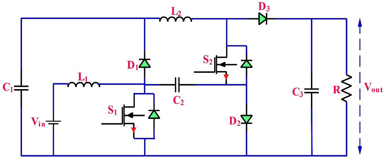
HG-IQBC connected to RES.
5.2 Mode-I operation
The HG-IQBC for mode I of operation is represented in Figure 15. It consists of two semiconducting switches (S 1 and S 2) that will be switched on constantly. The three diodes (D 1, D 2, and D 3) will be switched off and become an open circuit. The inductor (L 1) will get charged from the input source, the voltage supplied by two capacitors (C 1 and C 2) will energize the L 2, and the voltage across C 3 will deliver the current to the resistive load (R).
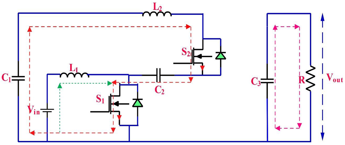
Mode-I operation of HG-IQBC.
The voltage of (L 1 and L 2) is derived by applying KVL to Figure 15.
5.3 Mode of operation-II
The suggested mode of operation II for HG-IQBC is represented in Figure 16. The two semiconducting switches (S 1 and S 2) will be off. The three diodes (D 1, D 2, and D 3) will be in conduction. The inductors (L 1 and L 2) will be de-energized, and the capacitors (C 1, C 2, and C 3) will get charged.
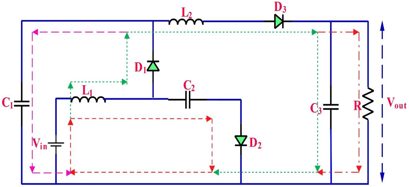
Mode of operation-II for HG-IQBC.
The inductors (L 1 and L 2) voltage is derived by applying KVL to Figure 16.
5.4 Mathematical analysis
The voltage of Inductors (L 1 and L 2) is used to determine by applying volt-sec balance.
The voltage across L 1 is obtained as
The capacitor (C 1 and C 2) voltage is given as
The voltage of L 2 is given by
The capacitor (C 3) voltage is given as
The gain of the HG-IQBC is obtained as
The equation (58) represents the gain of HG-IQBC. The boost factor is 6 for 0.5 duty cycle (D).
6 Mode of operation and mathematical analysis of HG-CBC topology
6.1 Operation of HG-CBC topology
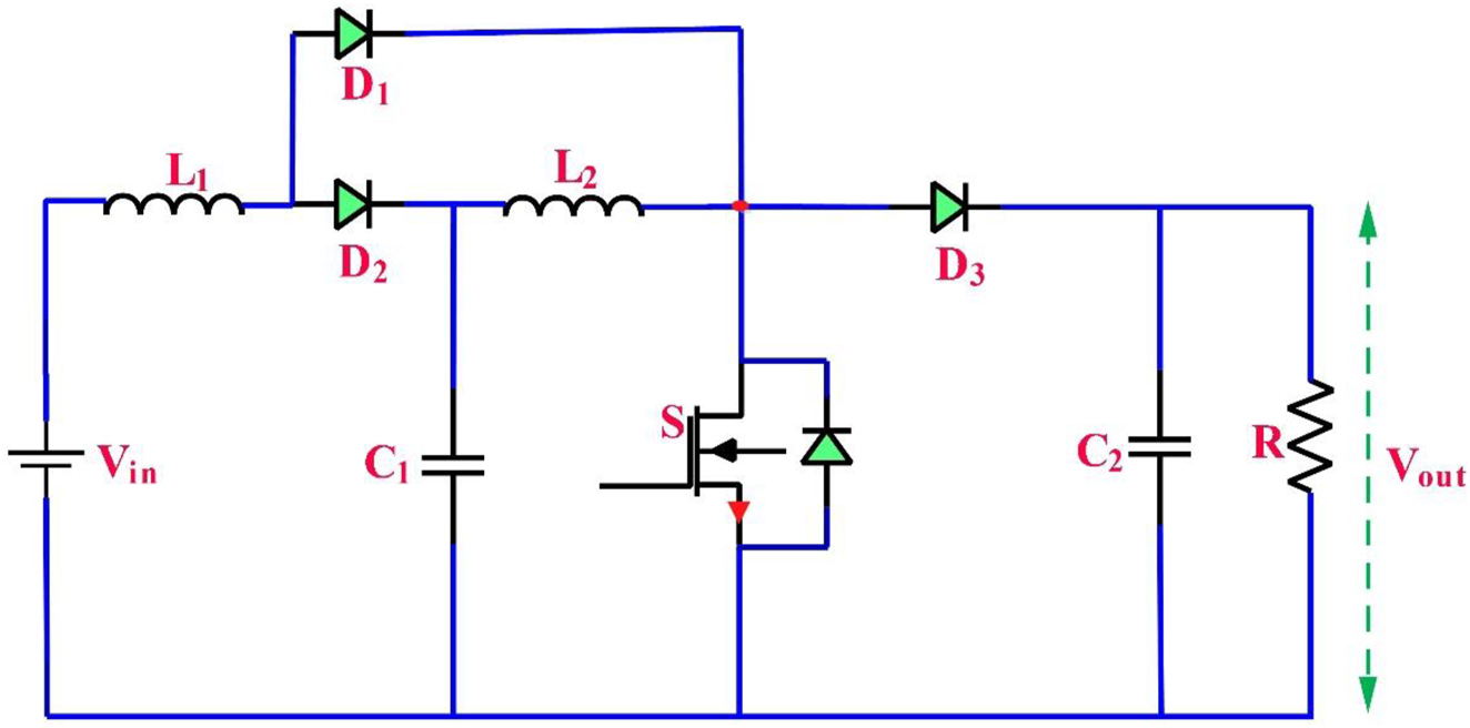
The suggested HG-CBC is shown in Figure 17. It contains one semiconducting switch (S), three inductors (L 1, L 2, and L 3), three capacitors (C 1, C 2, and C 3), five diodes (D 1, D 2, D 3, D4, and D5), and a resistive load (R). The HG-CBC uses only one switch (S) to regulate the V out, and it has two modes of operation.
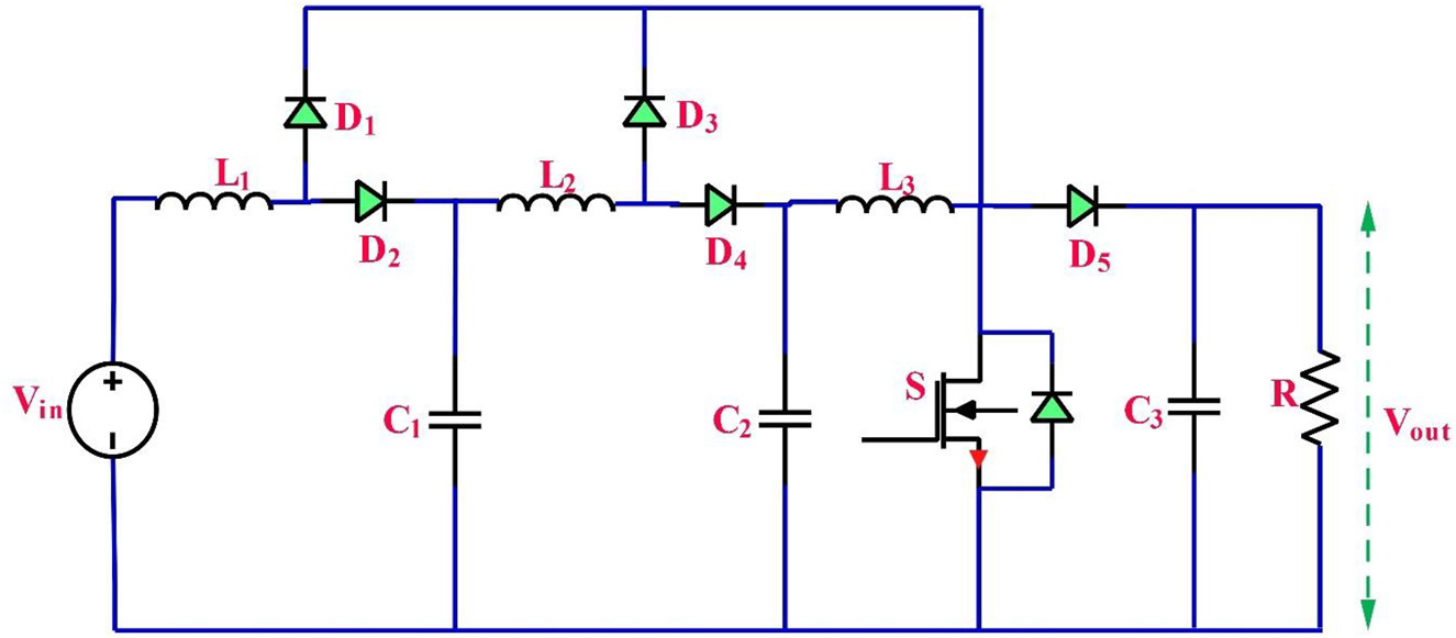
HG-CBC connected to RES.
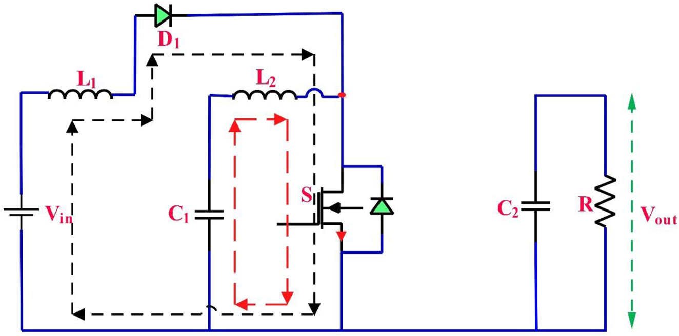
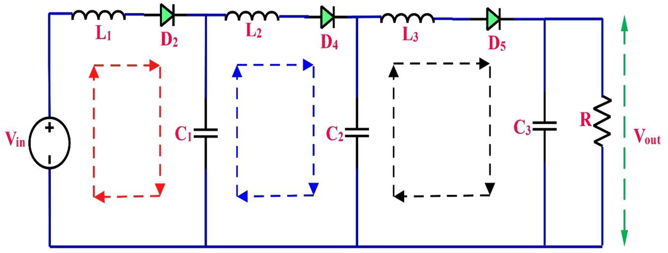
6.2 Mode of operation-I
The operating mode I of HG-CBC is represented in Figure 18. The semiconducting switch (S) is switched on. The two diodes (D 1 and D 3) will be in conduction mode, and the other three diodes (D 2, D 4, and D 5) will act in open circuit. The input source will charge the inductor (L 1), the inductor (L 2) will get excited from the capacitor (C 1) voltage, and finally the inductor (L 3) will be excited from the capacitor (C 2) voltage. The voltage of capacitor (C 3) delivers the current to the resistive load (R).
Mode-I operation of HG-CBC.
The inductors (L 1, L 2 and L 3) voltage is derived by applying KVL to Figure 18.
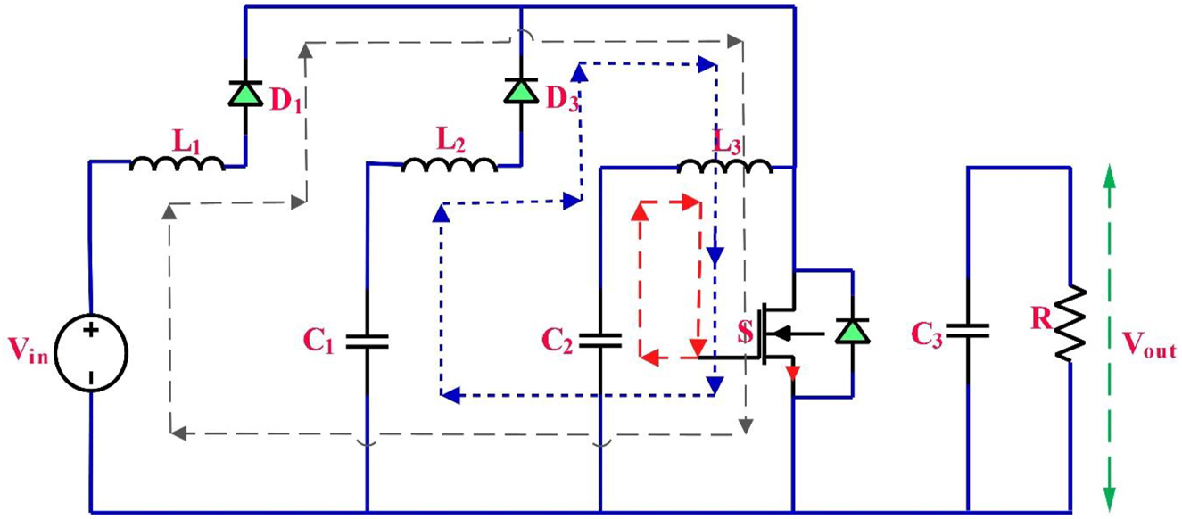
6.3 Mode of operation-II
The circuit diagram in Figure 19 shows the mode of operation II of the HG-CBC. The switch (S) will be switched off. The two diodes (D 1 and D 3) will function as an open circuit, and the other three diodes (D 2, D 4, and D 5) will be under conduction. The inductors (L 1, L 2, and L 3) will be de-energized, and the capacitors (C 1, C 2, and C 3) will get charged.
Mode of operation-II for HG-CBC.
The voltages of (L 1, L 2 and L 3) is derived by applying KVL to Figure 19.
6.4 Mathematical analysis
By employing volt-sec balance, the voltage of L 1, L 2 and L 3 is obtained.
The voltage L 1 is obtained as
The capacitor (C 1) voltage is given as
The voltage of inductor (L 2) is obtained as
The capacitor (C 2) voltage is given as
The voltage of inductor (L 3) is obtained as
The voltage of capacitor C 3 is given by
The gain of HG-CBC is represented in equation (80). The boost factor is 8 for 0.5 duty cycle.
7 Comparative analysis of boost factor for various HG-BC
Figure 20 shows the boost factors for different HG-BC with different duty cycles. For a 0.5 duty cycle, the boost factor (B) for a conventional boost converter is 2. For HG-QFBC, B is equal to 3. The value of B is equal to 4 for HG-QBC. The value of B for HG-IBC is 5. The value of B for HG-IQBC is 6. B for HG-CBC is equal to 8. In comparison with all HG-BC, the highest boost factor for HG-CBC is 8 for 0.5 duty cycle.
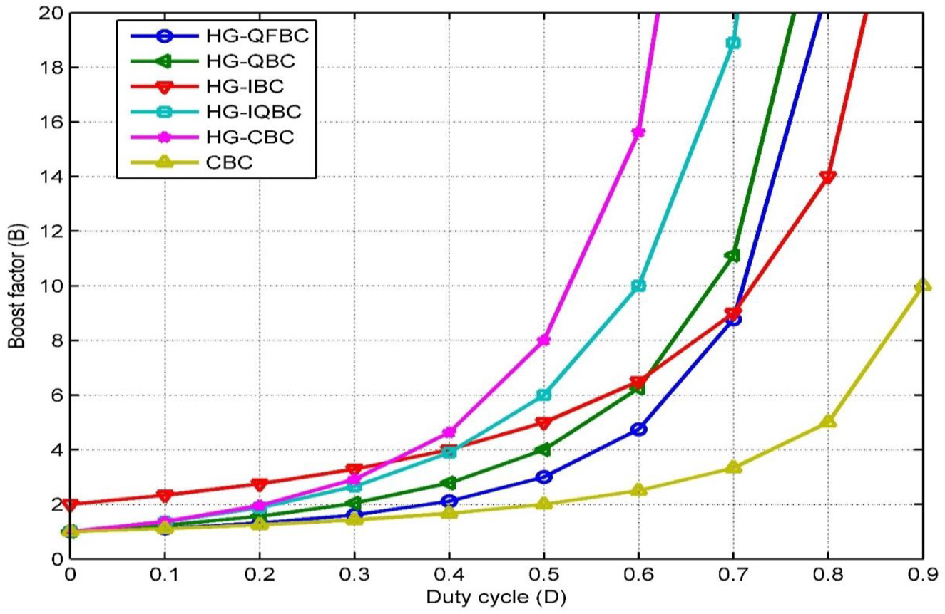
Boost factors of various HG-BC.
Based on component counts and boost factors for 0.5 duty cycle, Table 1 compares various HG-BCs in detail.
Component count and boost factor comparison of various HG-BC.
| Converter type | Voltage gain | Components | B | ||||
|---|---|---|---|---|---|---|---|
| S | D | L | C | Total | |||
| Conventional BC |
|
1 | 1 | 1 | 1 | 4 | 2 |
| HG-QFBC (Veerachary and Kumar 2020) |
|
2 | 3 | 2 | 3 | 10 | 3 |
| HG-QBC (Veerabhadra and Nagaraja Rao 2022) |
|
1 | 3 | 2 | 2 | 8 | 4 |
| HG-IBC (Kumar et al. 2022) |
|
3 | 3 | 3 | 3 | 12 | 5 |
| HG-IQBC (Naresh et al. 2021) |
|
2 | 3 | 2 | 3 | 10 | 6 |
| HG-CBC (Ahmad et al. 2020) |
|
1 | 5 | 3 | 3 | 12 | 8 |
-
Switches (S), Diodes (D), Inductance (L), Capacitance (C) and Boost factor (B).
Table 2 shows a comparative analysis of various boost converter configurations with specifications and features.
A comparative analysis of various HG-BC configurations with the features.
| Sl. No. | Type of converter | Configuration | Specifications | Features |
|---|---|---|---|---|
| 1. | Conventional BC |
|
L = 160 mH C = 220 μF R = 100 Ω Fs = 50 kHz |
The voltage gain of conventional BC is two |
| 2. | HG-QFBC (Veerachary and Kumar 2020) |
|
L
1 = 1600 μH L 2 = 800 μH C 1 = C 2 = 47 μF C 3 = 100 μF R = 300 Ω Fs = 100 kHz |
Enhances the voltage gain and efficiency |
| 3. | HG-QBC (Veerabhadra and Nagaraja Rao 2022) |
|
L
1 = 0.2 mH L 2 = 0.5 mH C 1 = 9 mF C 2 = 2 mF R = 100 Ω Fs = 100 kHz |
Voltage stress is significantly reduced on the switch, diodes, and capacitors. |
| 4. | HG-IBC (Kumar et al. 2022) |
|
L
1 = 0.2 mH L 2 = 0.3 mH L 3 = 5 mH C 1 = 9 μF C 2 = 2 μF C 3 = 1 μF R = 100 Ω Fs = 50 kHz |
Obtains smooth output waveforms with less current and voltage ripples and current ripples |
| 5. | HG-IQBC (Naresh et al. 2021) |
|
L
1 = 0.5 mH L 2 = 1 mH C 1= C 2= 24 μF C 3 = 20 μF R = 100 Ω Fs = 50 kHz |
The voltage gain of an HG-IQBC is six. High boosting with suppression of inrush current |
| 6. | HG-CBC (Ahmad et al. 2020; Revathi and Prabhakar 2016) |
|
L
1 = 0.2 mH L 2 = 0.3 mH L 3 = 1 mH C 1 = 9 mF C 2 = 2 mF C 3 = 1 mF R = 100 Ω Fs = 100 kHz |
High voltage gain with reduced switch stress |
8 Results and discussion
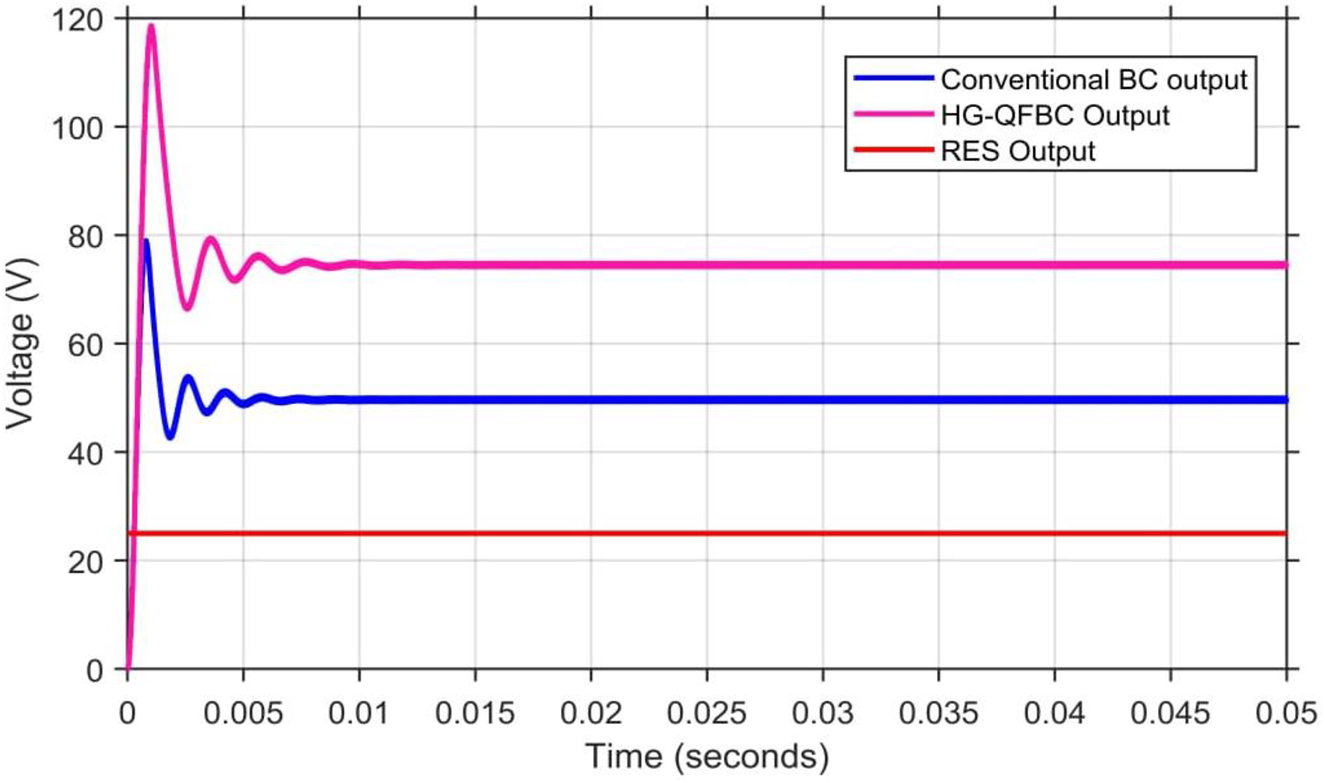
Figure 21 shows the RES voltage output and HG-QFBC. RES’s V out is 25 V, which is very low. It must be improved for grid-connected operation. The conventional BC output is twice the value of the boost factor, resulting in a V out of 50 V. This voltage is insufficient for grid integration. As a result, the X HG-QFBC topology is proposed to improve the output by x three times the boost factor, resulting in a total V out of 75 V.
Output voltage of RES and HG-QFBC.
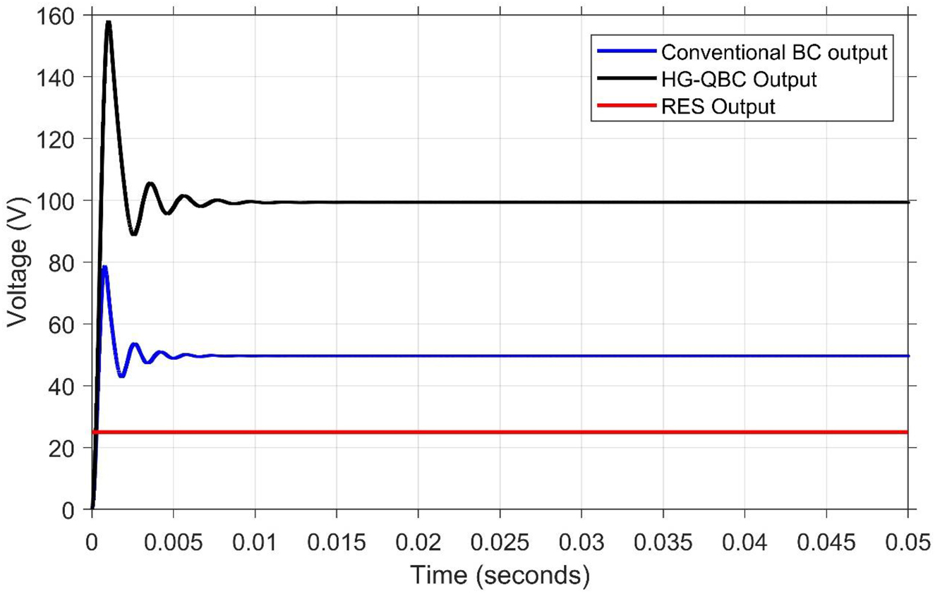
The voltage output of RES and HG-QBC is represented in Figure 22. RES’s V out is 25 V, which is very low. It must be improved for grid-connected operation. The V out of conventional BC is twice the value of the boost factor, resulting in a total V out of 50 V. This voltage is insufficient for grid integration. So, the HG-QBC topology is suggested to increase the output by four times, resulting in a V out of 100 V.
Output voltage of RES and HG-QBC.
The V out of RES and HG-IBC is depicted in Figure 23. RES’s V out is 25 V, which is less. It must be improved for grid-connected operation. The V out of conventional BC is two times the boost factor, resulting in a V out of 50 V. This voltage is inadequate for grid integration. So, the HG-IBC topology is suggested to increase the output by five times, resulting in a V out of 125 V.
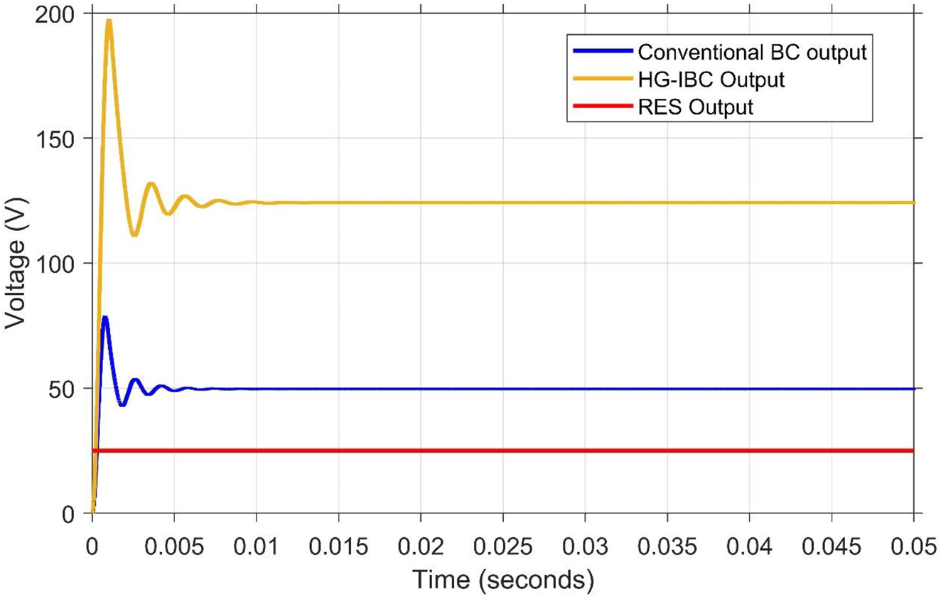
Output voltage of RES and HG-IBC.
The voltage output of RES and HG-IQBC is shown in Figure 24. RES’s V out is 25 V, which is very low. It must be improved for grid-connected modes of operation. The conventional BC output is two times the boost factor, resulting in a total V out of 50 V. This voltage is insufficient for grid integration. So, the HG-IQBC topology is proposed to improve the output by six times, resulting in a V out of 150 V.
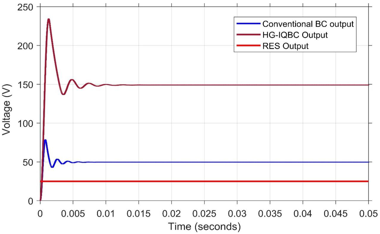
Output voltage of RES and HG-IQBC.
Figure 25 depicts the voltage output of the RES and HG-CBC. RES’s V out is 25 V, which is less. It must be improved for grid-connected modes of operation. The conventional BC output is two times the boost factor, resulting in a V out of 50 V. This voltage is insufficient for grid integration. So, the HG-CBC topology is proposed to improve the output by eight times, resulting in a V out of 200 V.
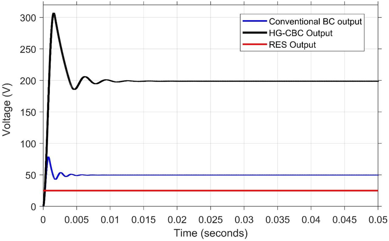
Output voltage of RES and HG-CBC.
9 Conclusions
The goal of this research is to afford a unique, extensive, perceptive, and comparative analysis of various HG-BC configurations for RES and EV applications. The operating principle and mathematical modeling of the HG-QFBC, HG-QBC, HG-IBC, HG-IQBC, and HG-CBC topologies have been reviewed, analyzed, and discussed. For a 0.5 duty cycle, a detailed comparison of various HG-BC is made in terms of B and component count.
Furthermore, for the above-mentioned HG-BC topologies, simulation has been carried out by employing the MATLAB/Simulink tool. The evaluation is done based on theoretical comparisons of performance traits like voltage gain, boost factor, and number of components.
-
Author contributions: All the authors have accepted responsibility for the entire content of this submitted manuscript and approved submission.
-
Research funding: None declared.
-
Conflict of interest statement: The authors declare no conflicts of interest regarding this article.
References
Acar, C., and I. Dincer. 2017. “Environmental Impact Assessment of Renewables and Conventional Fuels for Different End Use Purposes.” International Journal of Global Warming 13 (3–4): 260–77, https://doi.org/10.1504/ijgw.2017.087197.Search in Google Scholar
Ali, M. S., S. K. Kamarudin, M. S. Masdar, and A. Mohamed. 2014. “An Overview of Power Electronics Applications in Fuel Cell Systems: DC and AC Converters.” The Scientific World Journal 2014: 1–9, https://doi.org/10.1155/2014/103709.Search in Google Scholar PubMed PubMed Central
Aihsan, M. Z., M. M. Azizan, M. I. Fahmi, A. M. Yusof, and M. F. Hariz. 2022. “High Gain DC/DC Boost Converter for Electrical Vehicle Applications.” In Proceedings of the 6th International Conference on Electrical, Control and Computer Engineering, 69–78. Singapore: Springer.10.1007/978-981-16-8690-0_7Search in Google Scholar
Ahmad, M., A. Moumin, F. Panhwar, and A. Adam. 2018. High Gain Non-Isolated DC-DC Converter Topologies for Energy Conversion Systems. Doctoral dissertation. Board Bazar, Gazipur: Department of Electrical and Electronic Engineering, Islamic University of Technology.Search in Google Scholar
Ahmad, J., I. Pervez, A. Sarwar, M. Tariq, M. Fahad, R. K. Chakrabortty, and M. J. Ryan. 2020. “Performance Analysis and Hardware-In-The-Loop (HIL) Validation of Single Switch High Voltage gain DC–DC Converters for MPP Tracking in Solar PV System.” IEEE Access 9: 48811–30, https://doi.org/10.1109/access.2020.3034310.Search in Google Scholar
Alghaythi, M. L., R. M. O’Connell, N. E. Islam, M. M. S. Khan, and J. M. Guerrero. 2020. “A High Step-Up Interleaved DC-DC Converter with Voltage Multiplier and Coupled Inductors for Renewable Energy Systems.” IEEE Access 8: 123165–74, https://doi.org/10.1109/access.2020.3007137.Search in Google Scholar
Chandrasekar, B., C. Nallaperumal, S. Padmanaban, M. S. Bhaskar, J. B. Holm-Nielsen, Z. Leonowicz, and S. O. Masebinu. 2020. “Non-isolated High-Gain Triple Port DC–DC Buck-Boost Converter with Positive Output Voltage for Photovoltaic Applications.” IEEE Access 8: 113649–66, https://doi.org/10.1109/access.2020.3003192.Search in Google Scholar
Dawood, N. B. 2016. “Review of Different DC to DC Converters Based for Renewable Energy Applications.” International Research Journal of Engineering and Technology 3 (3): 46–50.Search in Google Scholar
Elsayad, N., H. Moradisizkoohi, and O. Mohammed. 2018. “A New Three-Level Flying-Capacitor Boost Converter with an Integrated LC 2 D Output Network for Fuel-Cell Vehicles: Analysis and Design.” Inventions 3 (3): 61, https://doi.org/10.3390/inventions3030061.Search in Google Scholar
Forouzesh, M., Y. P. Siwakoti, S. A. Gorji, F. Blaabjerg, and B. Lehman. 2017. “Step-up DC–DC Converters: A Comprehensive Review of Voltage-Boosting Techniques, Topologies, and Applications.” IEEE Transactions on Power Electronics 32 (12): 9143–78, https://doi.org/10.1109/tpel.2017.2652318.Search in Google Scholar
Gore, S., P. K. Maroti, M. Al-Hitmi, and A. Iqbal. 2019. “A Dual Output High Gain DC-to-DC Converter for Electric Vehicle Application.” In 2019 International Conference on Power Electronics, Control and Automation (ICPECA), 1–6. New Delhi: IEEE.10.1109/ICPECA47973.2019.8975531Search in Google Scholar
Hasanpour, S., Y. P. Siwakoti, and F. Blaabjerg. 2022. “A New High Efficiency High Step-Up DC/DC Converter for Renewable Energy Applications.” IEEE Transactions on Industrial Electronics 70 (2): 1489–500, https://doi.org/10.1109/tie.2022.3161798.Search in Google Scholar
Hossain, M. Z., and N. A. Rahim. 2018. “Recent Progress and Development on Power DC–DC Converter Topology, Control, Design and Applications: A Review.” Renewable and Sustainable Energy Reviews 81: 205–30, https://doi.org/10.1016/j.rser.2017.07.017.Search in Google Scholar
Hosseini, S. H., R. S. Alishah, and N. V. Kurdkandi. 2015. “Design of a New Extended Zeta Converter with High Voltage Gain for Photovoltaic Applications.” In 2015 9th International Conference on Power Electronics and ECCE Asia (ICPE-ECCE Asia), 970–7. Seoul: IEEE.10.1109/ICPE.2015.7167899Search in Google Scholar
Jagadeesh, I., and V. Indragandhi. 2022. “Comparative Study of DC–DC Converters for Solar PV with Microgrid Applications.” Energies 15 (20): 7569, https://doi.org/10.3390/en15207569.Search in Google Scholar
Kabalo, M., B. Blunier, D. Bouquain, and A. Miraoui. 2010. “State-of-the-Art of DC-DC Converters for Fuel Cell Vehicles.” In 2010 IEEE Vehicle Power and Propulsion Conference, 1–6. Lille: IEEE.10.1109/VPPC.2010.5729051Search in Google Scholar
Keerthana, R., and N. J. Chintu. 2017. “Performance Analysis of Zeta Converter in Wind Power Application.” Asian Journal of Applied Science and Technology 1 (3): 199–203.Search in Google Scholar
Khare, V., S. Nema, and P. Baredar. 2013. “Status of Solar Wind Renewable Energy in India.” Renewable and Sustainable Energy Reviews 27: 1–10, https://doi.org/10.1016/j.rser.2013.06.018.Search in Google Scholar
Kumar, B. M., S. N. Rao, and M. S. Indira. 2022. “Analysis of Grid-Connected Reduced Switch MLI with High-Gain Interleaved Boost Converter and Hybrid MPPT for Solar PV.” International Journal of Energy and Environmental Engineering 1–21, https://doi.org/10.1007/s40095-022-00479-4.Search in Google Scholar
Manikandan, A., and N. Vadivel. 2013. “Design and Implementation of Luo Converter for Electric Vehicle Applications.” International Journal of Engineering Trends and Technology 4 (10): 4437–41.Search in Google Scholar
Mansour, A. S., A. H. H. Amer, E. E. El-Kholy, and M. S. Zaky. 2022. “High Gain DC/DC Converter with Continuous Input Current for Renewable Energy Applications.” Scientific Reports 12 (1): 1–22, https://doi.org/10.1038/s41598-022-16246-8.Search in Google Scholar PubMed PubMed Central
Mansour, A. S., and M. S. Zaky. 2023. “A New Extended Single-Switch High gain DC–DC Boost Converter for Renewable Energy Applications.” Scientific Reports 13 (1): 264, https://doi.org/10.1038/s41598-022-26660-7.Search in Google Scholar PubMed PubMed Central
Maroti, P. K., S. Padmanaban, J. B. Holm-Nielsen, M. S. Bhaskar, M. Meraj, and A. Iqbal. 2019. “A New Structure of High Voltage Gain SEPIC Converter for Renewable Energy Applications.” IEEE Access 7: 89857–68, https://doi.org/10.1109/access.2019.2925564.Search in Google Scholar
Matam, M. B., A. K. D. Venkata, and V. K. Mallapu. 2018. “Analysis and Implementation of Impedance Source Based Switched Capacitor Multi-Level Inverter.” Engineering Science and Technology, An International Journal 21 (5): 869–85, https://doi.org/10.1016/j.jestch.2018.08.003.Search in Google Scholar
Meinagh, F. A. A., V. Ranjbarizad, and E. Babaei. 2019. “New Non-Isolated High Voltage gain Single-Switch DC-DC Converter Based on Voltage-Lift Technique.” In 2019 10th International Power Electronics, Drive Systems and Technologies Conference (PEDSTC), 219–23. Shiraz: IEEE.10.1109/PEDSTC.2019.8697254Search in Google Scholar
Moradpour, R., H. Ardi, and A. Tavakoli. 2017. “Design and Implementation of a New SEPIC-Based High Step-Up DC/DC Converter for Renewable Energy Applications.” IEEE Transactions on Industrial Electronics 65 (2): 1290–7, https://doi.org/10.1109/tie.2017.2733421.Search in Google Scholar
Mumtaz, F., N. Z. Yahaya, S. T. Meraj, B. Singh, R. Kannan, and O. Ibrahim. 2021. “Review on Non-isolated DC–DC Converters and Their Control Techniques for Renewable Energy Applications.” Ain Shams Engineering Journal 12 (4): 3747–63, https://doi.org/10.1016/j.asej.2021.03.022.Search in Google Scholar
Nagaraja Rao, S., S. K. Anisetty, B. M. Manjunatha, B. M. Kiran Kumar, V. Praveen Kumar, and S. Pranupa. 2022. “Interleaved High-Gain Boost Converter Powered by Solar Energy Using Hybrid-Based Mpp Tracking Technique.” Clean Energy 6 (3): 460–75, https://doi.org/10.1093/ce/zkac026.Search in Google Scholar
Naresh, S. V. K., S. Peddapati, and M. L. Alghaythi. 2021. “Non-Isolated High Gain Quadratic Boost Converter Based on Inductor’s Asymmetric Input Voltage.” IEEE Access 9: 162108–21, https://doi.org/10.1109/access.2021.3133581.Search in Google Scholar
Navamani, J. D., A. Lavanya, D. Almakhles, and M. J. Sathik. 2022. “A Review on Segregation of Various High Gain Converter Configurations for Distributed Energy Sources.” Alexandria Engineering Journal 61 (1): 675–700, https://doi.org/10.1016/j.aej.2021.06.026.Search in Google Scholar
Perera, F. 2018. “Pollution from Fossil-Fuel Combustion is the Leading Environmental Threat to Global Pediatric Health and Equity: Solutions Exist.” International Journal of Environmental Research and Public Health 15 (1): 16, https://doi.org/10.3390/ijerph15010016.Search in Google Scholar PubMed PubMed Central
Pranupa, S., A. T. Sriram, and S. Nagaraja Rao. 2022. “Wind energy conversion system using perturb & observe-based maximum power point approach interfaced with T-type three-level inverter connected to grid.” Clean Energy 6 (4): 534–49, https://doi.org/10.1093/ce/zkac034.Search in Google Scholar
Purushothaman, S. K., D. Sattianadan, and K. Vijayakumar. 2022. “Novel Compact Design High gain DC–DC Step Up Converter Applicable for PV Applications.” Sustainable Energy Technologies and Assessments 51: 101720, https://doi.org/10.1016/j.seta.2021.101720.Search in Google Scholar
Radhika, S., and V. Margaret. 2021. “A Review on DC-DC Converters with Photovoltaic System in DC Micro Grid.” In Journal of Physics: Conference Series, Vol. 1804, 1st ed., 012155. IOP Publishing.10.1088/1742-6596/1804/1/012155Search in Google Scholar
Raghavendra, K. V. G., K. Zeb, A. Muthusamy, T. N. V. Krishna, S. V. P. Kumar, D. H. Kim, M. S. Kim, H. G. Cho, and H. J. Kim. 2019. “A Comprehensive Review of DC–DC Converter Topologies and Modulation Strategies with Recent Advances in Solar Photovoltaic Systems.” Electronics 9 (1): 31, https://doi.org/10.3390/electronics9010031.Search in Google Scholar
Rahimi, T., L. Ding, H. Gholizadeh, R. S. Shahrivar, and R. Faraji. 2021. “An Ultra High Step-Up DC–DC Converter Based on the Boost, Luo, and Voltage Doubler Structure: Mathematical Expression, Simulation, and Experimental.” IEEE Access 9: 132011–24, https://doi.org/10.1109/access.2021.3115259.Search in Google Scholar
Rao, S. N., Veerabhadra, and P. Kumar. 2020. “Performance Analysis of Z-Source Inverter Topologies for Renewable Energy Sources and Fuel Cell Applications.” In 2020 IEEE International Conference on Distributed Computing, VLSI, Electrical Circuits and Robotics (DISCOVER), 165–70. Udupi: IEEE.10.1109/DISCOVER50404.2020.9278046Search in Google Scholar
Raveendhra, D., P. Rajana, K. S. R. Kumar, P. Jugge, R. Devarapalli, E. Rusu, and H. H. Fayek. 2022. “A High-Gain Multiphase Interleaved Differential Capacitor Clamped Boost Converter.” Electronics 11 (2): 264, https://doi.org/10.3390/electronics11020264.Search in Google Scholar
Reddy, D. S. 2021. “Review on Power Electronic Boost Converters.” Australian Journal of Electrical and Electronics Engineering 18 (3): 127–37, https://doi.org/10.1080/1448837x.2021.1935091.Search in Google Scholar
Rehman, Z., I. Al-Bahadly, and S. Mukhopadhyay. 2015. “Multiinput DC–DC Converters in Renewable Energy Applications–An Overview.” Renewable and Sustainable Energy Reviews 41: 521–39, https://doi.org/10.1016/j.rser.2014.08.033.Search in Google Scholar
Revathi, B. S., and M. Prabhakar. 2016. “Non Isolated High gain DC–DC Converter Topologies for PV Applications–A Comprehensive Review.” Renewable and Sustainable Energy Reviews 66: 920–33, https://doi.org/10.1016/j.rser.2016.08.057.Search in Google Scholar
Sabzali, A. J., E. H. Ismail, and H. M. Behbehani. 2015. “High Voltage Step-Up Integrated Double Boost–Sepic DC–DC Converter for Fuel-Cell and Photovoltaic Applications.” Renewable Energy 82: 44–53, https://doi.org/10.1016/j.renene.2014.08.034.Search in Google Scholar
Samuel, V. J., G. Keerthi, and P. Mahalingam. 2020. “Non‐Isolated DC–DC Converter with Cubic Voltage gain and Ripple‐Free Input Current.” IET Power Electronics 13 (16): 3675–85, https://doi.org/10.1049/iet-pel.2020.0131.Search in Google Scholar
Shahir, F. M., E. Babaei, and M. Farsadi. 2017. “Voltage-Lift Technique Based Non-Isolated Boost DC–DC Converter: Analysis and Design.” IEEE Transactions on Power Electronics 33: 5917–26.10.1109/TPEL.2017.2740843Search in Google Scholar
Sivakumar, S., M. J. Sathik, P. S. Manoj, and G. Sundararajan. 2016. “An Assessment on Performance of DC–DC Converters for Renewable Energy Applications.” Renewable and Sustainable Energy Reviews 58: 1475–85, https://doi.org/10.1016/j.rser.2015.12.057.Search in Google Scholar
Suryoatmojo, H., R. Mardiyanto, D. C. Riawan, S. Anam, E. Setijadi, S. Ito, and I. Wan. 2018. “Implementation of High Voltage Gain DC–DC Boost Converter for Fuel Cell Application.” In 2018 International Conference on Engineering, Applied Sciences, and Technology (ICEAST), 1–4. Phuket: IEEE.10.1109/ICEAST.2018.8434428Search in Google Scholar
Torkan, A., and M. Ehsani. 2018. “A Novel Nonisolated Z-Source DC–DC Converter for Photovoltaic Applications.” IEEE Transactions on Industry Applications 54 (5): 4574–83, https://doi.org/10.1109/tia.2018.2833821.Search in Google Scholar
Varanasi, P. K., S. Nagaraja Rao, and P Duraiswamy. 2023. “Intelligent Control of Double Boost Converter Interfaced with Multilevel Inverter for Electrical Vehicle Applications.” Journal of The Institution of Engineers (India): Series B, https://doi.org/10.1007/s40031-022-00828-1.Search in Google Scholar
Veerabhadra, and S Nagaraja Rao. 2022. “Assessment of High-Gain Quadratic Boost Converter with Hybrid-Based Maximum Power Point Tracking Technique for Solar Photovoltaic Systems.” Clean Energy 6 (4): 632–45, https://doi.org/10.1093/ce/zkac041.Search in Google Scholar
Veerachary, M., and N. Kumar. 2020. “Analysis and Design of Quadratic Following Boost Converter.” IEEE Transactions on Industry Applications 56 (6): 6657–73, https://doi.org/10.1109/tia.2020.3021363.Search in Google Scholar
Wu, B., S. Li, Y. Liu, and K. M. Smedley. 2015. “A New Hybrid Boosting Converter for Renewable Energy Applications.” IEEE Transactions on Power Electronics 31 (2): 1203–15, https://doi.org/10.1109/tpel.2015.2420994.Search in Google Scholar
Zaid, M., C. H. Lin, S. Khan, J. Ahmad, M. Tariq, A. Mahmood, A. Sarwar, B. Alamri, and A. Alahmadi. 2021. “A Family of Transformerless Quadratic Boost High Gain DC–DC Converters.” Energies 14 (14): 4372, https://doi.org/10.3390/en14144372.Search in Google Scholar
Zaid, M., I. H. Malick, I. Ashraf, M. Tariq, B. Alamri, and E. M. Rodrigues. 2022. “A Nonisolated Transformerless High-Gain DC–DC Converter for Renewable Energy Applications.” Electronics 11 (13): 2014, https://doi.org/10.3390/electronics11132014.Search in Google Scholar
Zhang, N., D. Sutanto, and K. M. Muttaqi. 2016. “A Review of Topologies of Three-Port DC–DC Converters for the Integration of Renewable Energy and Energy Storage System.” Renewable and Sustainable Energy Reviews 56: 388–401, https://doi.org/10.1016/j.rser.2015.11.079.Search in Google Scholar
© 2024 the author(s), published by De Gruyter, Berlin/Boston
This work is licensed under the Creative Commons Attribution 4.0 International License.
Articles in the same Issue
- Solar photovoltaic-integrated energy storage system with a power electronic interface for operating a brushless DC drive-coupled agricultural load
- Analysis of 1-year energy data of a 5 kW and a 122 kW rooftop photovoltaic installation in Dhaka
- Reviews
- Real yields and PVSYST simulations: comparative analysis based on four photovoltaic installations at Ibn Tofail University
- A comprehensive approach of evolving electric vehicles (EVs) to attribute “green self-generation” – a review
- Exploring the piezoelectric porous polymers for energy harvesting: a review
- A strategic review: the role of commercially available tools for planning, modelling, optimization, and performance measurement of photovoltaic systems
- Comparative assessment of high gain boost converters for renewable energy sources and electrical vehicle applications
- A review of green hydrogen production based on solar energy; techniques and methods
- A review of green hydrogen production by renewable resources
- A review of hydrogen production from bio-energy, technologies and assessments
- A systematic review of recent developments in IoT-based demand side management for PV power generation
- Research Articles
- Hybrid optimization strategy for water cooling system: enhancement of photovoltaic panels performance
- Solar energy harvesting-based built-in backpack charger
- A power source for E-devices based on green energy
- Theoretical and experimental investigation of electricity generation through footstep tiles
- Experimental investigations on heat transfer enhancement in a double pipe heat exchanger using hybrid nanofluids
- Comparative energy and exergy analysis of a CPV/T system based on linear Fresnel reflectors
- Investigating the effect of green composite back sheet materials on solar panel output voltage harvesting for better sustainable energy performance
- Electrical and thermal modeling of battery cell grouping for analyzing battery pack efficiency and temperature
- Intelligent techno-economical optimization with demand side management in microgrid using improved sandpiper optimization algorithm
- Investigation of KAPTON–PDMS triboelectric nanogenerator considering the edge-effect capacitor
- Design of a novel hybrid soft computing model for passive components selection in multiple load Zeta converter topologies of solar PV energy system
- A novel mechatronic absorber of vibration energy in the chimney
- An IoT-based intelligent smart energy monitoring system for solar PV power generation
- Large-scale green hydrogen production using alkaline water electrolysis based on seasonal solar radiation
- Evaluation of performances in DI Diesel engine with different split injection timings
- Optimized power flow management based on Harris Hawks optimization for an islanded DC microgrid
- Experimental investigation of heat transfer characteristics for a shell and tube heat exchanger
- Fuzzy induced controller for optimal power quality improvement with PVA connected UPQC
- Impact of using a predictive neural network of multi-term zenith angle function on energy management of solar-harvesting sensor nodes
- An analytical study of wireless power transmission system with metamaterials
- Hydrogen energy horizon: balancing opportunities and challenges
- Development of renewable energy-based power system for the irrigation support: case studies
- Maximum power point tracking techniques using improved incremental conductance and particle swarm optimizer for solar power generation systems
- Experimental and numerical study on energy harvesting performance thermoelectric generator applied to a screw compressor
- Study on the effectiveness of a solar cell with a holographic concentrator
- Non-transient optimum design of nonlinear electromagnetic vibration-based energy harvester using homotopy perturbation method
- Industrial gas turbine performance prediction and improvement – a case study
- An electric-field high energy harvester from medium or high voltage power line with parallel line
- FPGA based telecommand system for balloon-borne scientific payloads
- Improved design of advanced controller for a step up converter used in photovoltaic system
- Techno-economic assessment of battery storage with photovoltaics for maximum self-consumption
- Analysis of 1-year energy data of a 5 kW and a 122 kW rooftop photovoltaic installation in Dhaka
- Shading impact on the electricity generated by a photovoltaic installation using “Solar Shadow-Mask”
- Investigations on the performance of bottle blade overshot water wheel in very low head resources for pico hydropower
- Solar photovoltaic-integrated energy storage system with a power electronic interface for operating a brushless DC drive-coupled agricultural load
- Numerical investigation of smart material-based structures for vibration energy-harvesting applications
- A system-level study of indoor light energy harvesting integrating commercially available power management circuitry
- Enhancing the wireless power transfer system performance and output voltage of electric scooters
- Harvesting energy from a soldier's gait using the piezoelectric effect
- Study of technical means for heat generation, its application, flow control, and conversion of other types of energy into thermal energy
- Theoretical analysis of piezoceramic ultrasonic energy harvester applicable in biomedical implanted devices
- Corrigendum
- Corrigendum to: A numerical investigation of optimum angles for solar energy receivers in the eastern part of Algeria
- Special Issue: Recent Trends in Renewable Energy Conversion and Storage Materials for Hybrid Transportation Systems
- Typical fault prediction method for wind turbines based on an improved stacked autoencoder network
- Power data integrity verification method based on chameleon authentication tree algorithm and missing tendency value
- Fault diagnosis of automobile drive based on a novel deep neural network
- Research on the development and intelligent application of power environmental protection platform based on big data
- Diffusion induced thermal effect and stress in layered Li(Ni0.6Mn0.2Co0.2)O2 cathode materials for button lithium-ion battery electrode plates
- Improving power plant technology to increase energy efficiency of autonomous consumers using geothermal sources
- Energy-saving analysis of desalination equipment based on a machine-learning sequence modeling