
Adjoint-optimized nanoscale light extractor for nitrogen-vacancy centers in diamond
-
Raymond A. Wambold
 ,
Zhaoning Yu
,
Yuzhe Xiao
,
Benjamin Bachman
,
Gabriel Jaffe
,
Shimon Kolkowitz
,
Jennifer T. Choy
,
Mark A. Eriksson
,
Robert J. Hamers
and
Mikhail A. Kats
,
Zhaoning Yu
,
Yuzhe Xiao
,
Benjamin Bachman
,
Gabriel Jaffe
,
Shimon Kolkowitz
,
Jennifer T. Choy
,
Mark A. Eriksson
,
Robert J. Hamers
and
Mikhail A. Kats


Abstract
We designed a nanoscale light extractor (NLE) for the efficient outcoupling and beaming of broadband light emitted by shallow, negatively charged nitrogen-vacancy (NV) centers in bulk diamond. The NLE consists of a patterned silicon layer on diamond and requires no etching of the diamond surface. Our design process is based on adjoint optimization using broadband time-domain simulations and yields structures that are inherently robust to positioning and fabrication errors. Our NLE functions like a transmission antenna for the NV center, enhancing the optical power extracted from an NV center positioned 10 nm below the diamond surface by a factor of more than 35, and beaming the light into a ±30° cone in the far field. This approach to light extraction can be readily adapted to other solid-state color centers.
1 Introduction
Negatively charged nitrogen-vacancy (NV) centers in diamond are optical emitters whose level structure is highly sensitive to external perturbations, which makes them excellent sensors of highly localized electric and magnetic fields, temperature, and strain [1], [2], [3], [4], [5]. NV centers are of great interest for quantum computing and communication [6], [7], [8], [9], [10] and the study of quantum phenomena such as quantum entanglement and superposition [11], [, 12]. However, efficiently extracting NV fluorescence is often challenging due to the high index of refraction in diamond (∼2.4), which results in high reflectance at the diamond–air interfaces and total internal reflection for emission angles larger than the critical angle. Previous attempts to extract more light from bulk diamond primarily involved the etching of the diamond itself (a complicated fabrication process that can adversely affect NV properties such as spin coherence) [13], [14], [15], [16], [17], [18], [19] or fabricating structures that still required a high-numerical-aperture oil-immersion objective to efficiently collect the emission (which adds system complexity and is detrimental to sensing applications) [20], [21], [22], [23]. Furthermore, precision etching of diamond around NV centers can be a substantial challenge and can damage the surface of diamond, resulting in roughness and modification of the chemical termination [24], which can degrade the quantum properties of NV centers [25], [, 26].
Here, we design a silicon-based nanoscale light extractor (NLE) that sits on the top of a flat, unpatterned diamond surface and can enhance the optical output of near-surface NV emitters by more than 35× compared with the unpatterned case, directing the light into a narrow cone that can be easily collected with low-NA optical systems. Our NLE consists of a patterned silicon structure on top of the diamond surface (Figure 1), directly above a shallow NV center (<300 nm below the surface). The proximity of a resonant high-index dielectric structure close to the emitter enables near-field coupling to and broadband Purcell enhancement of the emitter [23], [, 27]. We designed the silicon NLE using an adjoint-optimization method, optimizing for NV emission funneled into a narrow cone into the far field. This approach both increases collection efficiency and enhances the radiative emission rate of the NV center.
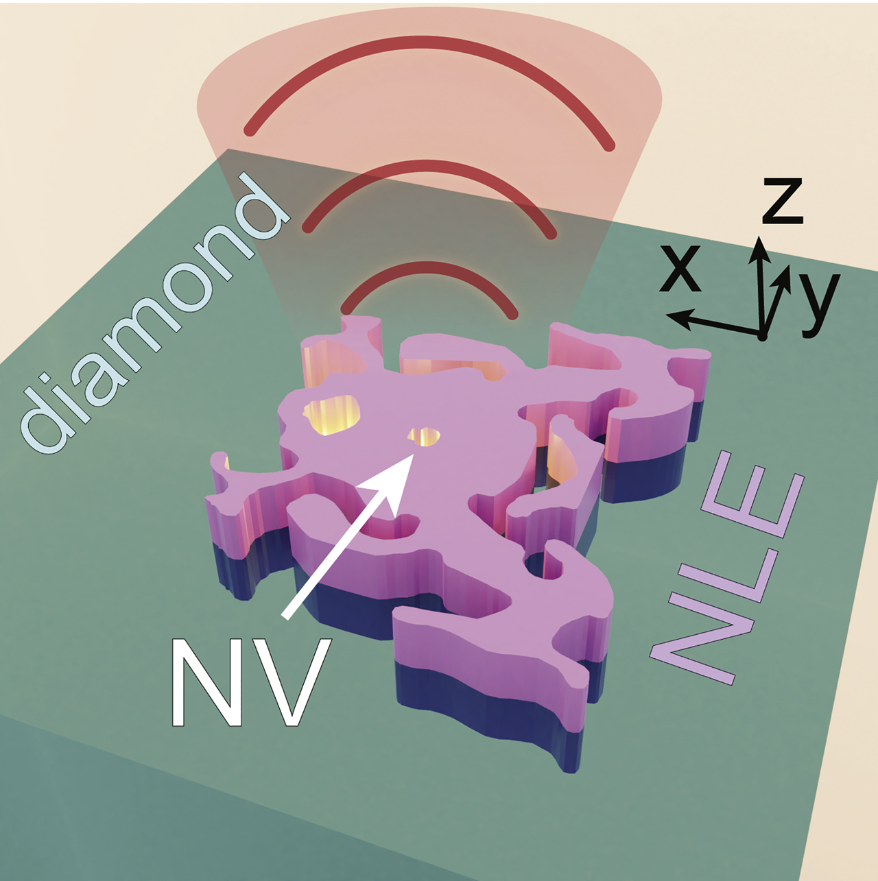
Schematic of the nanoscale light extractor (NLE), which sits on the diamond surface above a nitrogen-vacancy (NV) center and directs fluorescence out of the diamond and into a narrow cone in the far field.
The schematic is a render of the actual optimized structure reported below.
Our approach focuses on broadband emission enhancement of negatively charged NV centers close to the diamond surface, which is especially useful for sensing applications in which measurement sensitivity is limited by the number of collected photons across the entire NV emission spectrum.
2 Figure of merit for broadband NV emission extraction
We targeted our design toward negatively charged NV centers in [100] diamond. The NV axis is at an angle of 54.7° with respect to the normal to the diamond surface in this orientation [28], and the optical dipole moments are orthogonal to the NV axis [29]. At room temperature, the emission from an NV center is expected to be unpolarized [30] and can therefore be simulated by the incoherent sum of emitted intensities from any two orthogonal linear dipoles that are also orthogonal to the NV axis. In bulk diamond, negatively charged NV centers have optical transitions at ∼637 nm (the location of the zero-phonon line in the spectrum), but fluoresce over a bandwidth of >150 nm due to vibrational side bands in the diamond [28], [, 31]. Therefore, we define a spectrum-averaged figure of merit (FoM) to quantify the degree of light extraction:
Here,
For all plots in this paper, the bounds of the integral in Eq. (1) are set to 635–800 nm to cover the NV zero-phonon line and phonon sideband emission spectrum. Our NLE achieves broadband NV fluorescence enhancement, which is particularly useful for sensing applications using shallow NVs, but the design approach can readily be adapted to focus on more-narrow spectral ranges (e.g., the zero-phonon line alone).
3 Adjoint-optimization method
To design a high-performance NLE, we used adjoint optimization—a design technique that has been used extensively in mechanical engineering and has recently been applied to the design of optical metasurfaces and other photonic structures [33], [34], [35]. For free-form structures that are allowed to evolve in three dimensions, the optimization process consists of the evolution of the structure, defined by a refractive-index profile
Owing to the incoherent and unpolarized emission pattern of the NV center at room temperature, our approach was to maximize extraction from two orthogonal optical-dipole orientations [29]. We used two pairs of forward/adjoint simulations for these two orientations. The first of our forward simulations is sourced by an electric dipole 10 nm below the diamond surface, with the dipole moment oriented in the XZ plane and tilted at an angle of 35.3° off the Z axis. The second was sourced by a dipole placed at the same position and oriented parallel to the Y axis. Note that NV centers in [100] diamond can be oriented in one of four directions along the ⟨111⟩ crystal axes. Thus to maximize performance, prior characterization can be done to align the NLE in the proper direction during fabrication [36]. Two adjoint Gaussian beams were used with orthogonal polarizations; one polarized along the X axis and the other polarized along the Y axis to pair with the forward dipoles in the XZ plane and along the Y axis, respectively.
We used finite-difference time-domain (FDTD) simulations (implemented in Lumerical FDTD [37]) to determine the forward and adjoint fields in the optimization region across the spectrum of interest for both optimization pairs. At each optimization generation, we calculated a figure-of-merit gradient similar to that of Ref. [38], but averaged across the forward/adjoint simulation pairs:
For the case of only one forward/adjoint pair, a positive value of
To design a structure that can realistically be fabricated using top-down techniques, there should ideally be no material variance in the vertical (Z) direction. We impose this constraint in our optimization by 1) forcing the index in a single column along Z to be constant, and 2) averaging
(similar to, e.g., Ref. [38]), where
Figure 2(A) shows the design process for our NLE. To start, the optimization is seeded with a random continuous distribution of complex refractive index, taking values between that of air
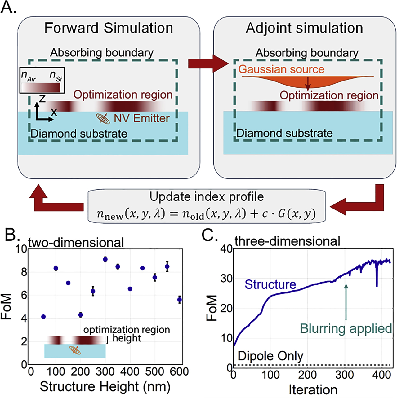
(A) Visualization of the optimization routine, which evolves an index profile situated above an NV emitter. In the forward simulation, the light source is a dipole at the location of the NV. The sources in the adjoint simulations are two orthogonally polarized Gaussian beams injected from free space toward the structure. The sensitivity gradient,
However, the optimization method described above yields an optimized profile
where
In addition to blurring, a binary push function is required to finish the optimization with a fully binary structure (i.e., in our case, at each point in the optimization region the final material should be either air or silicon). The binarization method found in Refs. [40] and [35] was the guide for our implementation. Specifically, this method modifies the blurred element matrix as follows:
where
We leveraged the inherently broadband nature of the FDTD method to simulate and optimize the performance of our device across the entire NV emission spectrum, simultaneously achieving a design that is robust to errors in fabrication. Previous works using adjoint optimization with a frequency-domain electromagnetic solver achieve fabrication robustness through simulating dilated and eroded devices each iteration, which corresponds to a three-fold increase in the number of simulations required [34], [35], [41], [42]. In our optimizations, fabrication robustness was built-in automatically due to our requirement for broadband performance together with the scale invariance of Maxwell’s equations (i.e., larger structures at longer wavelengths behave similarly to smaller structures at shorter wavelengths). This correspondence between broadband performance and shape robustness has been observed previously for other inverse-design approaches [43], [, 44].
Note that our adjoint optimization setup that uses
4 Designing the nanoscale light extractor
To find the ideal height, we first ran a series of a series of 2D optimizations, sweeping over a range of heights of the NLE [Figure 2(A and B)]. Like in the later 3D simulations, the 2D simulations were set up with the dipole embedded 10 nm into diamond, and we used two orthogonal dipole orientations in a plane perpendicular to the NV axis. We swept the NLE height from 50 to 600 nm in steps of 50 nm and ran five optimization runs for each height. Figure 2(B) shows the average of our FoM for each height, with the oscillations reminiscent of Fabry–Perot fringes. Based on these results, we decided to run the full 3D optimization of the NLE for a height of 300 nm. This thickness is a common device-layer thickness in silicon-on-insulator (SOI) technology [45] and we note that SOI lends itself well to fabricating this structure as crystalline silicon device layers can be transferred to diamond using membrane-transfer techniques [46].
The full 3D optimization run can be seen in Figure 2(C). The FoM increases as the optimization progresses, with occasional dips due to the implementation of the secondary blurring function. The optimization terminates when the device is sufficiently binarized, such that the structure is entirely comprised of air and silicon, and the FoM is no longer improving significantly.
5 Results
The structure of our optimized NLE is shown in Figure 3(A), with the extraction efficiency in Figure 3(B). Although the NLE was optimized for an NV depth of 10 nm, we also show the results for depths of 5 and 15 nm but with the same NLE structure. The extraction efficiency increases for NVs closer to the structure due to increased coupling with the NLE, which leads to larger Purcell enhancement [47]. For an NV depth of 10 nm, the Purcell enhancement of our device is ∼3, averaged across the emission spectrum. Here, we calculate the Purcell enhancement by dividing the power emitted by the dipole source in the presence of the interface and the NLE by the power emitted by the dipole in homogeneous diamond (no interface).
![Figure 3: (A) Top-down view of the final NLE optimized for an NV depth of 10 nm. (B) Extraction efficiency [η(λ)]$\left[\eta \left(\lambda \right)\right]$ of the NLE for NV depths of 5, 10, and 15 nm below the diamond/air interface. (C and D) Snapshot of the near and meso- fields of the emitted electric field from (left) a dipole in the X–Z plane, and (right) a dipole in the Y direction. (D) Intensity far-field averaged over the two dipole orientations. In C and D, the plots are at a wavelength of 675 nm. The bulk of the beamed power fits within a 60° cone in the far field. NLE, nanoscale light extractor; NV, nitrogen-vacancy.](/document/doi/10.1515/nanoph-2020-0387/asset/graphic/j_nanoph-2020-0387_fig_003.jpg)
(A) Top-down view of the final NLE optimized for an NV depth of 10 nm. (B) Extraction efficiency
Figure 3(C and D) shows the near- and far-field radiation patterns. The NLE can shape the emitted fields from the dipole into a beam that is approximately Gaussian. The beam angle is slightly offset from the normal (∼7.5°) but the bulk of the beamed power fits within a ±30° cone. The fields in Figure 3(C and D) are for a wavelength of 675 nm, but the beaming persists across the NV spectrum and the peak emission angle does not deviate by more than
Owing to the broadband spectrum incorporated into the optimization, our devices display considerable tolerance to various fabrication defects as well as robustness to alignment errors (Figure 4). Although our optimized NLE structure was based on a fixed NV depth of 10 nm, we also simulated its performance for a variety of depths [Figure 4(A)]. The NLE performs better as the dipole gets closer to the surface because of enhanced near-field coupling. The performance falls off by a factor of 2 at a depth of 40 nm, yet still maintains enhancements of about 15 times the emission of an NV with no NLE. Even down to a dipole depth of 300 nm, the NLE is able to increase the output of the NV by a factor of 3. Note that for NVs at depths substantially different than 10 nm, a more-effective design can very likely be found using the optimization method described previously.

(A) The NLE maintains good performance through a range of depths, with increasing FoM for NVs closer to the surface. (B) FoM dependence on the NV emitter angle emulating angular alignment errors of the NLE. (C) Demonstration of the fabrication robustness of the optimized device for an NV depth of 10 nm. Eroded and dilated structures are based on the optimized structure with edge deviation of ±20 nm to represent fabrication under/over-etching, respectively. Owing to the broadband nature of our optimization, the NLE shows strong tolerance to fabrication errors. (D) Tolerance of the NLE to lateral offsets of the NV center. The FoM remains above 25 for X offsets of ±30 nm and Y offsets of ±40 nm. (e) The geometries of the eroded, optimized, and dilated devices simulated in c. The edge deviation refers to how far the edges shifted inward for the eroded or outward for the dilated cases. FoM, figure of merit; NLE, nanoscale light extractor; NV, nitrogen-vacancy.
The NLE shows minimal performance loss from errors in rotational alignment in the range of −20° to +20° [Figure 4(B)]. The full 360° rotational plot can be found in the Supplementary Material. We also tested the case where the NLE was offset by some amount from the central dipole position [Figure 4(D)], and found that the FoM remains above 25 for X offsets of ±30 nm and Y offsets of ±40 nm.
In practice, one can reasonably expect the fabrication process to cause deviations in edge locations, e.g., due to proximity effects in lithography [48]. Figure 4(C) shows the extraction efficiency of our eroded, optimized, and dilated structures with their index profiles shown in Figure 4(E). We calculated the deviated structures by applying a gaussian blurring filter across the optimized pattern, and then selecting cutoff points of the blurred edges to yield new binarized structures. Here, we selected the blur and cutoff to yield edge deviations of ±20 nm. The NLE maintains good performance across the spectrum despite erosion or dilation [Figure 2(B)].
It is instructive to compare the FoM of our NLE (∼35 for NVs at a depth of 10 nm) with some existing structures in the literature designed for broadband vertical outcoupling of light from a diamond slab, with the understanding that the FoM combines the distinct collection-enhancement and Purcell mechanisms. Dielectric structures comprising etched diamond typically do not provide much Purcell enhancement and include bullseye gratings [21], vertical nanowires [49], solid-immersion metalenses [19], and parabolic reflectors [13]; we estimate that these structures have calculated FoMs of approximately 10–20 due entirely to collection enhancement. Resonant geometries proposed thus far have primarily relied on plasmonic enhancement in structures such as metallic cavities [14], [, 50] and gratings [51], with FoMs of up to ∼35. The theoretical FoM of resonant metal-dielectric structures in Ref. [52] can be well above 100 due to large Purcell enhancement, but the implementation would require elaborate fabrication including filling etched diamond apertures with metal, and the small mode volume limits the positioning tolerance of the NV center to within ∼5 nm of the field maximum. Finally, note that unlike all of the aforementioned designs, our NLE does not require etching of the diamond, and can be fabricated by using Si membrane transfer techniques [46], [, 53] or direct CVD growth of Si on a diamond substrate. We do note that the exact effects of the NLE on the NV-center spin characteristics (e.g., coherence) due to the proximity of the NV to the NLE surface and material are unknown at this time. These effects are difficult to predict and are beyond the scope of this article, warranting future experimental investigations. However, our technique is likely to be less invasive than approaches that require etching the diamond near the NV, which inevitably introduces damage and additional defects.
We note that while the present article was undergoing peer review, a preprint by Chakravarthi et al. describing a similar approach to extracting light for NV centers, but for quantum information applications, was posted on arXiv [54].
6 Conclusion
We presented an NLE designed using adjoint-optimization methods with time-domain simulations to enhance the broadband emission of NV centers in diamond. Our design not only enhances the fluorescence of the NV centers but also demonstrates exceptional beam-shaping qualities, enabling efficient collection with a low-NA lens in free space. Even given reasonable uncertainty in NV center localization and errors in device fabrication, simulations show the NLE maintains a high extraction efficiency. Our results suggest that such robustness to positioning and fabrication errors can be automatically achieved when optimizing for a broadband figure of merit. The NLE can be fabricated with conventional electron-beam lithography techniques without etching of the diamond surface. Our approach can easily be extended to other color centers in diamond, as well as material systems where increased light extraction from defect centers is desired, such as silicon carbide or hexagonal boron nitride [55], [, 56].
Funding source: National Science Foundation
Award Identifier / Grant number: CHE-1839174
Funding source: U.S. Department of Energy
Award Identifier / Grant number: DE-SC0020313
Funding source: Directed Energy Professional Society
Acknowledgments
The authors thank Jad Salman for useful discussions, and also an anonymous reviewer for identifying an error in the orientation of the NV optical axis in a previous version of the manuscript.
Author contribution: All the authors have accepted responsibility for the entire content of this submitted manuscript and approved submission.
Research funding: This material is based upon work supported by the National Science Foundation under Grant No. CHE-1839174. RW acknowledges support through the DoD SMART program and a scholarship from the Directed Energy Professional Society. Additional contributions by JTC and SK were supported by the U.S. Department of Energy (DOE), Office of Science, Basic Energy Sciences (BES) under Award #DE-SC0020313.
Conflict of interest statement: The authors declare no conflicts of interest regarding this article.
References
[1] F. Jelezko and J. Wrachtrup, “Single defect centres in diamond: a review,” Phys. Status Solidi A, vol. 203, no. 13, pp. 3207–3225, 2006, https://doi.org/10.1002/pssa.200671403.Search in Google Scholar
[2] R. Schirhagl, K. Chang, M. Loretz, and C. L. Degen, “Nitrogen-vacancy centers in diamond: nanoscale sensors for physics and biology,” Annu. Rev. Phys. Chem., vol. 65, no. 1, pp. 83–105, 2014, https://doi.org/10.1146/annurev-physchem-040513-103659.Search in Google Scholar
[3] I. Aharonovich and E. Neu, “Diamond nanophotonics,” Adv. Opt. Mater., vol. 2, no. 10, pp. 911–928, 2014, https://doi.org/10.1002/adom.201400189.Search in Google Scholar
[4] L. Rondin, J.-P. Tetienne, T. Hingant, J.-F. Roch, P. Maletinsky, and V. Jacques, “Magnetometry with nitrogen-vacancy defects in diamond,” Rep. Prog. Phys., vol. 77, no. 5, p. 056503, 2014, https://doi.org/10.1088/0034-4885/77/5/056503.Search in Google Scholar
[5] J. F. Barry, J. M. Schloss, E. Bauch, et al.., “Sensitivity optimization for NV-diamond magnetometry,” Rev. Mod. Phys., vol. 92, no. 1, p. 015004, 2020, https://doi.org/10.1103/RevModPhys.92.015004.Search in Google Scholar
[6] L. Childress and R. Hanson, “Diamond NV centers for quantum computing and quantum networks,” MRS Bull., vol. 38, no. 2. Cambridge University Press, pp. 134–138, 2013, https://doi.org/10.1557/mrs.2013.20.Search in Google Scholar
[7] A. Russo, E. Barnes, and S. E. Economou, “Photonic graph state generation from quantum dots and color centers for quantum communications,” Phys. Rev. B, vol. 98, no. 8, p. 085303, 2018, https://doi.org/10.1103/PhysRevB.98.085303.Search in Google Scholar
[8] A. Beveratos, R. Brouri, T. Gacoin, A. Villing, J. P. Poizat, and P. Grangier, “Single photon quantum cryptography,” Phys. Rev. Lett., vol. 89, no. 18, p. 187901, 2002, https://doi.org/10.1103/PhysRevLett.89.187901.Search in Google Scholar
[9] F. Jelezko, T. Gaebel, I. Popa, M. Domhan, A. Gruber, and J. Wrachtrup, “Observation of coherent oscillation of a single nuclear spin and realization of a two-qubit conditional quantum gate,” Phys. Rev. Lett., vol. 93, no. 13, p. 130501, 2004, https://doi.org/10.1103/PhysRevLett.93.130501.Search in Google Scholar
[10] M. V. Gurudev Dutt, L. Childress, L. Jiang, et al.., “Quantum register based on individual electronic and nuclear spin qubits in diamond,” Science, vol. 316, no. 5829, pp. 1312–1316, 2007, https://doi.org/10.1126/science.1139831.Search in Google Scholar
[11] B.-C. Ren and F.-G. Deng, “Hyperentanglement purification and concentration assisted by diamond NV centers inside photonic crystal cavities,” Laser Phys. Lett., vol. 10, no. 11, p. 115201, 2013, https://doi.org/10.1088/1612-2011/10/11/115201.Search in Google Scholar
[12] K. Fang, V. M. Acosta, C. Santori, et al.., “High-sensitivity magnetometry based on quantum beats in diamond nitrogen-vacancy centers,” Phys. Rev. Lett., vol. 110, no. 13, p. 130802, 2013, https://doi.org/10.1103/PhysRevLett.110.130802.Search in Google Scholar
[13] N. H. Wan, B. J. Shields, D. Kim, et al.., “Efficient extraction of light from a nitrogen-vacancy center in a diamond parabolic reflector,” Nano Lett., vol. 18, no. 5, pp. 2787–2793, 2018, https://doi.org/10.1021/acs.nanolett.7b04684.Search in Google Scholar
[14] J. T. Choy, B. J. M. Hausmann, T. M. Babinec, et al.., “Enhanced single-photon emission from a diamond–silver aperture,” Nat. Photonics, vol. 5, no. 12, pp. 738–743, 2011, https://doi.org/10.1038/nphoton.2011.249.Search in Google Scholar
[15] T. Schröder, F. Gädeke, M. J. Banholzer, and O. Benson, “Ultrabright and efficient single-photon generation based on nitrogen-vacancy centres in nanodiamonds on a solid immersion lens,” New J. Phys., vol. 13, 2011, https://doi.org/10.1088/1367-2630/13/5/055017.Search in Google Scholar
[16] P. Siyushev, F. Kaiser, V. Jacques, et al.., “Monolithic diamond optics for single photon detection,” Appl. Phys. Lett., vol. 97, no. 24, p. 241902, 2010, https://doi.org/10.1063/1.3519849.Search in Google Scholar
[17] A. Faraon, P. E. Barclay, C. Santori, K.-M. C. Fu, and R. G. Beausoleil, “Resonant enhancement of the zero-phonon emission from a colour centre in a diamond cavity,” Nat. Photonics, vol. 5, no. 5, pp. 301–305, 2011, https://doi.org/10.1038/nphoton.2011.52.Search in Google Scholar
[18] J. P. Hadden, J. P. Harrison, A. C. Stanley-Clarke, et al.., “Strongly enhanced photon collection from diamond defect centers under microfabricated integrated solid immersion lenses,” Appl. Phys. Lett., vol. 97, no. 24, p. 241901, 2010, https://doi.org/10.1063/1.3519847.Search in Google Scholar
[19] T.-Y. Huang, R. R. Grote, S. A. Mann, et al.., “A monolithic immersion metalens for imaging solid-state quantum emitters,” Nat. Commun., vol. 10, no. 1, p. 2392, 2019, https://doi.org/10.1038/s41467-019-10238-5.Search in Google Scholar
[20] J. Zheng, A. C. Liapis, E. H. Chen, C. T. Black, and D. Englund, “Chirped circular dielectric gratings for near-unity collection efficiency from quantum emitters in bulk diamond,” Opt. Express, vol. 25, no. 26, p. 32420, 2017, https://doi.org/10.1364/oe.25.032420.Search in Google Scholar
[21] L. Li, E. H. Chen, J. Zheng, et al.., “Efficient photon collection from a nitrogen vacancy center in a circular bullseye grating,” Nano Lett., vol. 15, no. 3, pp. 1493–1497, 2015, https://doi.org/10.1021/nl503451j.Search in Google Scholar
[22] S. Schietinger, M. Barth, T. Aichele, and O. Benson, “Plasmon-enhanced single photon emission from a nanoassembled metal–diamond hybrid structure at room temperature,” Nano Lett., vol. 9, no. 4, pp. 1694–1698, 2009, https://doi.org/10.1021/nl900384c.Search in Google Scholar
[23] M. Y. Shalaginov, V. V. Vorobyov, J. Liu, et al.., “Enhancement of single-photon emission from nitrogen-vacancy centers with TiN/(Al,Sc)N hyperbolic metamaterial,” Laser Photonics Rev., vol. 9, no. 1, pp. 120–127, 2015, https://doi.org/10.1002/lpor.201400185.Search in Google Scholar
[24] P. Latawiec, M. J. Burek, Y.-I. Sohn, and M. Lončar, “Faraday cage angled-etching of nanostructures in bulk dielectrics,” J. Vac. Sci. Technol. B Nanotechnol. Microelectron. Mater. Process. Meas. Phenom., vol. 34, no. 4, p. 041801, 2016, https://doi.org/10.1116/1.4944854.Search in Google Scholar
[25] S. Sangtawesin, B. L. Dwyer, S. Srinivasan, et al.., “Origins of diamond surface noise probed by correlating single-spin measurements with surface spectroscopy,” Phys. Rev. X, vol. 9, no. 3, p. 031052, 2019, https://doi.org/10.1103/PhysRevX.9.031052.Search in Google Scholar
[26] M. Kaviani, P. Deák, B. Aradi, T. Frauenheim, J. P. Chou, and A. Gali, “Proper surface termination for luminescent near-surface NV centers in diamond,” Nano Lett., vol. 14, no. 8, pp. 4772–4777, 2014, https://doi.org/10.1021/nl501927y.Search in Google Scholar
[27] J. Riedrich-Möller, S. Pezzagna, J. Meijer, et al.., “Nanoimplantation and Purcell enhancement of single nitrogen-vacancy centers in photonic crystal cavities in diamond,” Appl. Phys. Lett., vol. 106, no. 22, p. 221103, 2015, https://doi.org/10.1063/1.4922117.Search in Google Scholar
[28] M. W. Doherty, N. B. Manson, P. Delaney, F. Jelezko, J. Wrachtrup, and L. C. L. Hollenberg, “The nitrogen-vacancy colour centre in diamond,” Phys. Rep., vol. 528, no. 1. North-Holland, pp. 1–45, 2013, https://doi.org/10.1016/j.physrep.2013.02.001.Search in Google Scholar
[29] R. J. Epstein, F. M. Mendoza, Y. K. Kato, and D. D. Awschalom, “Anisotropic interactions of a single spin and dark-spin spectroscopy in diamond,” Nat. Phys., vol. 1, no. 2, pp. 94–98, 2005, https://doi.org/10.1038/nphys141.Search in Google Scholar
[30] N. Abe, Y. Mitsumori, M. Sadgrove, and K. Edamatsu, “Dynamically unpolarized single-photon source in diamond with intrinsic randomness,” Sci. Rep., vol. 7, no. 1, p. 1, 2017, https://doi.org/10.1038/srep46722.Search in Google Scholar
[31] N. B. Manson and J. P. Harrison, “Photo-ionization of the nitrogen-vacancy center in diamond,” Diam. Relat. Mater., vol. 14, no. 10, pp. 1705–1710, 2005, https://doi.org/10.1016/j.diamond.2005.06.027.Search in Google Scholar
[32] R. Albrecht, A. Bommer, C. Deutsch, J. Reichel, and C. Becher, “Coupling of a single nitrogen-vacancy center in diamond to a fiber-based microcavity,” Phys. Rev. Lett., vol. 110, no. 24, p. 243602, 2013, https://doi.org/10.1103/PhysRevLett.110.243602.Search in Google Scholar
[33] J. S. Jensen and O. Sigmund, “Topology optimization for nano-photonics,” Laser Photonics Rev., vol. 5, no. 2, pp. 308–321, 2011, https://doi.org/10.1002/lpor.201000014.Search in Google Scholar
[34] D. Sell, J. Yang, S. Doshay, R. Yang, and J. A. Fan, “Large-angle, multifunctional metagratings based on freeform multimode geometries,” Nano Lett., vol. 17, no. 6, pp. 3752–3757, 2017, https://doi.org/10.1021/acs.nanolett.7b01082.Search in Google Scholar
[35] E. W Wang, D Sell, T Phan, and J. A Fan. “Robust design of topology-optimized metasurfaces,” Opt. Mater. Express, vol. 9, no. 2, pp. 469–482, 2019, https://doi.org/10.1364/OME.9.000469.Search in Google Scholar
[36] P. R. Dolan, X. Li, J. Storteboom, and M. Gu, “Complete determination of the orientation of NV centers with radially polarized beams,” Opt. Express, vol. 22, no. 4, pp. 4379–4387, 2014, https://doi.org/10.1364/OE.22.004379.Search in Google Scholar
[37] Lumerical Inc. Available at: https://www.lumerical.com/products/.Search in Google Scholar
[38] C. M. Lalau-Keraly, S. Bhargava, O. D. Miller, and E. Yablonovitch, “Adjoint shape optimization applied to electromagnetic design,” Opt. Express, vol. 21, no. 18, p. 21693, 2013, https://doi.org/10.1364/OE.21.021693.Search in Google Scholar
[39] D. E. Aspnes and A. A. Studna, “Dielectric functions and optical parameters of Si, Ge, GaP, GaAs, GaSb, InP, InAs, and InSb from 1.5 to 6.0 eV,” Phys. Rev. B, vol. 27, no. 2, pp. 985–1009, 1983, https://doi.org/10.1103/PhysRevB.27.985.Search in Google Scholar
[40] O. Sigmund, “Manufacturing tolerant topology optimization,” Acta Mech. Sin., vol. 25, no. 2, pp. 227–239, 2009, https://doi.org/10.1007/s10409-009-0240-z.Search in Google Scholar
[41] T. W. Hughes, M. Minkov, I. A. D. Williamson, and S. Fan, “Adjoint method and inverse design for nonlinear nanophotonic devices,” ACS Photonics, vol. 5, no. 12, pp. 4781–4787, 2018, https://doi.org/10.1021/acsphotonics.8b01522.Search in Google Scholar
[42] J. Andkjær, V. E. Johansen, K. S. Friis, and O. Sigmund, “Inverse design of nanostructured surfaces for color effects,” J. Opt. Soc. Am. B, vol. 31, no. 1, p. 164, 2014, https://doi.org/10.1364/josab.31.000164.Search in Google Scholar
[43] J. Lu and J. Vučković, “Nanophotonic computational design,” Opt. Express, vol. 21, no. 11, p. 13351, 2013, https://doi.org/10.1364/oe.21.013351.Search in Google Scholar
[44] A. Y. Piggott, J. Lu, K. G. Lagoudakis, J. Petykiewicz, T. M. Babinec, and J. Vucković, “Inverse design and demonstration of a compact and broadband on-chip wavelength demultiplexer,” Nat. Photonics, vol. 9, no. 6, pp. 374–377, 2015, https://doi.org/10.1038/nphoton.2015.69.Search in Google Scholar
[45] D. X. Xu, J. H Schmid, G. T Reed, et al.., “Silicon photonic integration platform-Have we found the sweet spot?,” IEEE J. Sel. Top. Quantum Electron., vol. 20, no. 4, 2014, https://doi.org/10.1109/JSTQE.2014.2299634.Search in Google Scholar
[46] H. Yang, D. Zhao, S. Chuwongin, et al.., “Transfer-printed stacked nanomembrane lasers on silicon,” Nat. Photonics, vol. 6, no. 9, pp. 615–620, 2012, https://doi.org/10.1038/nphoton.2012.160.Search in Google Scholar
[47] P. Goy, J. M. Raimond, M. Gross, and S. Haroche, “Observation of cavity-enhanced single-atom spontaneous emission,” Phys. Rev. Lett., vol. 50, no. 24, pp. 1903–1906, 1983, https://doi.org/10.1103/PhysRevLett.50.1903.Search in Google Scholar
[48] M. Parikh, “Corrections to proximity effects in electron beam lithography. I. Theory,” J. Appl. Phys., vol. 50, no. 6, pp. 4371–4377, 1979, https://doi.org/10.1063/1.326423.Search in Google Scholar
[49] T. M. Babinec, B. J. M. Hausmann, M. Khan, et al.., “A diamond nanowire single-photon source,” Nat. Nanotechnol., vol. 5, no. 3, pp. 195–199, 2010, https://doi.org/10.1038/nnano.2010.6.Search in Google Scholar
[50] I. Bulu, T. Babinec, B. Hausmann, J. T. Choy, and M. Loncar, “Plasmonic resonators for enhanced diamond NV- center single photon sources,” Opt. Express, vol. 19, no. 6, p. 5268, 2011, https://doi.org/10.1364/oe.19.005268.Search in Google Scholar
[51] J. T. Choy, I. Bulu, B. J. M. Hausmann, E. Janitz, I.-C. Huang, and M. Lončar, “Spontaneous emission and collection efficiency enhancement of single emitters in diamond via plasmonic cavities and gratings,” Appl. Phys. Lett., vol. 103, no. 16, p. 161101, 2013, https://doi.org/10.1063/1.4817397.Search in Google Scholar
[52] A. Karamlou, M. E. Trusheim, and D. Englund, “Metal-dielectric antennas for efficient photon collection from diamond color centers,” Opt. Express, vol. 26, no. 3, p. 3341, 2018, https://doi.org/10.1364/OE.26.003341.Search in Google Scholar
[53] C. W. Cheng, K. T. Shiu, N. Li, S. J. Han, L. Shi, and D. K. Sadana, “Epitaxial lift-off process for gallium arsenide substrate reuse and flexible electronics,” Nat. Commun., vol. 4, no. 1, pp. 1–7, 2013, https://doi.org/10.1038/ncomms2583.Search in Google Scholar
[54] S. Chakravarthi, P Chao, C Pederson, et al.., Inverse-designed Photon Extractors for Optically Addressable Defect Qubits, ArXiv200712344 Phys. Physicsquant-Ph, 2020 [Online]. Available at: http://arxiv.org/abs/2007.12344 [accessed: Oct. 05, 2020].10.1364/OPTICA.408611Search in Google Scholar
[55] M. Atatüre, D. Englund, N. Vamivakas, S. Y. Lee, and J. Wrachtrup, “Material platforms for spin-based photonic quantum technologies,” Nat. Rev. Mater., vol. 3, no. 5. Nature Publishing Group, pp. 38–51, 2018, https://doi.org/10.1038/s41578-018-0008-9.Search in Google Scholar
[56] M. K. Boll, I. P. Radko, A. Huck, and U. L. Andersen, “Photophysics of quantum emitters in hexagonal boron-nitride nano-flakes,” Opt. Express, vol. 28, no. 5, p. 7475, 2020, https://doi.org/10.1364/oe.386629.Search in Google Scholar
Supplementary Material
The online version of this article offers supplementary material (https://doi.org/10.1515/nanoph-2020-0387).
© 2020 Raymond A. Wambold et al., published by De Gruyter, Berlin/Boston
This work is licensed under the Creative Commons Attribution 4.0 International License.
Articles in the same Issue
- Editorial
- Editorial
- Optoelectronics and Integrated Photonics
- Disorder effects in nitride semiconductors: impact on fundamental and device properties
- Ultralow threshold blue quantum dot lasers: what’s the true recipe for success?
- Waiting for Act 2: what lies beyond organic light-emitting diode (OLED) displays for organic electronics?
- Waveguide combiners for mixed reality headsets: a nanophotonics design perspective
- On-chip broadband nonreciprocal light storage
- High-Q nanophotonics: sculpting wavefronts with slow light
- Thermoelectric graphene photodetectors with sub-nanosecond response times at terahertz frequencies
- High-performance integrated graphene electro-optic modulator at cryogenic temperature
- Asymmetric photoelectric effect: Auger-assisted hot hole photocurrents in transition metal dichalcogenides
- Seeing the light in energy use
- Lasers, Active optical devices and Spectroscopy
- A high-repetition rate attosecond light source for time-resolved coincidence spectroscopy
- Fast laser speckle suppression with an intracavity diffuser
- Active optics with silk
- Nanolaser arrays: toward application-driven dense integration
- Two-dimensional spectroscopy on a THz quantum cascade structure
- Homogeneous quantum cascade lasers operating as terahertz frequency combs over their entire operational regime
- Toward new frontiers for terahertz quantum cascade laser frequency combs
- Soliton dynamics of ring quantum cascade lasers with injected signal
- Fiber Optics and Optical Communications
- Propagation stability in optical fibers: role of path memory and angular momentum
- Perspective on using multiple orbital-angular-momentum beams for enhanced capacity in free-space optical communication links
- Biomedical Photonics
- A fiber optic–nanophotonic approach to the detection of antibodies and viral particles of COVID-19
- Plasmonic control of drug release efficiency in agarose gel loaded with gold nanoparticle assemblies
- Metasurfaces for biomedical applications: imaging and sensing from a nanophotonics perspective
- Hyperbolic dispersion metasurfaces for molecular biosensing
- Fundamentals of Optics
- A Tutorial on the Classical Theories of Electromagnetic Scattering and Diffraction
- Reflectionless excitation of arbitrary photonic structures: a general theory
- Optimization Methods
- Multiobjective and categorical global optimization of photonic structures based on ResNet generative neural networks
- Machine learning–assisted global optimization of photonic devices
- Artificial neural networks for inverse design of resonant nanophotonic components with oscillatory loss landscapes
- Adjoint-optimized nanoscale light extractor for nitrogen-vacancy centers in diamond
- Topological Photonics
- Non-Hermitian and topological photonics: optics at an exceptional point
- Topological photonics: Where do we go from here?
- Topological nanophotonics for photoluminescence control
- Anomalous Anderson localization behavior in gain-loss balanced non-Hermitian systems
- Quantum computing, Quantum Optics, and QED
- Quantum computing and simulation
- NIST-certified secure key generation via deep learning of physical unclonable functions in silica aerogels
- Thomas–Reiche–Kuhn (TRK) sum rule for interacting photons
- Macroscopic QED for quantum nanophotonics: emitter-centered modes as a minimal basis for multiemitter problems
- Generation and dynamics of entangled fermion–photon–phonon states in nanocavities
- Polaritonic Tamm states induced by cavity photons
- Recent progress in engineering the Casimir effect – applications to nanophotonics, nanomechanics, and chemistry
- Enhancement of rotational vacuum friction by surface photon tunneling
- Plasmonics and Polaritonics
- Shrinking the surface plasmon
- Polariton panorama
- Scattering of a single plasmon polariton by multiple atoms for in-plane control of light
- A metasurface-based diamond frequency converter using plasmonic nanogap resonators
- Selective excitation of individual nanoantennas by pure spectral phase control in the ultrafast coherent regime
- Semiconductor quantum plasmons for high frequency thermal emission
- Origin of dispersive line shapes in plasmon-enhanced stimulated Raman scattering microscopy
- Epitaxial aluminum plasmonics covering full visible spectrum
- Metaoptics
- Metamaterials with high degrees of freedom: space, time, and more
- The road to atomically thin metasurface optics
- Active nonlocal metasurfaces
- Giant midinfrared nonlinearity based on multiple quantum well polaritonic metasurfaces
- Near-field plates and the near zone of metasurfaces
- High-efficiency metadevices for bifunctional generations of vectorial optical fields
- Printing polarization and phase at the optical diffraction limit: near- and far-field optical encryption
- Optical response of jammed rectangular nanostructures
- Dynamic phase-change metafilm absorber for strong designer modulation of visible light
- Arbitrary polarization conversion for pure vortex generation with a single metasurface
- Enhanced harmonic generation in gases using an all-dielectric metasurface
- Monolithic metasurface spatial differentiator enabled by asymmetric photonic spin-orbit interactions