Semiconductor quantum plasmons for high frequency thermal emission
-
Angela Vasanelli
 ,
Yanko Todorov
,
Baptiste Dailly
,
Yanko Todorov
,
Baptiste Dailly


Abstract
Plasmons in heavily doped semiconductor layers are optically active excitations with sharp resonances in the 5–15 μm wavelength region set by the doping level and the effective mass. Here, we demonstrate that volume plasmons can form in doped layers of widths of hundreds of nanometers, without the need of potential barrier for electronic confinement. Their strong interaction with light makes them perfect absorbers and therefore suitable for incandescent emission. Moreover, by injecting microwave current in the doped layer, we can modulate the temperature of the electron gas. We have fabricated devices for high frequency thermal emission and measured incandescent emission up to 50 MHz, limited by the cutoff of our detector. The frequency-dependent thermal emission is very well reproduced by our theoretical model that let us envision a frequency cutoff in the tens of GHz.
1 Introduction
Plasmons are collective excitations of electron gas that concentrate the interaction with light. In metals, they have been studied for more than a century as volume and surface plasmons and have sparked fundamental semiclassical theories that we are still using to determine the high frequency conductivity and the upper limit of transparency (the plasma frequency) of many metals and highly doped semiconductors. The Drude theory, revisited then by Sommerfeld, is the most successful story. Originally conceived to describe the thermal properties of metals, it contains also the essential features on how light couples to an ensemble of electrons and is still largely used for explaining the dielectric constant of conductive solids.
Since the 70s, plasmons have also been studied in very thin metallic films of few tens of Angstroms, where size confinement gives rise to sizable shifts of their energy [1], [2], [3]. Moreover, at the edges of the potential well, plasmons develop a huge optically active dipole and become easily observable by spectroscopy techniques [4]. The resulting optical resonance is called Berreman or Ferrell–Berreman mode. The advent of nanotechnology has brought this field much farther by making available extremely small metallic or semiconductor particles in which plasmonic optical resonances can be tuned by size confinement [5], [6]. Remarkably, plasmonics with objects of nanometric dimensions has permitted to concentrate the electromagnetic radiation well below the diffraction limit and has open the field of nanoantennas [7], [8]. The study and the understanding of these properties are of major interest today and go under the name of quantum plasmonics [9].
Another challenge that is actively studied in this field is the generation of infrared radiation by thermally excited plasmons [10], [11], [12]. Due to their superradiant nature, excited plasmons radiatively decay by spontaneous emission [13]. Thermal radiation is of major importance for several applications, such as lighting, energy harvesting and management, sensing, tagging, and imaging [14]. There are several ways of engineering thermal emission by exploiting a material resonance, such as phonon modes [15], [16], [17], optical transitions in a quantum well [18], or plasmonic resonances [19]. The interest of using plasmons is that they have huge dipoles and produce sharp optical resonances that can be as dark as a perfect blackbody on a narrow frequency band, ideal for a thermal emitter. Moreover, in a semiconductor, the energy of the plasmonic resonance can be adjusted by selecting the level of doping. Dynamic control of incandescence [20] can be achieved through time modulation of the electronic temperature. This can be obtained by transferring energy through electrical injection either in the electron gas or in an adjacent resistance. The combination of electrical injection and the very low thermal capacitance of the electron gas allows a high frequency modulation of the temperature and therefore of the thermal emission.
In this work, we show that mid-infrared optically active plasmons in highly doped GaInAs layers embedded between two sharp AlInAs barriers are substantially identical to those arising in highly doped GaInAs layers without the confining barrier. In the following of the paper, we will concentrate on the realization of incandescent devices in which the emission spectrum is controlled by a Berreman mode. The modulation of the current injected in the doped layer induces fast temperature variations of the electron gas. In this configuration, we were able to modulate the thermal emission up to 50 MHz, the highest frequency response of our detector.
2 Volume plasmons in highly doped semiconductor layers
Bulk plasmons are collective excitations of a three-dimen-sional electron gas existing in metals and semiconductors. In thin films with thickness smaller than their wavelength, these excitations develop dipoles at the edges, due to instantaneous charge separation, and they can therefore emit or absorb photons from free space radiation [1], [2], [21]. These optically active confined plasmon modes are called Berreman modes. In highly doped semiconductor layers, their optical resonance, at the plasma frequency Ωp, is in the mid-infrared range that corresponds to optical wavelengths between 5 and 10 µm, depending on their effective mass and doping:
with e the electronic charge, ϵ0 the vacuum electric constant, ϵs the background dielectric constant, and m∗ the effective mass, and Nv the electron density per unit volume.
Figure 1a illustrates the plasmons that we are investigating. They develop an optical dipole in the direction perpendicular to the layer and they are spatially modulated in the plane, thus possess a wavevector,
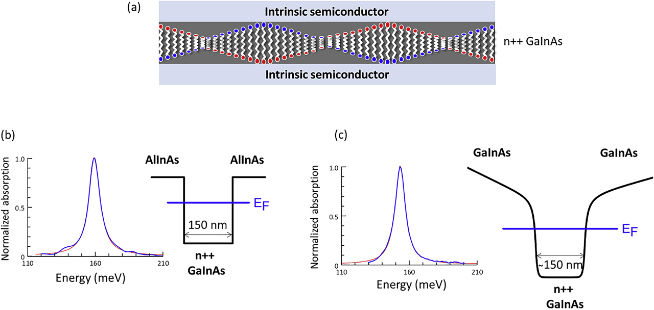
(a) Sketch of the system: a highly doped GaInAs layer embedded between two intrinsic semiconductor layers sustains a Berreman mode characterized by a dipole along the growth direction. (b) and (c) Conduction band profile and normalized absorption spectrum measured at 10° internal angle (blue line) for a sample in which the two intrinsic layers are (panel b) AlInAs barriers or (c) intrinsic GaInAs layers. Red lines are Lorentzian fit of the absorption spectra.
Plasmons appear in layers embedded between two confining barriers in a wide well configuration (Figure 1b). AlInAs barriers however are not necessary to confine a plasmon, as a simple heavily doped layer in an original “flat potential” bends the conduction band profile due to charge separation and form a potential well (Figure 1c). In both cases, the confining potential forms a set of discrete electronic energy levels which are the basis that we use for the theoretical description of these collective excitations. Given the wide dimension of the potential wells, 150 nm, it is remarkable that the electronic wavefunctions maintain their coherence and still form a set of energy states separated of few meV. The role of electronic confinement on plasmonic resonances with different potential geometries is therefore crucial to bring quantum engineering to the realm of plasmonics [22]. Moreover, a semiconductor platform instead of metals brings clear evidence on the quantum nature of the electrons building the plasmonic response. Figure 1b and c show measured normalized absorption spectra from two 150 nm doped layers that correspond to the potentials sketched in the figure. In both cases, the absorption has a Lorentzian shape and peaks at ∼160 meV, in excellent agreement with our theory reported in the study by Pegolotti et al [23]. Surprisingly, in spite of the disorder introduced by the donors, the spectra measured at small angles are characterized by sharp resonances with a quality factor on the order of 20. At higher angles, the collective excitations are dominated by spontaneous superradiant emission [13] and become radiatively broadened (Figure 2).
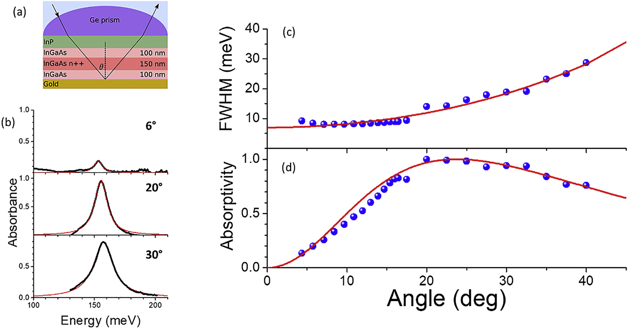
(a) Sketch of the sample and of the geometry used for reflectivity experiments. (b) Absorption spectra at three different internal angles (black lines) and Lorentzian fit of the resonances (red lines). (c) Full width at half the maximum (FWHM) of the absorption peak (blue symbols) as a function of the internal angle. Red line presents the calculated broadening, including radiative and nonradiative contribution. (d) Peak absorptivity extracted from the absorption spectra as a function of the angle, compared with the calculated one (red line) by using Eq. (3).
3 Superradiance, perfect absorption
The very strong interaction that plasmons have with light is intimately related to their collective nature, i.e., they are a symmetric superposition of all the optically active electronic transitions of the system. The optical properties of the plasmon mode have been calculated by solving quantum Langevin equations in the input–output formalism [24]. The bright plasmon is coupled with two bosonic baths: a bath of electronic excitations and a bath of free space photons. The coupling with the electronic bath is considered phenomenologically, and it gives rise to a nonradiative broadening γ of the plasmon mode, which is typically 20 times smaller than the plasmon frequency ΩP. The coupling between the plasmon and the free space photons is calculated thanks to our quantum model. It results in a radiative decay rate Γ, which is a function of the angle of emission, θ, and of the photon frequency ω through:
Γ0 depends on the oscillator strength of the plasmon, and its complete expression can be found in the study by Huppert et al [24]. It can be shown that Γ0 is proportional to the density of the electron gas, an indication of the superradiant nature of the plasmon emission [13]. The sin2 θ dependence in Eq. (2) comes from the fact that the plasmon has a dipole oriented along the growth direction, while the 1/cos θ dependence is associated with the photonic density of states. The angular dependence of the radiative rate allows us to vary the interaction between the plasmon and the electromagnetic field by simply changing the light propagation angle. As it will be discussed later, this permits to experimentally investigate different regimes of the light–matter interaction. It is also important to note that in our quantum model the spontaneous emission of the plasmons into the free space is calculated without employing a perturbative approach, and it results in a dependence of Γ on the photon frequency which is characteristics of non-Markovian dynamics.
The angular behavior of the plasmon spectra from the sample without the confining barriers (Figure 1c) has been experimentally investigated by performing reflectivity spectra, after evaporating a gold mirror on the surface. In order to span a wide angular range, we have illuminated the sample through a Germanium hemispherical lens, as sketched in Figure 2a. In this way, absorption spectra at internal angles between 6° and 40° have been measured. Few representative spectra are presented in Figure 2b, showing the Berreman mode and its evolution with the angle in terms of peak absorptivity and linewidth. In Figure 2c, the full width at half maximum of the absorption peaks, Γtot, is plotted as a function of the angle, θ. The results are well reproduced by Eq. (2) assuming that Γtot = γ + Γ(θ, ΩP) is the sum of the radiative and nonradiative contribution. By changing the propagation angle of the light, the radiative rate, Γ, varies from 0 to a value much bigger than the nonradiative rate, γ, as it can be seen in Figure 2c. At 6° internal angle, the radiative contribution to the plasmon linewidth is negligible, and therefore, we can extract the value of the nonradiative broadening, γ = 8 meV. The quality factor of the plasmon mode, centered at 153 meV, is thus 19. This value is quite remarkable as the plasmon is simply defined by the presence of a highly doped GaInAs region between two intrinsic GaInAs layers.
Figure 2d presents the peak absorptivity as a function of the internal angle extracted from the measured absorptivity spectra (symbols) and calculated (solid line) by using the result of our model which is expressed below, in Eq. (3). As expected from our quantum model, the peak absorptivity increases with increasing the angle up to θc = 20° where the critical coupling is reached. At this angle, the radiative loss rate equals nonradiative ones, which is the condition for perfect absorption where responsivity reaches 1. For greater angles, the peak absorptivity decreases while the linewidth increases. We also observe a blue shift of the plasmon peak, which can be well described as a cooperative Lamb shift [25]. Notice that the perfect absorption gives rise to a perfect blackbody emitter at the frequency of the Berreman mode.
The plasmon absorptivity is calculated by considering an optical input in our quantum model. In the presence of a single bright plasmon mode, close to a perfect gold mirror, the absorptivity is given by the following formula [24]:
This expression is obtained beyond the rotating wave approximation, and it takes into account the antiresonant terms of the light–matter interaction, responsible of the ultrastrong light–matter coupling [26]. Our model perfectly reproduces the experimental results, without using any fitting parameter, as it can be seen in Figure 2d. Three different regimes of the light–matter interaction can be identified. For small angles,
The absorption spectrum is thus Lorentzian, with a full width at half the maximum given by the nonradiative broadening. The amplitude of the peak is proportional to twice the radiative rate
The second regime occurs at the angle θc for which the radiative rate equals the nonradiative one:
This is the critical coupling regime, giving rise to perfect absorption at the plasmon frequency:
Our quantum model allows the description of incandescent emission induced by injecting an electrical current in the highly doped layer sustaining the Berreman mode [13], [27]. The application of an in-plane current induces the Joule heating of the electron gas and thus increases the temperature of the electronic reservoir Te with respect to that of the photonic one, Tph. In this out-of-equilibrium situation, the incandescent emission process can be seen as a plasmon-mediated exchange between the electronic and the photonic reservoir. The number of output photons, calculated by considering that both baths are in an incoherent thermal input state, is equal to the product of the absorptivity times the thermal occupancy at temperature Te [24]. This is equivalent to Kirchhoff’s law of thermal emission, stating the equivalence between the emissivity and the absorptivity at a given frequency and emission angle. The incandescent power
4 High frequency incandescent emission
Figure 3a presents a sketch of our device, which is fabricated exploiting a highly doped 45-nm GaInAs layer embedded between two undoped AlInAs barriers. This highly doped layer sustains a Berreman mode at 166 meV, which is inserted in a microcavity of total thickness 1.125 µm, delimited on the bottom by a highly doped 2-µm-thick GaInAs mirror. The sample has been grown by metal organic chemical vapor deposition and processed into a field-effect transistor-like structure, consisting of two ohmic contacts made of TiAu. The gate size is L × W = 50 × 50 µm2, where L and W stand for the length and width of the channel, respectively. On the top of the gate, we have realized a two-dimensional metallic grating by e-beam lithography and Au evaporation. The top part of Figure 3a presents a scanning electron microscope image of the grating, on which we have also indicated the dimensions of the square gold patches. The thickness of the cavity, defined as the distance between the bottom InGaAs mirror and the top grating, determines the energy of the cavity modes, while the ratio between the size of the patches and their periodicity determines the mode contrast, i.e., their coupling with free space. The right top part of Figure 3a presents the calculated absorption spectrum of the device. Due to the huge dipole of the collective electronic excitation, the cavity mode strongly couples with the Berreman mode and gives rise to polariton modes, as indicated in the spectrum. The grating parameters and the cavity thickness have been designed in order to have two polaritonic modes with peak absorptivity, and hence peak emissivity, close to 1. Figure 3b (top) shows the setup that has been used for our high frequency spectral resolved measurements. The plasmonic emitter is mounted on a high frequency holder to inject microwave into the electron gas that can also be biased with a direct current (dc) power supplier. The emitted power is collected into a Fourier transform infrared spectrometer and then measured using a fast Mercury Cadmium Telluride (MCT) detector with a frequency cutoff at 50 MHz. The spectra are measured in a step-scan mode using a high frequency lock-in amplifier. In the bottom part of Figure 3b, we indicate the temporal form of the input current used to modulate the temperature of the electron gas.
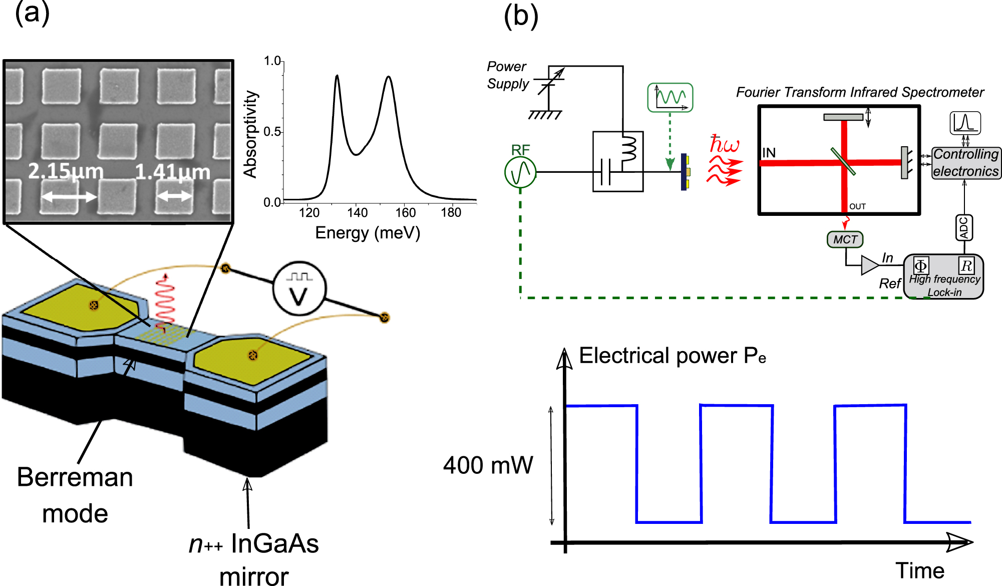
(a) Sketch of the device fabricated for thermal emission experiments. It consists of a 50 × 50 µm2 mesa with a top grating for the extraction of incandescent emission. In order to electrically excite the thermal emission, two lateral Ti/Au contacts (125 × 100 µm2) have been evaporated on the GaInAs layer sustaining the Berreman mode, after inductively coupled plasma reactive ion etching. The top part of the panel presents a scanning electron microscope image of the grating, with its characteristic dimensions, and the calculated absorption spectrum, displaying two polariton modes with almost unity peak absorptivity. (b) Sketch of the setup used for high frequency modulation of thermal emission. An electrical current is injected between the two lateral contacts. Its time modulation results in a modulation of the emitted power.
Experimental results of the frequency modulated thermal emission are shown in Figure 4a (dotted curve). In the insets of the figure, we provide spectra of the thermal emission for two frequency regimes. The spectra remain essentially identical, which proves that the emission signal arises from the incandescence of the polariton modes.
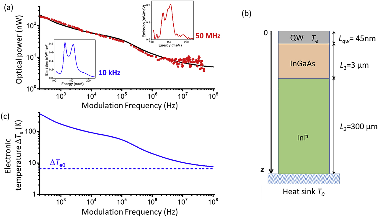
(a) Emitted power as a function of the modulation frequency (dots). The solid line is a result of modeling as described in the main text. The insets show two typical spectra for modulation frequency of 10 kHz and 50 MHz. (b) Schematic of semiconductor layers from the quantum well down to the heat sink used for our thermal model. (c) Estimations of the frequency-modulated part of the excess electronic temperature
In order to model the frequency dependence of the emitted power shown in Figure 4a, we developed a model that provides the temporal evolution of the electronic temperature Te. The model is one dimensional and assumes that the lattice temperature T(z) depends on a single spatial variable z (Figure 4b). The electronic temperature is different from the lattice temperature T(z) , and the thermal flux density that describes the heat exchanged between the electrons and the lattice is assumed to be of a simple form
Using energy conservation, we can write the following equations that couple the electronic and lattice temperature at the position of the quantum well z = 0:
with ce the thermal capacity of electrons, which can be assumed to be ce ≈ 103 J/m3 K at 300 K [28], Pe(t) the electrical power dissipated in the quantum well of thickness LQW and surface σ = 50 × 50 µm2, and λ1 = 5 W/m K the thermal conductivity of the InGaAs layer below the quantum well (Figure 4b). The lattice temperature T(t, z) satisfies the Fourier heat equation in each layer of the structure:
Here, Di is the thermal diffusion coefficient of the InGaAs and InP layers, with (i = 1) and (i = 2), respectively. The temperature and the thermal flux are continuous at the InGaAs/InP interface. The boundary condition at the heat sink is T(t, z = L1 + L2) = T0.
To analyze this problem, Pe (t) can be decomposed into Fourier series; then, it is sufficient to examine the temperature response to a thermal source that is of the form
Here,
Once the temperature
P0 is a constant adjusted so that the theoretical curve
All the physical parameters of the model are known except the constant β. The material parameters for InGaAs and InP are λ1 = 5 W/m K and D1 = 3.33 × 10⁻⁶ m2/s (the effect of the doping in the 2-µm-thick part has been neglected) and λ2 = 68 W/m K and D2 = 41 × 10−6 m2/s, respectively. The parameter β is determined from the best fit of the experimental data which provides β = 0.7 W/m K. As shown in Figure 4a, a very good fit of the optical power is obtained in the entire frequency range, which covers almost six decades. In Figure 4a, the bump observed at ∼105 Hz is due to the InGaAs/InP interface. Therefore, up to 1 MHz, the thermal dynamics of the system is dominated by the substrate underlying the electron gas. At higher frequencies, the curve flattens as only the electronic dynamics is sufficiently fast to provide a temperature change. Indeed, from the value of β = 0.7 W/m K, we determine the thermal cutoff frequency of the electron gas: ω0/(2π) = 55 GHz. Thermal sources based on electronic heating enable therefore an ultrafast modulation of thermal radiation. Notice that the value of the cutoff ω0 is determined fundamentally by the thermal coefficient β that sets the temperature difference between the electrons gas and the lattice. The reciprocal of the cutoff gives a time constant in the order of 18 ps, not far from the lifetime of the optical phonons (8 ps) which is, in our interpretation, the physical limit for the electron cooling at room temperature. Indeed, for shorter time than 1/ω0, the electron gas and the phonon bath are in thermal equilibrium via absorption and emission of optical phonons and have no temperature difference.
In Figure 4c, we plot the electronic temperature
5 Conclusions and perspectives
We have exploited the peculiar quantum properties of plasmons confined in semiconductor layers to demonstrate perfect absorption and dynamic modulation of thermal emission up to 50 MHz in the mid-infrared frequency range. When they are confined in a layer with thickness smaller than the plasma wavelength, confined plasmons are optically active and display absorption resonances, known as Berreman modes, with a quality factor in the order of 20 at low internal angle of light propagation. Plasmon radiative rate increases as a function of the angle of emission and largely exceeds the nonradiative rate, a demonstration of the superradiant character of this collective electronic excitation. We have demonstrated that when the radiative rate equals the nonradiative one, a critical coupling regime occurs, corresponding to perfect absorption of the plasmon mode. All our experimental results are supported by a quantum model of the plasmon optical properties, which goes beyond Markov and rotating wave approximation.
The optical properties of the plasmon have been exploited to realize a perfect blackbody, in which incandescence is induced by Joule heating of the electron gas. We have shown that a time modulation of the injected current results in a modulation of the incandescent emission, up to 50 MHz, limited by the detector bandwidth. Our experimental results have been analyzed through an analytical model which takes into account the different dynamic behavior of electronic and lattice temperature under Joule heating. This model gives an excellent agreement with the experimental results in the entire frequency range, which covers almost six decades.
Berreman modes in semiconductors offer a huge possibility to control emissivity, wavelength, directionality, and dynamic behavior of mid-infrared thermal sources in technologically mature material platforms. We believe that the versatility of this system can be beneficial to different fields of applications of thermal emitters, particularly whenever a high frequency response is necessary, like for thermal camouflage, friend-or-foe identification, or trace detection. Finally, the superradiant character of these excitations can be exploited also for radiative cooling in ultradense electronic circuits [30].
Funding source: Agence Nationale de la Recherche
Award Identifier / Grant number: ANR-14-CE26-0023-01
Acknowledgments
The authors acknowledge financial support from the Agence Nationale de la Recherche (Grant ANR-14-CE26-0023-01). The authors thank Stephan Suffit for help with the device fabrication, Eugenio Maggiolini for preliminary experiments on high modulation of thermal emission, Jean- Jacques Greffet for the loan of the 50 MHz-bandwidth MCT detector, and Emilie Sakat for discussions on the cavity design.
Author contribution: All the authors have accepted responsibility for the entire content of this submitted manuscript and approved submission.
Research funding: The authors acknowledge financial support from the Agence Nationale de la Recherche (Grant ANR-14-CE26-0023-01).
Conflict of interest statement: The authors declare no conflicts of interest regarding this article.
References
[1] R. A. Ferrell, “Predicted radiation of plasma oscillations in metal films,” Phys. Rev., vol. 111, pp. 1214–1222, 1958. https://doi.org/10.1103/physrev.111.1214.Search in Google Scholar
[2] A. R. Melnyk and M. J. Harrison, “Resonant excitation of plasmons in thin films by elecromagnetic waves,” Phys. Rev. Lett., vol. 21, pp. 85–88, 1968. https://doi.org/10.1103/physrevlett.21.85.Search in Google Scholar
[3] I. Lindau and P. O. Nilsson, “Experimental verification of optically excited longitudinal plasmons,” Phys. Scr., vol. 3, pp. 87–92, 1971. https://doi.org/10.1088/0031-8949/3/2/007.Search in Google Scholar
[4] A. R. Melnyk and M. J. Harrison, “Theory of optical excitation of plasmons in metals,” Phys. Rev. B, vol. 2, pp. 835–850, 1970. https://doi.org/10.1103/physrevb.2.835.Search in Google Scholar
[5] J. A. Scholl, A. L. Koh, and J. A. Dionne, “Quantum plasmon resonances of individual metallic nanoparticles,” Nature, vol. 483, pp. 421–427, 2012. https://doi.org/10.1038/nature10904.Search in Google Scholar
[6] W. P. Halperin, “Quantum size effects in metal particles,” Rev. Mod. Phys., vol. 58, pp. 533–606, 1986. https://doi.org/10.1103/revmodphys.58.533.Search in Google Scholar
[7] P. Mühlschlegel, H.-J. Eisler, O. J. F. Martin, B. Hecht, and D. W. Pohl, “Resonant optical antennas,” Science, vol. 308, p. 1607, 2005. https://doi.org/10.1126/science.1111886.Search in Google Scholar
[8] P. J. Schuck, D. P. Fromm, A. Sundaramurthy, G. S. Kino, and W. E. Moerner, “Improving the mismatch between light and nanoscale objects with gold bowtie nanoantennas,” Phys. Rev. Lett., vol. 94, p. 017402, 2005. https://doi.org/10.1103/physrevlett.94.017402.Search in Google Scholar
[9] M. S. Tame, K. R. McEnery, Ş. K. Özdemir, J. Lee, S. A. Maier, and M. S. Kim, “Quantum plasmonics,” Nat. Phys., vol. 9, pp. 329–340, 2013. https://doi.org/10.1038/nphys2615.Search in Google Scholar
[10] J. A. Mason, S. Smith, and D. Wasserman, “Strong absorption and selective thermal emission from a midinfrared metamaterial,” Appl. Phys. Lett., vol. 98, p. 241105, 2011. https://doi.org/10.1063/1.3600779.Search in Google Scholar
[11] S. Huppert, A. Vasanelli, T. Laurent, et al., “Radiatively broadened incandescent sources,” ACS Photonics, vol. 2, pp. 1663–1668, 2015. https://doi.org/10.1021/acsphotonics.5b00415.Search in Google Scholar
[12] S. Campione, F. Marquier, J. P. Hugonin, et al., “Directional and monochromatic thermal emitter from epsilon-near-zero conditions in semiconductor hyperbolic metamaterials,” Sci. Rep., vol. 6, p. 34746, 2016. https://doi.org/10.1038/srep34746.Search in Google Scholar
[13] T. Laurent, Y. Todorov, A. Vasanelli, et al., “Superradiant emission from a collective excitation in a semiconductor,” Phys. Rev. Lett., vol. 115, p. 187402, 2015. https://doi.org/10.1103/physrevlett.115.187402.Search in Google Scholar
[14] D. G. Baranov, Y. Xiao, I. A. Nechepurenko, A. Krasnok, A. Alù, and M. A. Kats, “Nanophotonic engineering of far-field thermal emitters,” Nat. Mater., vol. 18, pp. 920–930, 2019. https://doi.org/10.1038/s41563-019-0363-y.Search in Google Scholar
[15] J.-J. Greffet, R. Carminati, K. Joulain, J. P. Mulet, S. Mainguy, and Y. Chen, “Coherent emission of light by thermal sources,” Nature, vol. 416, pp. 61–64, 2002. https://doi.org/10.1038/416061a.Search in Google Scholar
[16] G. Lu, J. R. Nolen, T. G. Folland, M. J. Tadjer, D. G. Walker, & J. D. Caldwell, “Narrowband polaritonic thermal emitters driven by waste heat,” ACS Omega, vol. 5, pp. 10900–10908, 2020. https://doi.org/10.1021/acsomega.0c00600.Search in Google Scholar
[17] T. Wang, P. Li, D. N. Chigrin, et al., “Phonon-polaritonic bowtie nanoantennas: controlling infrared thermal radiation at the nanoscale,” ACS Photonics, vol. 4, pp. 1753–1760, 2017. https://doi.org/10.1021/acsphotonics.7b00321.Search in Google Scholar
[18] M. De Zoysa, T. Asano, K. Mochizuki, A. Oskooi, T. Inoue, & S. Noda, “Conversion of broadband to narrowband thermal emission through energy recycling,” Nat. Photonics, vol. 6, pp. 535–539, 2012. https://doi.org/10.1038/nphoton.2012.146.Search in Google Scholar
[19] Z.-Y. Yang, S. Ishii, T. Yokoyama, et al., “Narrowband wavelength selective thermal emitters by confined tamm plasmon polaritons,” ACS Photonics, vol. 4, pp. 2212–2219, 2017. https://doi.org/10.1021/acsphotonics.7b00408.Search in Google Scholar
[20] T. Inoue, M. D. Zoysa, T. Asano, and S. Noda, “Realization of dynamic thermal emission control,” Nat. Mater., vol. 13, pp. 928–931, 2014. https://doi.org/10.1038/nmat4043.Search in Google Scholar
[21] B. Askenazi, A. Vasanelli, A. Delteil, et al., “Ultra-strong light–matter coupling for designer Reststrahlen band,” New J. Phys., vol. 16, p. 043029, 2014. https://doi.org/10.1088/1367-2630/16/4/043029.Search in Google Scholar
[22] A. Vasanelli, S. Huppert, A. Haky, T. Laurent, Y. Todorov, and C. Sirtori, Semiconductor quantum plasmonics, Available at: https://arxiv.org/abs/2003.01543v2.Search in Google Scholar
[23] G. Pegolotti, A. Vasanelli, Y. Todorov, and C. Sirtori, “Quantum model of coupled intersubband plasmons,” Phys. Rev. B, vol. 90, p. 035305, 2014. https://doi.org/10.1103/physrevb.90.035305.Search in Google Scholar
[24] S. Huppert, A. Vasanelli, G. Pegolotti, Y. Todorov, and C. Sirtori, “Strong and ultrastrong coupling with free-space radiation,” Phys. Rev. B, vol. 94, p. 155418, 2016. https://doi.org/10.1103/physrevb.94.155418.Search in Google Scholar
[25] G. Frucci, S. Huppert, A. Vasanelli, et al., “Cooperative Lamb shift and superradiance in an optoelectronic device,” New J. Phys., vol. 19, p. 043006, 2017. https://doi.org/10.1088/1367-2630/aa631d.Search in Google Scholar
[26] C. Ciuti, G. Bastard, and I. Carusotto, “Quantum vacuum properties of the intersubband cavity polariton field,” Phys. Rev. B, vol. 72, p. 115303, 2005. https://doi.org/10.1103/physrevb.72.115303.Search in Google Scholar
[27] T. Laurent, Y. Todorov, A. Vasanelli, I. Sagnes, G. Beaudoin, & C. Sirtori, “Electrical excitation of superradiant intersubband plasmons,” Appl. Phys. Lett., vol. 107, p. 241112, 2015. https://doi.org/10.1063/1.4937806.Search in Google Scholar
[28] A. N. Chakravarti, K. P. Ghatak, S. Ghosh, and A. K. Chowdhury, “Effect of heavy doping on the electronic heat capacity in semiconductors,” Phys. Status Solidi (b), vol. 109, pp. 705–710, 1982. https://doi.org/10.1002/pssb.2221090229.Search in Google Scholar
[29] V. Spagnolo, G. Scamarcio, H. Page, and C. Sirtori, “Simultaneous measurement of the electronic and lattice temperatures in GaAs/Al0.45Ga0.55As quantum-cascade lasers: influence on the optical performance,” Appl. Phys. Lett., vol. 84, pp. 3690–3692, 2004. https://doi.org/10.1063/1.1739518.Search in Google Scholar
[30] S. Buddhiraju, W. Li, and S. Fan, “Photonic refrigeration from time-modulated thermal emission,” Phys. Rev. Lett., vol. 124, p. 077402, 2020. https://doi.org/10.1103/physrevlett.124.077402.Search in Google Scholar
© 2020 Angela Vasanelli et al., published by De Gruyter, Berlin/Boston
This work is licensed under the Creative Commons Attribution 4.0 International License.
Articles in the same Issue
- Editorial
- Editorial
- Optoelectronics and Integrated Photonics
- Disorder effects in nitride semiconductors: impact on fundamental and device properties
- Ultralow threshold blue quantum dot lasers: what’s the true recipe for success?
- Waiting for Act 2: what lies beyond organic light-emitting diode (OLED) displays for organic electronics?
- Waveguide combiners for mixed reality headsets: a nanophotonics design perspective
- On-chip broadband nonreciprocal light storage
- High-Q nanophotonics: sculpting wavefronts with slow light
- Thermoelectric graphene photodetectors with sub-nanosecond response times at terahertz frequencies
- High-performance integrated graphene electro-optic modulator at cryogenic temperature
- Asymmetric photoelectric effect: Auger-assisted hot hole photocurrents in transition metal dichalcogenides
- Seeing the light in energy use
- Lasers, Active optical devices and Spectroscopy
- A high-repetition rate attosecond light source for time-resolved coincidence spectroscopy
- Fast laser speckle suppression with an intracavity diffuser
- Active optics with silk
- Nanolaser arrays: toward application-driven dense integration
- Two-dimensional spectroscopy on a THz quantum cascade structure
- Homogeneous quantum cascade lasers operating as terahertz frequency combs over their entire operational regime
- Toward new frontiers for terahertz quantum cascade laser frequency combs
- Soliton dynamics of ring quantum cascade lasers with injected signal
- Fiber Optics and Optical Communications
- Propagation stability in optical fibers: role of path memory and angular momentum
- Perspective on using multiple orbital-angular-momentum beams for enhanced capacity in free-space optical communication links
- Biomedical Photonics
- A fiber optic–nanophotonic approach to the detection of antibodies and viral particles of COVID-19
- Plasmonic control of drug release efficiency in agarose gel loaded with gold nanoparticle assemblies
- Metasurfaces for biomedical applications: imaging and sensing from a nanophotonics perspective
- Hyperbolic dispersion metasurfaces for molecular biosensing
- Fundamentals of Optics
- A Tutorial on the Classical Theories of Electromagnetic Scattering and Diffraction
- Reflectionless excitation of arbitrary photonic structures: a general theory
- Optimization Methods
- Multiobjective and categorical global optimization of photonic structures based on ResNet generative neural networks
- Machine learning–assisted global optimization of photonic devices
- Artificial neural networks for inverse design of resonant nanophotonic components with oscillatory loss landscapes
- Adjoint-optimized nanoscale light extractor for nitrogen-vacancy centers in diamond
- Topological Photonics
- Non-Hermitian and topological photonics: optics at an exceptional point
- Topological photonics: Where do we go from here?
- Topological nanophotonics for photoluminescence control
- Anomalous Anderson localization behavior in gain-loss balanced non-Hermitian systems
- Quantum computing, Quantum Optics, and QED
- Quantum computing and simulation
- NIST-certified secure key generation via deep learning of physical unclonable functions in silica aerogels
- Thomas–Reiche–Kuhn (TRK) sum rule for interacting photons
- Macroscopic QED for quantum nanophotonics: emitter-centered modes as a minimal basis for multiemitter problems
- Generation and dynamics of entangled fermion–photon–phonon states in nanocavities
- Polaritonic Tamm states induced by cavity photons
- Recent progress in engineering the Casimir effect – applications to nanophotonics, nanomechanics, and chemistry
- Enhancement of rotational vacuum friction by surface photon tunneling
- Plasmonics and Polaritonics
- Shrinking the surface plasmon
- Polariton panorama
- Scattering of a single plasmon polariton by multiple atoms for in-plane control of light
- A metasurface-based diamond frequency converter using plasmonic nanogap resonators
- Selective excitation of individual nanoantennas by pure spectral phase control in the ultrafast coherent regime
- Semiconductor quantum plasmons for high frequency thermal emission
- Origin of dispersive line shapes in plasmon-enhanced stimulated Raman scattering microscopy
- Epitaxial aluminum plasmonics covering full visible spectrum
- Metaoptics
- Metamaterials with high degrees of freedom: space, time, and more
- The road to atomically thin metasurface optics
- Active nonlocal metasurfaces
- Giant midinfrared nonlinearity based on multiple quantum well polaritonic metasurfaces
- Near-field plates and the near zone of metasurfaces
- High-efficiency metadevices for bifunctional generations of vectorial optical fields
- Printing polarization and phase at the optical diffraction limit: near- and far-field optical encryption
- Optical response of jammed rectangular nanostructures
- Dynamic phase-change metafilm absorber for strong designer modulation of visible light
- Arbitrary polarization conversion for pure vortex generation with a single metasurface
- Enhanced harmonic generation in gases using an all-dielectric metasurface
- Monolithic metasurface spatial differentiator enabled by asymmetric photonic spin-orbit interactions