Disorder effects in nitride semiconductors: impact on fundamental and device properties
-
Claude Weisbuch
 ,
Shuji Nakamura
,
Shuji Nakamura

Abstract
Semiconductor structures used for fundamental or device applications most often incorporate alloy materials. In “usual” or “common” III–V alloys, based on the InGaAsP or InGaAlAs material systems, the effects of compositional disorder on the electronic properties can be treated in a perturbative approach. This is not the case in the more recent nitride-based GaInAlN alloys, where the potential changes associated with the various atoms induce strong localization effects, which cannot be described perturbatively. Since the early studies of these materials and devices, disorder effects have indeed been identified to play a major role in their properties. Although many studies have been performed on the structural characterization of materials, on intrinsic electronic localization properties, and on the impact of disorder on device operation, there are still many open questions on all these topics. Taking disorder into account also leads to unmanageable problems in simulations. As a prerequisite to address material and device simulations, a critical examination of experiments must be considered to ensure that one measures intrinsic parameters as these materials are difficult to grow with low defect densities. A specific property of nitride semiconductors that can obscure intrinsic properties is the strong spontaneous and piezoelectric fields. We outline in this review the remaining challenges faced when attempting to fully describe nitride-based material systems, taking the examples of LEDs. The objectives of a better understanding of disorder phenomena are to explain the hidden phenomena often forcing one to use ad hoc parameters, or additional poorly defined concepts, to make simulations agree with experiments. Finally, we describe a novel simulation tool based on a mathematical breakthrough to solve the Schrödinger equation in disordered potentials that facilitates 3D simulations that include alloy disorder.
1 Introduction
Modern semiconductor structures and devices combine different elements, compounds and alloys to form heterostructures. Their importance was recognized by the attribution of the 2000 physics Nobel prize to Zhores Alferov and Herbert Krömer who developed the concepts that resulted in the field of bandgap engineering. To realize many heterostructure designs, the material palette includes alloys because pure compounds or elements often do not have the necessary material properties for specific heterostructure designs. This is best seen in Figure 1, which shows the bandgap map of the major semiconductors. With the exception of the GaAs/AlAs material pair, where the compound materials are nearly lattice matched, other pure compound pairs typically have large lattice mismatched. To obtain materials with acceptable defect levels, strain is reduced compared with pure compound associations by using alloys with intermediate lattice constants in heterostructures. Alloys have random substitutions of atoms at well-defined sites within the crystal structure (these alloys do not have positional disorder). Therefore, electrons and holes experience a random potential at a scale of the unit cell.
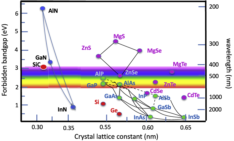
Bandgap map of major semiconductors.
In usual III–Vs, alloy disorder has nonessential consequences. As the disorder-induced potential fluctuations are weak, band structure properties can be described by the virtual crystal approximation (VCA) where each potentially disordered atom site is substituted by an artificial atom interpolating between the properties of the actual constituent atoms (we leave outside this review the very different case of disordered semiconductors where disorder is introduced through dopants, see the study by Shklovskii and Efros [1] for a very thorough analysis). Thus, the crystal is perfectly ordered and carrier quantum states are Bloch waves. To account for disorder, a perturbation is introduced, which is the potential difference between the VCA atom potential and the real atom potential. This allows computation, for example, of the alloy disorder contribution to mobility, as well as the bowing parameter determining the quadratic variation of the bandgap with alloy composition.
In contrast, the random potential due to alloy disorder in nitride semiconductors is so large that it leads to localization properties that cannot be described as perturbations. This significantly impacts in a major way many fundamental properties of the group III nitrides. However, so far, no full microscopic model exists yet to describe optical and transport phenomena as four challenges exist: (1) modeling requires accurate microscopic descriptions of alloy heterostructures, with some open questions on alloy randomness, interface abruptness and composition variation along the growth direction; (2) the high extended and point defect densities existing in nitride materials can add another level of complexity for the description of the physical system. For instance, the large difference between optoelectronic performance of molecular beam epitaxy (MBE)-grown materials compared with metal-organic chemical vapor deposition (MOCVD)-grown ones is still mysterious, although part of the explanation could be due to the presence of Ca impurities in MBE material acting as a killer impurity [2]; another such major effect is the curing of some nonradiative (NR) recombination centers by the growth of superlattices or underlayers before growing the active LED layers [3], recently attributed to the trapping by these structures of surface defects in GaN [4]; in MOCVD materials grown under optimal conditions, NR defects appear in selected layers such as AlGaN electron–blocking layers (EBLs) or in higher In content layers for green LEDs [5], [6], [7], [8]; (3) for the electronic quantum description, a number of phenomena need to be further explored such as electron-hole carrier localization and tunneling, Coulomb interactions, … Simulations of basic optical properties requires the computation of numerous energy levels, energy relaxation toward emitting levels, computation of the carrier population, … Simulations of LEDs require the additional computation of transport coefficients taking disorder and localization into account, both for perpendicular transport (I–V characteristics of LEDs, unipolar barrier transport) and in-plane transport. All these tasks require huge computational resources; (iv) finally, for comparisons with simulations, experiments need to determine accurate parameters, avoiding systematic errors.
We discuss disorder effects in nitride alloys in the context of LEDs, as most of these challenges occur there, and their many studies result in a lot of data, as well as in improved materials and devices. In addition, there are fewer carrier transport studies being conducted as alloys are avoided in transistors as their uses in the active channel lead to much reduced mobilities [9]. We emphasize in this article the large number of prerequisites required for a full understanding of LED materials and devices such as the need for intrinsic material parameters, carefully executed experiments and interpretation and powerful computational tools. We also mention alloy-based energy barriers, as they have very weak rectifying properties while they play major roles in devices and need serious design efforts to reach their expected barrier role [10], [11], [12].
2 Why do we need to consider disorder effects in nitride LEDs?
There is ample evidence of alloy-induced disorder effects on material and device properties, which can be classified as directly observable either at a microscopic scale or at macroscopic scale through spatially averaged effects of disorder or indirectly observable where the measured effects are different from those modeled without taking disorder into account. Understanding and modeling the effects of disorder is required if one wishes to reach the physical limits of efficiency in LEDs. At stake is the huge improvement in energy savings still permitted by the physics of nitride LEDs: present day maximum efficiency is ∼200 lm/W for white-emitting phosphor-converted LEDs, whereas color mixed LEDs, so far less efficient because of the green gap, could reach 330 lm/W when the full potential of LEDs is reached [13].
3 Experimental evidence of directly observable disorder-induced effects
Optical spectroscopy at the nanoscale should allow direct measurements of alloy disorder-induced energy and localization effects (Figure 2b). There are many observations of compositional variations at the few 100-nm micron length scale through microphotoluminescence [15], near-field scanning optical microscope [16], spatially-resolved cathodoluminescence [17], with a spatial resolution down to ∼50 nm. These techniques are used to measure fluctuations that are either intrinsic to alloy disorder or due to details in growth such as QW thickness fluctuations or more involved fluctuations due to specific details of the growth surface [18]. As the scale of intrinsic disorder of alloys is a few nm (Figure 2b), it is not observed through these techniques. Only the recently developed technique of scanning tunneling luminescence (STL) provides spatial resolution at the few-nm scale and allows direct observation of localized states induced by the intrinsic disorder [19].
![Figure 2: (a) Schematics of the blue-emitting LED to be modeled with 3-nm thick Ino.14Ga0.86N quantum wells (QWs) and 7-nm thick GaN barriers; (b) in-plane disordered electron and hole effective energy levels computed with the localization landscape (LL) theory (see below). The emission energy observed at the nanoscale of disorder should reveal the local disordered-localization energy; (c) in-plane averaged, computed band extrema along the growth direction under 2.8 V forward bias. Black curves show the averaged band extrema obtained from the compositional map, whereas the red and green curves show the averaged band extrema computed through the LL theory. The inset shows the effect of quantum disorder, raising and lowering energy extrema due to in-plane quantum confinement and tunneling (from [14]).](/document/doi/10.1515/nanoph-2020-0590/asset/graphic/j_nanoph-2020-0590_fig_002.jpg)
(a) Schematics of the blue-emitting LED to be modeled with 3-nm thick Ino.14Ga0.86N quantum wells (QWs) and 7-nm thick GaN barriers; (b) in-plane disordered electron and hole effective energy levels computed with the localization landscape (LL) theory (see below). The emission energy observed at the nanoscale of disorder should reveal the local disordered-localization energy; (c) in-plane averaged, computed band extrema along the growth direction under 2.8 V forward bias. Black curves show the averaged band extrema obtained from the compositional map, whereas the red and green curves show the averaged band extrema computed through the LL theory. The inset shows the effect of quantum disorder, raising and lowering energy extrema due to in-plane quantum confinement and tunneling (from [14]).
The indirect impact of nm-scale disorder can however be observed at the macroscopic level, through spatially averaged observations. For instance, the increase in emission linewidth compared with pure compounds reflects the variations in local composition, as does the absorption edge broadening [20].
Another macroscopically observed effect of nanoscale disorder is the Stokes shift, that is, the difference between emission and absorption energies. We note that the Stokes shift was originally invoked in the context of molecular fluorescence with well-defined peak emission energies and absorption energies. In semiconductors, both phenomena are broadened by disorder. Thus, taking the Stokes shift as a quantitative measurement of disorder is uncertain, at best, as both emission and absorption edges are poorly defined: namely, in QWs, from which most data originate, the absorption edge and emission peak are broadened and shifted by the quantum-confined Stark effect (QCSE) in nitrides because of the electron-hole separation induced by the internal electric fields. Sorting the smaller contribution of disorder is challenging. One could use opposite dopants on both QWs’ sides to completely screen the polarization field induced by the spontaneous polarization difference at the InGaN/GaN interface [21]. To avoid the QCSE in QWs altogether and measure intrinsic absorption and emission of InGaN alloys, one should use thick InGaN layers such that the effects of the QCSE can be avoided [22]. In both cases of thin and thick materials, the absorption curve is often approximated by a sigmoid function [23], which for QWs includes both the effect of disorder and the QCSE (Figure 3a). As for emission energy, it is difficult to assign it an accurate value because the emission peak results from the history of carrier energy relaxation, and the high-energy emission edge is even more dependent on experimental conditions (temperature, carrier density). Therefore, the very large Stokes shifts, up to several hundreds of meV [23], [24], reported might mainly be due to a large QCSE in the case of QWs and large inhomogeneities of materials as a result of poorly controlled growth (see, e.g., the small Stokes shift of bulk material in Figure 3a compared with the study by O’Donnell et al. [25]). The dominant impact of the QCSE on the Stokes shift in multiple quantum wells (MQWs) is measured in MQW structures with constant In concentration and variable thickness (Figure 3a) [26], [27] (for recent measurements on industry-grade materials, see also the study by Nippert [28], p. 32). Applying bias allows to cancel the QCSE when reaching flat-band conditions [31], [32] but should also measure emission under such conditions to extract a value for Stokes shift void of QCSE. In any case, instead of the sigmoid function, one could use the Tauc plot of the band edge absorption, used in many other disordered systems [33] where the bandgap is defined as the intercept of the extrapolated to zero absorption of the quantity (αhν)2, where α is the absorption coefficient of the material, with the photon energy hν as the abscissa (Figure 3c). The best identification of band edge states in absorption is revealed on a log scale as the Urbach tail of absorption [34], but this is not what is analyzed in the articles stating large Stokes shifts.
![Figure 3: (a) Photoluminescence (PL) and PL excitation (PLE) spectra of InGaN bulk (80-nm thick) and QW (3- and 6.2-nm thick) materials. The bulk material exhibits a small Stokes shift, characteristic of alloy disorder. A large Stoke shift is observed for QWs. Approximating the absorption curve by a sigmoid and the absorption edge Eabs as its center leads to a large Stokes shift dependent on the QW thickness (after the study by Berkowicz et al. [26]); (b) example of the S-shape temperature dependence of the peak energy for InGaN-related PL (after the study by Cho et al. [29]); (c) example of a Tauc plot of a ZnO thin film fitting the linear region to evaluate the bandgap at the x-axis intercept (after the study by Yang et al. [30]).](/document/doi/10.1515/nanoph-2020-0590/asset/graphic/j_nanoph-2020-0590_fig_003.jpg)
(a) Photoluminescence (PL) and PL excitation (PLE) spectra of InGaN bulk (80-nm thick) and QW (3- and 6.2-nm thick) materials. The bulk material exhibits a small Stokes shift, characteristic of alloy disorder. A large Stoke shift is observed for QWs. Approximating the absorption curve by a sigmoid and the absorption edge Eabs as its center leads to a large Stokes shift dependent on the QW thickness (after the study by Berkowicz et al. [26]); (b) example of the S-shape temperature dependence of the peak energy for InGaN-related PL (after the study by Cho et al. [29]); (c) example of a Tauc plot of a ZnO thin film fitting the linear region to evaluate the bandgap at the x-axis intercept (after the study by Yang et al. [30]).
A more indirect probe of disorder is provided by the so-called S-shaped curve displayed by the change of the peak emission wavelength with temperature (Figure 3b): starting at a low temperature (and increasing the temperature), the decrease in peak energy from 10 to 70 K is interpreted due to improved thermalization between localized states, reaching deeper states, followed at higher temperatures, 70–150 K, by escape from deep localized states into delocalized states emitting at higher energies. At still higher temperatures, the emission energy decreases with the temperature along the materials’ bandgap. Another probe of disorder is the blue shift in emission energy with increased carrier injection due to band filling of disorder-broadened states, although the major part of the shift in c-plane materials is due to internal field screening of the QCSE in QWs. Other optical evidence of disorder-induced localization is provided by indirect effects such as increased Auger recombination coefficient (discussed in the following sections) or longitudinal-optical (LO) phonon replicas of emission [35] (see, e.g., the lower emission spectrum in Figure 3a).
4 Experimental evidence of indirectly observed disorder-induced effects
Indirectly observed disorder effects are inferred when the modeling of materials and device characteristics cannot describe the measured effects without accounting for disorder.
In-plane carrier transport properties are of course sensitive to the in-plane potential fluctuations such as those in Figure 2b as revealed by electron mobilities [9] or carrier diffusion lengths [36], [37], [38]. The most direct evaluation of electron localization properties should be the electrical measurements of carrier mobilities. However, the impact of these electrons and hole localization has not yet been theoretically assessed on the in-plane carrier transport properties. The electron mobility measurements of Sohi et al. [9] could be explained by a simple perturbative model for electron mobility in InGaN HEMT channels at high carrier densities (2.47 × 1013 cm−2) at room temperature, conditions under which one expects diminished effects of disorder. The mobility decreases from 1340 to 173 cm2 V−1 s−1 when the In content varies from 0 to 20%. A surprisingly good agreement with theory is realized by crudely taking an alloy fluctuation potential equal to the conduction band offset between InN and GaN. It remains to be seen whether strong localization would be observed at low temperatures and reduced electron densities.
Vertical transport properties of multilayer LED bipolar structures are also strongly impacted by disorder, but there, disorder improves the transport properties! One would expect that the LED forward voltage VF (defined as the voltage for a sizeable current, usually 20 or 35 20 A/cm−2) as displayed in I–V characteristic curves is such that the energy supplied per electron–hole (e–h) pair by the energy source, eV, is equal to the photon energy. This is indeed observed experimentally, at least in blue single QW LEDs, and in usual III–V LEDs. This is due to the electron and hole (e–h) quasi-Fermi levels being near the respective e–h QW levels, therefore significantly populating them, which leads to a sizeable recombination current. However, for nitride MQW LEDs, where quantum barriers and internal fields hinder well-to-well carrier transport, experiments show excess voltages for longer wavelength LEDs with high indium content in the InGaN QWs. On the theory side, 1D simulations always show larger VF than experimentally observed, the more so for long-wavelength LEDs. These 1D simulation tools, which obviously cannot include in-plane disorder, need an ad hoc artificial correction of the internal fields to reach reasonable onset values. Although some of the excess voltage can be attributed to large band discontinuities and increased polarization-induced barriers (due to discontinuities of the spontaneous and strain-induced polarization), 1D simulations miss two effects of disorder: first, the in-plane averaged effective barrier height is reduced by compositional fluctuations (Figure 1c); second, percolative carrier transport paths in the disordered potential greatly reduce the effective barrier height carriers (see Figure 8d). The same percolative transport phenomenon is at work in explaining why unipolar energy barriers always display a much reduced resistance to current and even are often ohmic without the rectifying behavior [10], [11], [12].
Another often invoked indirect impact of disorder is the high radiative efficiency for blue-violet LEDs [39], [40], seen as a surprise, given that the threading dislocation density is on the order of 108–109 cm−2 when grown on sapphire, values prohibiting efficient recombination in other III–V semiconductors [41]. Some have invoked a lower activity of dislocations in nitrides [42], [43], [44], [45], [46]. However, at the beginning of high-efficiency blue LEDs, the preferred explanation was that disorder-induced localization would prevent carriers to reach NR recombination centers [47]. Indeed, the diffusion lengths in active layers, most often alloy QWs, are quite small compared with other materials (although measured values vary substantially [38], [48]), which can make the capture radius of carriers by dislocations smaller than the dislocation separation. The situation is complex to analyze as carriers appear to be thermalized between localized and delocalized states as revealed by the thermal tails of emission in operating LEDs, which indicates a limited effect of localization.
5 The efficiency loss, “droop”, at high current densities in nitride LEDs—the role of disorder
A major issue in nitride LED efficiency, at blue and other wavelengths, is the internal quantum efficiency (IQE) droop under high driving current densities. Although peak IQEs reach the 90+% range for blue-violet LEDs, these values are achieved at current densities of a few A/cm2.
The droop phenomenon is less prevalent in other III–V materials systems as these operate at much lower carrier densities. This originates from the strong QCSE in nitride QWs, which leads to comparatively small radiative recombination coefficient, thus requiring larger carrier densities to emit a given photon flux [31]. Therefore, nonlinear NR effects such as the Auger recombination become more important than in the conventional III–Vs.
The droop phenomenon is often analyzed through the so-called ABC model of the IQE, where A is the Shockley–Read–Hall NR recombination coefficient, B is the bimolecular radiative recombination coefficient and the Cn3 term is a nonlinear NR recombination term. In this ABC model of droop, the injected current density in the LED J and IQE are given by the following:
where e is the electron charge, d is the active layer thickness, n is the electron concentration (equal to the hole density p in the nominally undoped active layers), IE is the injection efficiency (fraction of injected e–h pairs that are captured in the active QWs). These two equations are “reasonably” verified in LEDs [49], [50], but with a very wide range of parameters that all lead to excellent fits (Figure 4) (see, e.g., the study by Weisbuch et al. [51] for a discussion of the extraction of the ABC parameters from the external quantum efficiency (EQE) curve analysis). In addition, the ABC analysis, although very attractive due to its simplicity, depends on a number of important critical approximations: (1) A, B and C are not independent of carrier density. In c-plane–grown nitrides, the internal spontaneous and piezoelectric-related electric fields are progressively screened with increasing injected carrier density, changing accordingly A, B and C; (2) carrier localization effects, such as due to In compositional fluctuations, also change with n; (3) carrier injection is not uniform in the various QWs of MQW LEDs (in particular holes), leading to an inhomogeneous distribution of carriers among QWs, hence of recombination rates between QWs; thus, each QW has its own A, B and C coefficients due to their dependences on carrier densities; (4) density-dependent current crowding at contacts can lead to lateral inhomogeneous carrier distribution, thus A, B and C depend on the position on the chip [52]. For an experimental analysis of variables A, B and C with carrier injection and composition, see the studies by David et al. and David and Hurni [49], [50].
![Figure 4: (a) Example of ABC fit of EQE vs. injected current in an eight-QW LED. The IQE is 76% as calculated from the position of the peak EQE; (b) calculated C coefficient as a function of B, considering that one or all eight QWs are populated, fitting the IQE curve on the left. Data points correspond to different values of B reported in the literature. Reproduced from the study by Weisbuch et al. [51]; see details there.](/document/doi/10.1515/nanoph-2020-0590/asset/graphic/j_nanoph-2020-0590_fig_004.jpg)
(a) Example of ABC fit of EQE vs. injected current in an eight-QW LED. The IQE is 76% as calculated from the position of the peak EQE; (b) calculated C coefficient as a function of B, considering that one or all eight QWs are populated, fitting the IQE curve on the left. Data points correspond to different values of B reported in the literature. Reproduced from the study by Weisbuch et al. [51]; see details there.
There has been long arguing about the physical mechanism at the origin of the Cn3 term. At first, the cause for droop was thought to be of extrinsic nature because of decreasing IE [53] or carrier delocalization from localized states with high IQE at increased currents [47]. This changed dramatically when Shen et al. [54] announced that droop was due to an intrinsic effect, the Auger effect, through an analysis by the ABC modeling, using carrier lifetime changes with carrier density. This started many efforts to unambiguously determine the origin of droop because the measured Auger coefficient, 1.4–2.0 × 10⁻³⁰ cm6 s−1 [54], was orders of magnitude larger than direct three-body calculations in bulk materials [55]. Then, theorists calculated the effects of indirect phonon-assisted mechanisms or of QW finite thickness [56], [57], [58], [59], however, still with smaller values than measured ones, which led to continuing disputing the Auger mechanism with others mechanisms such as diminished IE due to carrier escape [53] or overshoot [60] from active regions (see Figure 6). However, the evidence for carriers escaping the active region relied on misleading interpretations of measurements: forward minority electron current in the LED top p-layer can be mistaken for escape current, whereas it is due to Auger electrons bypassing the EBL [61], [62], [63] (it is remarkable that although Vampola et al. [61] concluded that both thermal escape and Auger-assisted electron overflow of electrons could explain his data, most authors citing this article use it as proof of thermal escape of electrons); reverse photocurrent under low bias has been mistaken as an NR recombination channel (for a full discussion of issues in optical measurements, see the study by David et al. [49]).
Then, experimentally, the signature of Auger-generated hot electrons by electron emission in vacuum provided direct proof of the Auger mechanism [64], and theoretically, it became clear compositional fluctuations would increase the apparent Auger recombination coefficient C [65] (see the following sections).
The connection between disorder and the Auger droop is experimentally well confirmed by the smaller droop or its absence in PL measurements of GaN QWs free from alloy disorder [66], [67].
6 A prerequisite to simulations: the microscopic description of the simulated structures
The material system to be modeled requires the accurate knowledge of both their geometry and composition. These are often limiting factors of simulations due to uncertainty in either structure or physical parameters.
For instance, it is well-known that the transport and optical properties of heterostructures are very sensitive to their detailed geometry. Already in GaAs QWs, interface roughness shows up as a major source of intrinsic geometric disorder leading to inhomogeneous broadening in optical spectroscopy [68]. In turn, interface disorder impacts the design of short wavelength GaAs/AlGaAs lasers [69] and also leads to localization properties at a low temperature displayed by a mobility edge [70]. In the nitride materials system, the fact that the QW material is an alloy leads to a much more complex situation. First, the randomness of the alloy has to be assessed: indium clustering leading to In compositional fluctuations larger than those expected from exact alloy randomness was first invoked to explain the high efficiency of LEDs [25], [71]. Although clustering, indeed observed by transmission electron microscopy (TEM), was later proven as due to TEM measurement artifacts (clustering was created under strong electron irradiation [72]), a recent article suggests the existence of short range clustering, not to be detected in atomic probe tomography (APT) due to the limited detection efficiency of most APT systems [73]. This claim appears however controversial as randomness evaluations in high-efficiency APT systems still conclude to perfect randomness. Second, the geometrical definition of interfaces for QWs, leading, or not, to interface roughness is hard to assess in III nitrides. The composition varies progressively in the growth direction, with the lower interface being abrupt and the upper interface somewhat diffuse, with some In being also present in barriers because of memory effects of growth systems. Attributing interface roughness geometries at nm scale under such conditions is difficult, but evaluations through APT and TEM conclude to interface fluctuations ∼5 nm wide and 1–2 monolayer thick [74], [75]. These modified interface geometries help improve simulations of luminescence spectra [76] and of the Urbach tail of the absorption edge [34]. Such measurements are spatially averaged effects of interface disorder and one would wish more direct observations of the interface fluctuations. The STL technique provides spatial resolution at the few nm scale and could probe the interface morphology because of the very localized nature of the probing carrier density [19].
7 Which quantities are to be modeled?—issues in their measurements
For optical properties of LEDs, one needs to simulate the dependence of the emission wavelength on In content, QW thickness and applied bias. The quantities entering equations (1) and (2), namely the A, B and C coefficients and the IE, although their determination require great care as discussed previously, are needed to obtain the IQE. IE is a particularly difficult quantity to measure, and we refer to the detailed discussion in the study by Weisbuch [77]. In addition, great care must be exerted when extracting coefficients from purely optical excitation measurements for use in LED simulations as the internal fields are different from those under electrical excitation. For a description of best practices for such measurements, see the study by David et al. [49].
It is easier to measure the I–V characteristic of an LED, although it also requires some care to extract the potential applied to the junction, taking into account the voltage drops at contacts and through resistance.
We leave out computations of optical properties for the moment as they require to take disorder into account in view of their many displays of disorder effects and first discuss how well LEDs can be simulated without accounting for alloy disorder effects.
8 Simulation of LEDs—without disorder taken into account
Simulations are a very important indication of the understanding LED operation, therefore justifying their use to guide LED designs. For instance, as mentioned previously, some experimental results were invoked to justify carrier escape from the active region and would require mitigation actions by some improved design if proven true.
Simulations of full LED structures are usually performed in 1D [78], [79], [80], [81], [82] because of the computational challenges to include 3D disorder. LED simulations are based on a known 1D map of the band edges of the devices (eventually computing the QW levels with a 1D Schrödinger equation), solving throughout the device structure drift-diffusion (DD) equations that involve knowing local transport parameters of carriers (mobilities, diffusion coefficients, both being related by the Einstein relation D = (kT/e)μ for homogeneous systems at equilibrium) and recombination times of carriers. Thermal equilibrium is assumed. Local electric potentials and fields are determined by solving Poisson equation, which requires a self-consistency feedback loop to account for the changes in electric potentials and fields caused by carrier injection and propagation (Figure 5a).
![Figure 5: LED simulation algorithm.(a) conventional 1D Poisson-DD computations (no disorder). Energy band positions are well known from the layered structure; (b) 3D localization landscape (LL)-Poisson-DD computation involves the computation of the local effective energy levels by the LL theory method (see the following sections) and their input into the Poisson and DD equations. Not shown are similar algorithms for the 3D classical disorder-Poisson-DD computation where the disordered energy maps are used without computing the resulting quantum effects of the disordered potential and the 3D Schrödinger–Poisson-DD computation where the quantum effects of the disordered potential are computed in the effective mass approximation (EMA) or directly by tight-binding (TB) methods; (c) comparison of computation times (after the study by Li et al. [14]).](/document/doi/10.1515/nanoph-2020-0590/asset/graphic/j_nanoph-2020-0590_fig_005.jpg)
LED simulation algorithm.
(a) conventional 1D Poisson-DD computations (no disorder). Energy band positions are well known from the layered structure; (b) 3D localization landscape (LL)-Poisson-DD computation involves the computation of the local effective energy levels by the LL theory method (see the following sections) and their input into the Poisson and DD equations. Not shown are similar algorithms for the 3D classical disorder-Poisson-DD computation where the disordered energy maps are used without computing the resulting quantum effects of the disordered potential and the 3D Schrödinger–Poisson-DD computation where the quantum effects of the disordered potential are computed in the effective mass approximation (EMA) or directly by tight-binding (TB) methods; (c) comparison of computation times (after the study by Li et al. [14]).
Current state-of-the-art 1D models, when used with standard parameters such as band offsets and internal electric fields, fail to describe basic device properties, such as the forward voltage VF: the simulated blue LED VF is 3.4 V or more, whereas observed values are well below 3 V (see commercial LED data sheets). To improve the model results so that they fit better experiments, the internal fields are typically adjusted to 50% or lower of their value [83], [84]. There is no clear justification for such an adjustment, which in addition contradict measurements of such fields [31], and measured S-curves and blue shifts. A quantum correction to the DD equations has been proposed, but it is itself adjusted to fit results [85]. Of course, the decreased internal fields decrease the energy barriers for vertical carrier transport and could overestimate carrier leakage out of the active region. However, 1D simulations with such fields adjustments still conclude that there is negligible leakage in typical visible LEDs (see, e.g., Figure 13 in the study by Li et al. [14]).
More advanced modeling approaches than DD models have been implemented to improve the relevance of simulations without disorder. DD equations rely on a semiclassical model where the underlying quantum mechanics is buried in the transport parameters, assuming thermal equilibrium, and separately computing quantized energy levels. The detailed history of carriers from their injection to their recombination from the various localized or delocalized states is hidden in the fact that any state is populated according to equilibrium thermal distributions. Among neglected phenomena are nonequilibrium hot carriers and their relaxation, quantum tunneling, detailed scattering mechanisms, dynamic effects such as QW capture coefficients, and so forth, as shown in Figure 6. The nonequilibrium green function (NEGF) formalism has been invoked to solve the unrealistic high turn-on voltages of the DD modeling through computation of such phenomena. Indeed, 1D NEGF simulations seem to lead to lower turn-on voltages, in particular for green LEDs. The situation is somewhat ambiguous from the two main publications, as they use structures and parameters quite different from those described in other simulations, which lead to different transport mechanisms. For blue LEDs, Geng et al. [80] computed a correct 2.85 V bias voltage for a 20 A cm−2 current density but uses 4.6 nm thick quantum barriers between the QWs. Such thin barriers lead to interwell current being due to tunneling instead of the thermo-ionic emission described in the DD modeling (tunneling being a quantum phenomenon, it is not included in the DD equations). Thus, obviously, this will result in lower voltages for a given current than other simulations that use barrier thicknesses in the 7–10 nm range and where therefore tunneling current would be much suppressed or null. In addition, a 100-meV broadening of QW states, said to originate from the experiment, is used in the computations which of course impacts strongly transport rates. However, such a broadening would be directly observed in precise measurements, while temperature-dependent PL [86] yield an half-width half-maximum (HWHM) of 60 meV at 300 K or Urbach tail measurements yield 30 meV [34]. The use of such smaller broadening parameters would also increase the voltage and lead to diminished agreement with the experiment. For green LED NEGF simulations, Shedbalkar and Witzigmann [87] do not provide detailed information on the I–V characteristics but compute structures at a bias of 3.4 V, far larger than typical experimental VF for rather thin quantum barriers of 5 nm, and more strikingly requires 30% In concentration to reach green emission. It would clearly be interesting to have NEGF computations for the usual structures and parameters to assess the improvements brought by the NEGF computations.
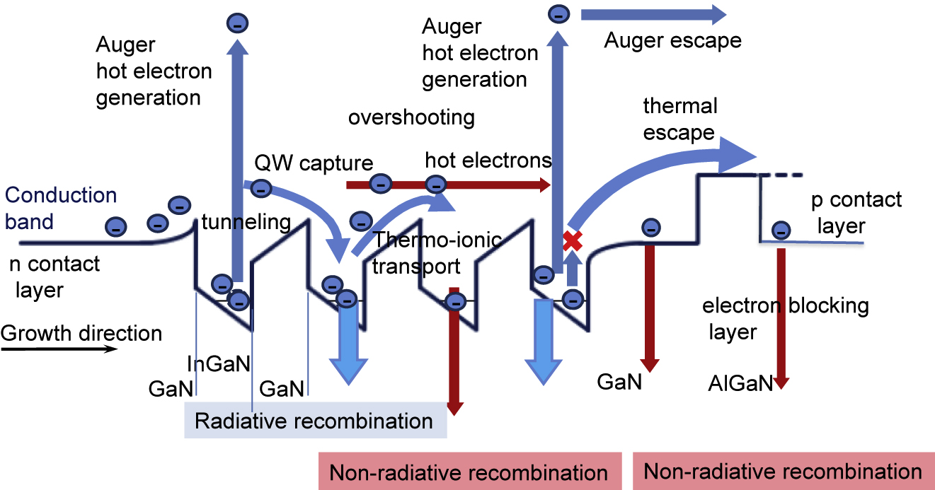
Schematics of the phenomena occurring in LEDs best captured by nonequilibrium computing techniques such as NEGF or Monte Carlo.
We note that alloy disorder, so far, is missing from the NEFG simulations. NEGF computations taking alloy disorder into account would be a 4D problem (
Another way to treat the hot carrier effects absent in DD simulation is the Monte Carlo method. In the computations by Kivisaari et al., they however do not solve the discrepancy of larger VF than observed, in particular for green LEDs, with excess VF from 1 to 2.7 V for 3 or 8 QW LEDs, respectively [88]. Another computation of hot electron effects solves numerically the electron Boltzmann transport equation in the MQW region by assuming a voltage drop of 3 V over the QW stack [89]. With such voltage drop, significant carrier escape out of the active region into the p-contact layer is predicted, arguing that this is a cause for droop, the large excess voltage implied does not represent the VF of commercial LEDs.
9 Modeling the disordered potential induced by alloy compositional fluctuations
We mentioned that due to the large differences in atom potentials in InGaN, the effects of alloy disorder will be strong and that the usual VCA used for the common III–V alloys is insufficient for simulations of nitrides [90], [91], [92]. One then needs to compute the local energy levels entering the simulation equations.
Some groups compute the energy levels from first principles, usually TB approximation [74], [93] in supercells with random In atom positions that are supposed to represent the alloy at larger scales. The supercell size is clearly a limiting factor (we however note that Tanner et al. used 81,920 atoms in their supercell [94]) and to ensure the reliability of the procedure, many different random supercell configurations are computed, and the final result is the averaged results over the configurations that exhibit sizeable differences (see, e.g., Figure 3 in the study by Tanner et al. [74]).
Many other groups [14], [34], [95], [96] compute energy levels in two steps: they first compute the disordered potential map Ve,h (x, y, z) acting on carriers using the EMA, and then compute the energy levels by solving the Schrödinger equation of the carrier envelope wave function. One uses the fact that the potential varies smoothly at the atomic length scale to approximate the local potential as the bandgap of the bulk alloy with the local composition. This is the easiest approach to grasp the impact of compositional disorder.
In this approach, a first input to simulations is the generation of a compositional map of the disordered alloy, performed by connecting the discrete quantized atom composition as measured by APT, or from a random number generator, to a continuous variation by weighting each site composition with a continuous Gaussian function (Figure 7a). The standard variation σ is usually taken as twice the lattice constant a (a = 2.833 Å). This choice of weighting is dictated by having a continuous composition that represents a physically meaningful fluctuating compositional map. Too small a σ would lead to maps with very large fluctuations, and too large a σ would average compositional fluctuations. The value σ = 2a is commonly used [14], [34], [92], [95]. This approach is questioned as empirical by Di Vito et al. [97] who compare the various approaches of construction of the compositional map. Let us recall here the arguments for this choice given in the study by Li et al. [14]. First, such an averaging length scale 2σ can be extracted from the results of the energy maps and effective energy maps (see, e.g., Figures 7c and 8b): the latter provide the effective potential fluctuations for charge carriers, and, as well as the energy maps, display variations over characteristic lengths of a few nm, quite larger than 2σ, which justifies that the chosen averaging length scale does capture the smaller scale fluctuations. However, this could be seen as a circular argument. A more fundamental argument obtained from a general theory of disorder [98] is given in the study by Li et al. [14].
![Figure 7: Construction of the potential map seen by electrons; (a) Gaussian averaging of In composition; (b) resulting compositional map in the middle of an In0,14Ga0.86N QW; (c) potential map of conduction electrons. Energy counted from the bottom of the band (from the study by Li et al. [14]).](/document/doi/10.1515/nanoph-2020-0590/asset/graphic/j_nanoph-2020-0590_fig_007.jpg)
Construction of the potential map seen by electrons; (a) Gaussian averaging of In composition; (b) resulting compositional map in the middle of an In0,14Ga0.86N QW; (c) potential map of conduction electrons. Energy counted from the bottom of the band (from the study by Li et al. [14]).
![Figure 8: (a) Spatial variation of the conduction band minimum Ec(r) for a random In0,14Ga0.86N alloy and (b) the effective potential map 1/ue(r) computed through the LL theory; (c) a cut across the x-direction allows comparisons of the fluctuations of both potentials. One can see that energy fluctuations are quite diminished in the LL theory as it captures two essential ingredients of quantum theory: quantum confinement and tunneling (from the study by Li et al. [14]).](/document/doi/10.1515/nanoph-2020-0590/asset/graphic/j_nanoph-2020-0590_fig_008.jpg)
(a) Spatial variation of the conduction band minimum Ec(r) for a random In0,14Ga0.86N alloy and (b) the effective potential map 1/ue(r) computed through the LL theory; (c) a cut across the x-direction allows comparisons of the fluctuations of both potentials. One can see that energy fluctuations are quite diminished in the LL theory as it captures two essential ingredients of quantum theory: quantum confinement and tunneling (from the study by Li et al. [14]).
Knowing the compositional map, one generates maps of energy band extrema Ec(r) and Ev(r) from the bandgap variation given by the bowing parameter, using a 63/37% ratio of conduction band and valence band offsets (Figure 6b). The bowing parameter b describes the quadratic variation of bandgap with alloying as follows:
For TB computations of supercells, the evaluation of the bowing parameter is unclear. In the most detailed article by Caro et al. [99], the bowing parameter depends on composition, with most of the changes in the conduction band, quite a contrast with the approximation made in EMA computations that split the energy variations 63%/37% in the conduction band and valence band, respectively.
Tanner et al. [94] compared the TB and EMA approaches and found similar results for peak energies and PL FWHM (the differences reported in Table I of the study by Tanner et al. [94] is mainly due to the different QW thicknesses used in the two types of simulations). It should be noted that the reasonably good agreement with experiment assumes QW thickness fluctuations of 2 monolayers [94].
Additional ingredients to generate the 3D band maps are the effects of internal fields due to spontaneous and piezoelectric fields [14], [93], [94], [99] and the vertical potential map. The vertical compositional variation in QWs is added through a function representing the vertical In atom distribution. A simplifying approximation is to use a Gaussian distribution with width σ = 2a, which approximates quite well the vertical variation of In composition [101], however, with a misrepresentation of the asymmetric top and bottom interface roughness.
Having the potential maps for the conduction and valence bands taking disorder into account, all properties can in principle be readily computed in the EMA approximation. As in nitrides, the energy fluctuations are in the tens of meV range and the spatial compositional variations in the few nm length scale (Figure 7c), both lead to strong quantum effects (see Figure 8c). Thus, before computing materials and device properties, one needs to compute carrier energy levels quantum mechanically in a disordered material by solving the Schrödinger equation for carriers in the disordered potential.
10 Simulations of optical spectra
There are now quite a few simulations of energy levels, absorption and emission of QWs that include disorder effects (without disorder, predictions are poor as the band tails play an important role in the absorption edge and emission wavelength). The impact of disorder is calculated with energy maps obtained either from first principle TB [92], [93], [97] or from the EMA [14], [92], [93], [96], followed by solving the Schrödinger equations for electrons or holes in their respective disordered potential, or by solving the approximate landscape equations (see the following sections) [14], [34], [96]. The resulting energy levels are used to predict optical properties such as absorption, luminescence, … These calculations are extremely demanding on computing resources, the number of mesh nodes in finite-element computations exceeding a few ∼105 for typical QWs.
An obvious expectation from such simulations is the prediction of absorption and luminescence and of the resulting Stokes shift [32], [95], [102], [103].
To simulate the situation in electrically injected QWs in an LED under bias, a carrier density is numerically injected in a QW structure, with the internal electric fields further computed self-consistently. Another approach relies on the computation, in a tractable 1D self-consistent LED model, of the potentials, the electric fields and the carrier densities, which are then used in 3D Schrödinger computations of optical properties without any further attempt to self-consistency.
Even including alloy disorder, there are still significant discrepancies between simulations and experiments for the dependence of the emission wavelength on In contents and QW thickness: at high In contents beyond blue emission, the simulated emission wavelength differs significantly from the simulated wavelength. For green LEDs, green (525 nm) emission is experimentally obtained with 24% of In for 3-nm-thick QWs while computations require ≈30% In to reach green wavelengths in 1D simulation software, advanced 1D NEGF or 3D computations [87], [91].
To reconciliate measurements and simulations, one can invoke large interface roughness [35] or QW thickness fluctuations. The discrepancy could be alternatively linked to the use of a too small bowing parameter b, which would then underestimate the size of energy fluctuations (one usually takes b = −1.4 eV, whereas some computations point to much larger values [99]). Electron-hole interactions should also always be included as they lead to redshifts of the order of 50 meV [32] or 30–40 meV [74].
Another optical probe of disorder is the onset of the absorption curve, so-called Urbach tail, which follows an exponential dependence on energy. In InGaN MQW solar-cell structures designed for photo-carrier collection, it was shown that the exponential slope is mainly determined by the compositional fluctuations induced by alloy disorder [34]. Using the LL theory (see the following sections), it was shown that the slope is ∼25–35 meV for In content in the range of 11–28%, in reasonable agreement with the ∼20 meV of experiment. Direct computations from solving the time-dependent Schrödinger equation [32] found ∼20 meV, however, only when taking e–h Coulomb interaction into account, vs. 7 meV when ignoring Coulomb interaction.
A significant result of the direct Schrödinger computations is the weaker or nonexistent localization of electrons due to their light effective mass in contrast with the strong localization of holes [74], [95], [97]. As mentioned previously, this is a topic for further investigation of electron transport at low temperatures. For optical properties, this could however be somewhat modified in interband transitions by the e–h interaction that could localize electrons because of their interaction with a localized hole [74], [104].
11 Simulations of the ABC recombination parameters
The determination of the recombination parameters A, B and C allows to model the IQE, droop, the green gap. Together with transport properties, they play a major role in predicting electrical properties in their interaction with optical phenomena in full LED structures, as recombination is a very dominant phenomenon in the carrier transport through LED structures [105].
Although B and C are intrinsic parameters that can be computed from materials and structure modeling, A is connected to NR mechanisms most often associated with defects. In some cases, the A coefficient depends on the vertical e–h wave function overlap, therefore on bias and injected current, and should be simulated, as done by David et al. [8].
As B and C vary so much with structures, good simulations of measured values are needed to further have a good simulation tool. B is critical, giving the radiative efficiency. The effect of the internal field separating the electron and holes and the disorder-induced in-plane different electron and hole localizations both affect the e–h wave function overlap [32].
Since the first observations of droop, the C coefficient has been the subject of intense scrutiny. Even when Auger recombination was rather convincingly demonstrated in 2007, doubts arose as the Auger coefficient deduced from experiments was considered unphysically high [55].
Then, two questions arose: (1) which other processes lead to a carrier loss with a similar carrier-density dependence as Auger; (2) can one predict Auger coefficients of the correct magnitude? The main mechanism invoked besides Auger NR recombination is carrier escape from the active region. Experimental evidence was shown to be disputable [61], [63] and theoretical support further discussed in the LED simulation section shows it to be negligible.
Several effects increase the direct Auger coefficient computed within the VCA, that is, without disorder, ≈3.10−34–10−35 cm6 s−1, either due to phonon- or disorder-assistance which both relax the k-conservation rule responsible for the very small direct Auger coefficient in wide-bandgap materials [65]. They however rely on the use of 100–300 meV broadening parameter. Another phenomenon which partially relaxes the k-conservation rule is the finite thickness of the QW, which increases C [59], while the internal fields decrease C due to the e–h wave function separations [58]. However, the analysis (without disorder effects) predicts an oscillatory behavior of the Auger rate with QW thickness which has not been observed [59]. From the absence of significant Auger recombination in GaN QWs, beyond the effect of increased bandgap, one concludes that disorder must play a major role in the large Auger coefficient with computed values in the right order of magnitude [65], [106].
A missing item of most B and C simulations is the e–h Coulomb interaction. Although no hydrogen-like relative motion of the e–h pairs is expected because of the diminished e–h overlap due to QCSE and to the localizing potentials that destroy the e-h correlated relative motion [107], the e–h Coulomb interaction leads to an increased optical matrix element (similar to the Sommerfeld factor in unbound hydrogenic states [108]) observed and computed by David et al. [32], [49], with a significant increase of B compared with noninteracting e–h pairs.
12 LED modeling taking disorder into account
As mentioned previously, LED simulations do not include disorder fail to account for a well-measured parameter, the forward voltage VF. Using the ad hoc diminished internal field yields correct voltages, but other quantities such as the QCSE and wave functions overlaps yield incorrect values.
There is so far only one LED simulation tool taking disorder into account. This is due to the hugely increased required computational power, well beyond that required for optical properties: one needs to add a module for carrier transport to the computation of optical properties. But, and the most important, as one wishes to simulate I–V curves and dependence of the electrical-to-optical conversion on current injection, one will need to compute for a large number of different diode bias voltages and also to run self-consistent loops to account for the modifications of the internal field maps due to injected carriers. A self-consistent loop takes 20 roundtrips to converge on average [14]; thus, one needs at least 500 more time to compute an LED than the optical simulation alone, neglecting the additional time required to solve the DD equations (indeed small, see Figure 5c). Given that computing the optical properties through the Schrödinger equation takes about a day, computing one LED structure would take 500+ days (Figure 5c on computing times).
The tool is based on an approximate solution to the Schrödinger equation in the EMA approximation based on the Filoche–Mayboroda 3D LL theory, which from the original disordered energy map provides an effective potential that allows the use of the standard DD transport equations while accounting for microscopic disorder [109].
The Schrödinger equation is replaced by the landscape equation:
where
The use of the landscape equation in lieu of Schrödinger’s equation leads to a remarkable gain of 103 in computing speed, making 3D self-consistent computations possible based on a finite element method computational approach [14], [110]. The electro-optical behavior of LEDs is simulated by self-consistently solving the Poisson, landscape, and DD equations in 3D structures (Figure 5b). Details of the theory are given in the studies by Li et al. and Wu et al. [14], [110]. Simulations use 100% of the known values for the spontaneous and piezoelectric polarization parameters. As no model exists yet of the electric transport parameters with hopping phenomena (however, strongly suppressed under the carrier densities under LED operation where localized states should be filled), ones uses available DD parameters. In the same vein, one uses A, B and C parameters from the literature, however, choosing their value nearest to those of the disorder-less alloy (see the discussion on the choice of parameters in the study by Li et al. [14]). A better choice might be those determined in the VCA approximation. Simulations of the blue six QW LED of Figure 2a are shown in Figure 9. The strain and polarization fields (spontaneous and piezoelectric) are calculated before entering the self-consistency loop [14].
![Figure 9: Computations of the six QW LED of Figure 2a.(a) Computed I–V curves: dashed black curve: classical Poisson-DD equations assuming full polarization in the LED structure; red curve: Poisson-DD equations with classical treatment of disorder (meaning one uses in the DD equations the computed disordered potential directly obtained from compositional fluctuations without computing the quantum corrections by solving the Schrödinger equation of carriers in the disordered potential); full black curve: no disorder, classical Poisson-DD equations assuming 50% polarization; blue curve: LL theory treatment of disorder with classical Poisson-DD equations; (b) computed self-consistent in-plane electron density in the mid-plane of the third QW with compositional disorder using: (left) the classical disorder, Poisson and DD models; (right) the LL effective potential, Poisson and DD models; (c) recombination currents in each of the 6 QW, displaying the large injection inhomogeneity, which is partly the source of large droop due to the high carrier concentration in the 6th QW (top, p-side QW); (d) LL theory implemented in Poisson-DD LED model. Perspective views of the LL function (1/ue) and of the normal component of current (Jz) calculated for an MQW LED in the midplane (x–y plane) of the third QW. Figures in panels b, c and d are solved by 1/u-Poisson-DD model, where the LED current density is 20 A cm−2 (from the study by Li et al. [14]).](/document/doi/10.1515/nanoph-2020-0590/asset/graphic/j_nanoph-2020-0590_fig_009.jpg)
Computations of the six QW LED of Figure 2a.
(a) Computed I–V curves: dashed black curve: classical Poisson-DD equations assuming full polarization in the LED structure; red curve: Poisson-DD equations with classical treatment of disorder (meaning one uses in the DD equations the computed disordered potential directly obtained from compositional fluctuations without computing the quantum corrections by solving the Schrödinger equation of carriers in the disordered potential); full black curve: no disorder, classical Poisson-DD equations assuming 50% polarization; blue curve: LL theory treatment of disorder with classical Poisson-DD equations; (b) computed self-consistent in-plane electron density in the mid-plane of the third QW with compositional disorder using: (left) the classical disorder, Poisson and DD models; (right) the LL effective potential, Poisson and DD models; (c) recombination currents in each of the 6 QW, displaying the large injection inhomogeneity, which is partly the source of large droop due to the high carrier concentration in the 6th QW (top, p-side QW); (d) LL theory implemented in Poisson-DD LED model. Perspective views of the LL function (1/ue) and of the normal component of current (Jz) calculated for an MQW LED in the midplane (x–y plane) of the third QW. Figures in panels b, c and d are solved by 1/u-Poisson-DD model, where the LED current density is 20 A cm−2 (from the study by Li et al. [14]).
As can be seen in Figure 9a, the LL computation gives a correct LED forward voltage for blue LEDs without any adjustment of parameters, about 3 V at 20 A/cm2 vs. an experimental 2.8 V for the better commercial LEDs. The small difference might come from the approximate vertical alloy composition map. The lowering of onset diode voltage compared with simulations without disorder is due to carriers being transported preferentially through regions of lower effective bandgap induced by disorder. The current through the LED structure undergoes complex trajectories, similar to percolation paths in disordered systems, as carriers transport in the perpendicular directions to QW planes through regions where energy barriers are easier to surpass. They will also relax in the QW plane in the domains of lower energies (Figure 9d) [14], [101]. These paths, which can only be simulated in 3D computations, lead to these values of VF in good agreement with measured values for blue LEDs, without having to modify the polarization parameters such as in 1D models. Disorder of course leads to carrier concentration in the high In contents, low energy regions, and one can clearly see the smoothing action of the quantum computation of effective potential (Figure 9b). One also recovers the hole transport mostly limited to the p side of MQW LED structures as shown by the concentration of recombination density in the QW nearest to the LED p-side (Figure 9c). Among the additional results are the confirmation of (1) unequal injection among the MQWs; (2) the enhancement of Auger-induced droop because of the enhanced carrier concentrations in lower energy regions [14]; and (3) carrier escape being negligible for LED current densities, pointing to the dominant role of Auger NR recombination as the cause for droop through simulation.
The 3D simulations, based on the LL theory, work surprisingly well for blue LEDs given some of the very rough approximations: the absence of vertical QW-to-QW tunneling, DD model of carrier transport instead of accounting for disorder-dominated transport. This is quite certainly due to the fact that the parameters used in the simulations implicitly include the effects of disorder: recombination parameters A, B and C, carrier mobilities, bowing parameter, …
The LL modeling also provides insight on the green gap. The green gap is due to two factors, the diminished EQE and the excess voltage ΔVF needed in longer wavelength MQW LEDs. Let us define ΔVF. As mentioned previously, the onset voltage VF is set by the e–h recombination energy hν. This is indeed the case for blue and shorter wavelength LEDs, but for green and longer wavelength LEDs the excess voltage ΔVF = VF − Vph (where eVph = hν) can reach 0.4 V per QW in the sequence of MQWs, which translates into loss of efficiency, the emitted energy per e–h pair still being the photon energy. Recent modeling through the LL theory pointed to the excess voltage being due to both increased internal fields and band discontinuities with In concentration, which impede the usual carrier transport from well to well and call for larger bias voltages [111], [112]. This indicates that mitigation of the excess voltage implies diminishing internal energy barriers through doping [21] or alloying, or more radically through injecting carrier laterally to prevent the required cascade of carriers through the multiple barriers in vertically injected MQW LEDs. This has been successfully achieved using V defects as lateral injectors [113].
For completeness sake, even this 3D model including disorder fails to capture two important parameters of green LEDs: the computed VF is too high by about 0.2 V for an SQW LED and by 1 V for a 7 QW LED [111], and the wavelength for a typical experimental In concentration of 24% is too short by about 30 nm compared with the experiment. Several explanations have been invoked for the latter beyond the early-invoked large Stokes shift increasing nonlinearly with In concentration [23], disputable as discussed previously. Other possible causes are large interface roughness or QW thickness fluctuations, the use of a too small bowing parameter to describe the variation of the bandgap with In concentration. Missing items could also the use of a simplified, symmetric vertical In atom distribution and the neglect of Coulomb interactions.
Solutions to resolve the excess voltage contribution to the green gap, other than V defects lateral injectors involve using doping of barrier materials do compensate the internal fields [21] or using alloy barriers to diminish the energy barrier to carrier transport throughout the structures. The optimization of such structures, or any other mitigation solution, will require precise full 3D modeling of LEDs.
13 Conclusion
One can see that, while computing optical properties is within reach provided some “educated” guesses on the structure geometries, on carrier thermalization, and so forth, are made, computing full LED device structures is a much more formidable task, given the required computing resources and the lack of detailed transport mechanisms that properly treat alloy disorder effects. While the LL theory markedly reduces the computation time, it still lacks a way to incorporate the out-of-equilibrium phenomena solved by the NEGF technique. Unfortunately, it appears that putting together LL and NEGF computations becomes again a too formidable task to compute. There is clearly a need for new ideas to make the field of LED simulations tractable.
One general remark on the disappointing state of understanding nitride structures is other semiconductor materials such as Ge or Si, or other III–Vs, required long efforts to achieve their full potential. The excellent early results of nitride devices may have hampered the funding resources, and thus the efforts required for a full understanding of this very interesting, specific and rather intriguing materials system. Indeed, with blue LEDs operating at energy conversion efficiency greater than 80% at low current densities, it did not seem obvious that better understanding of structures and device physics would yield clear improvements. We of course believe that it is not so, in view of the need to solve the two major limitations of nitride LEDs, the green gap and the “droop” in efficiency.
Funding source: U.S. Department of Energy
Award Identifier / Grant number: DE-EE0008204
Funding source: National Science Foundation
Award Identifier / Grant number: 1839077
Funding source: Simons Foundation
Award Identifier / Grant number: 601952
Award Identifier / Grant number: 601954
Funding source: Ministry of Science and Technology in Taiwan
Award Identifier / Grant number: MOST 108-2628-E-002-010-MY3
Acknowledgments
The authors acknowledge funding from the Solid State Lighting and Energy Electronics Center (SSLEEC) at the University of California, Santa Barbara (UCSB). C.W. thanks Aurélien David for many illuminating discussions and, with Pierre Petroff and Jacques Peretti, for a critical reading of the manuscript.
Author contribution: All the authors have accepted responsibility for the entire content of this submitted manuscript and approved submission.
Research funding: This work was supported by the U.S. Department of Energy under Award No. DE-EE0008204, supported by the National Science Foundation under award # 1839077 (through a subcontract from the University Minnesota), grants from the Simons Foundation (601952, J.S.), (601954, C.W.) and by the Ministry of Science and Technology in Taiwan under Grant No. MOST 108-2628-E-002-010-MY3.
Conflict of interest statement: The authors declare no conflicts of interest regarding this article.
References
[1] B. I. Shklovskii and A. L. Efros, Electronic Properties of Doped Semiconductors, Springer Berlin Heidelberg, 1984.10.1007/978-3-662-02403-4Suche in Google Scholar
[2] E. C. Young, N. Grandjean, T. E. Mates, and J. S. Speck, “Calcium impurity as a source of non-radiative recombination in (In,Ga)N layers grown by molecular beam epitaxy,” Appl. Phys. Lett., vol. 109, p. 212103, 2016. https://doi.org/10.1063/1.4968586.Suche in Google Scholar
[3] C. Haller, J. F. Carlin, G. Jacopin, D. Martin, R. Butté, and N. Grandjean, “Burying non-radiative defects in InGaN underlayer to increase InGaN/GaN quantum well efficiency,” Appl. Phys. Lett., vol. 111, p. 262101, 2017. https://doi.org/10.1063/1.5007616.Suche in Google Scholar
[4] C. Haller, J. F. Carlin, G. Jacopin, et al.., “GaN surface as the source of non-radiative defects in InGaN/GaN quantum wells,” Appl. Phys. Lett., vol. 113, pp. 1–5, 2018. https://doi.org/10.1063/1.5048010.https://doi.org/10.1063/1.5048010Suche in Google Scholar
[5] A. C. Espenlaub, D. J. Myers, E. C. Young, S. Marcinkevičius, C. Weisbuch, and J. S. Speck, “Evidence of trap-assisted Auger recombination in low radiative efficiency MBE-grown III-nitride LEDs,” J. Appl. Phys., vol. 126, p. 184502, 2019. https://doi.org/10.1063/1.5096773.Suche in Google Scholar
[6] D. J. Myers, K. GelŽinytė, A. I. Alhassan, et al.., “Direct measurement of hot-carrier generation in a semiconductor barrier heterostructure: identification of the dominant mechanism for thermal droop,” Phys. Rev. B, vol. 100, p. 125303, 2019. https://doi.org/10.1103/physrevb.100.125303.Suche in Google Scholar
[7] A. David, N. G. Young, C. A. Hurni, and M. D. Craven, “Quantum efficiency of III-nitride emitters: evidence for defect-assisted nonradiative recombination and its effect on the green gap,” Phys. Rev. Appl., vol. 11, p. 031001, 2019. https://doi.org/10.1103/physrevapplied.11.031001.Suche in Google Scholar
[8] A. David, G. Young Nathan, C. Lund, and M. D. Craven, “Compensation between radiative and Auger recombinations in III-nitrides: the scaling law of separated-wavefunction recombinations,” Appl. Phys. Lett., vol. 115, p. 193502, 2019. https://doi.org/10.1063/1.5123743.Suche in Google Scholar
[9] P. Sohi, J. F. Carlin, and N. Grandjean, “Alloy disorder limited mobility of InGaN two-dimensional electron gas,” Appl. Phys. Lett., vol. 112, p. 262101, 2018. https://doi.org/10.1063/1.5030992.Suche in Google Scholar
[10] D. N. Nath, Z. C. Yang, C. Y. Lee, P. S. Park, Y. R. Wu, and S. Rajan, “Unipolar vertical transport in GaN/AlGaN/GaN heterostructures,” Appl. Phys. Lett., vol. 103, p. 022102, 2013. https://doi.org/10.1063/1.4813309.Suche in Google Scholar
[11] D. A. Browne, B. Mazumder, Y. R. Wu, and J. S. Speck, “Electron transport in unipolar InGaN/GaN multiple quantum well structures grown by NH3 molecular beam epitaxy,” J. Appl. Phys., vol. 117, p. 185703, 2015. https://doi.org/10.1063/1.4919750.Suche in Google Scholar
[12] K. S. Qwah, M. Monavarian, G. Lheureux, J. Wang, Y. R. Wu, and J. S. Speck, “Theoretical and experimental investigations of vertical hole transport through unipolar AlGaN structures: impacts of random alloy disorder,” Appl. Phys. Lett., vol. 117, p. 022107, 2020. https://doi.org/10.1063/5.0006291.Suche in Google Scholar
[13] U. S. Dep. Energy, “2018 Solid-State Lighting R & D Opportunities,” 2019, Available at https://www.energy.gov/sites/prod/files/2019/02/f59/edit.ssl_rd-opportunities_jan2019.pdf [accessed: Oct. 31, 2020].Suche in Google Scholar
[14] C. K. Li, M. Piccardo, L. S. Lu, et al.., “Localization landscape theory of disorder in semiconductors. III. Application to carrier transport and recombination in light emitting diodes,” Phys. Rev. B, vol. 95, p. 144206, 2017. https://doi.org/10.1103/physrevb.95.144206.Suche in Google Scholar
[15] S. De, A. Layek, A. Raja, et al.., “Two distinct origins of highly localized luminescent centers within InGaN/GaN quantum-well light-emitting diodes,” Adv. Funct. Mater., vol. 21, pp. 3828–3835, 2011. https://doi.org/10.1002/adfm.201100894.Suche in Google Scholar
[16] M. Mensi, R. Ivanov, T. K. Uždavinys, et al.., “Direct measurement of nanoscale lateral carrier diffusion: toward scanning diffusion microscopy,” ACS Photonics, vol. 5, pp. 528–534, 2018. https://doi.org/10.1021/acsphotonics.7b01061.Suche in Google Scholar
[17] S. Sonderegger, E. Feltin, M. Merano, et al.., “High spatial resolution picosecond cathodoluminescence of InGaN quantum wells,” Appl. Phys. Lett., vol. 89, p. 232109, 2006. https://doi.org/10.1063/1.2397562.Suche in Google Scholar
[18] T. K. Uždavinys, S. Marcinkevičius, M. Mensi, et al.., “Impact of surface morphology on the properties of light emission in InGaN epilayers,” Appl. Phys. Express, vol. 11, p. 051004, 2018.10.7567/APEX.11.051004Suche in Google Scholar
[19] W. Hahn, J. M. Lentali, P. Polovodov, et al.., “Evidence of nanoscale Anderson localization induced by intrinsic compositional disorder in InGaN/GaN quantum wells by scanning tunneling luminescence spectroscopy,” Phys. Rev. B, vol. 98, p. 045305, 2018. https://doi.org/10.1103/physrevb.98.045305.Suche in Google Scholar
[20] G. Callsen, R. Butté, and N. Grandjean, “Probing alloy formation using different excitonic species: the particular case of InGaN,” Phys. Rev. X, vol. 9, p. 031030, 2019. https://doi.org/10.1103/physrevx.9.031030.Suche in Google Scholar
[21] N. G. Young, R. M. Farrell, S. Oh, et al.., “Polarization field screening in thick (0001) InGaN/GaN single quantum well light-emitting diodes,” Appl. Phys. Lett., vol. 108, p. 061105, 2016. https://doi.org/10.1063/1.4941815.Suche in Google Scholar
[22] S. Srinivasan, F. Bertram, A. Bell, et al.., “Low Stokes shift in thick and homogeneous InGaN epilayers,” Appl. Phys. Lett., vol. 80, pp. 550–552, 2002. https://doi.org/10.1063/1.1436531.Suche in Google Scholar
[23] R. W. Martin, P. G. Middleton, K. P. O’Donnell, and W. Van Der Stricht, “Exciton localization and the Stokes’ shift in InGaN epilayers,” Appl. Phys. Lett., vol. 74, pp. 263–265, 1999. https://doi.org/10.1063/1.123275.Suche in Google Scholar
[24] M. Meneghini, C. De Santi, A. Tibaldi, et al.., “Thermal droop in III-nitride based light-emitting diodes: physical origin and perspectives,” J. Appl. Phys., vol. 127, p. 211102, 2020. https://doi.org/10.1063/5.0005874.Suche in Google Scholar
[25] K. P. O’Donnell, R. W. Martin, and P. G. Middleton, “Origin of luminescence from InGaN diodes,” Phys. Rev. Lett., vol. 82, pp. 237–240, 1999. https://doi.org/10.1103/physrevlett.82.237.Suche in Google Scholar
[26] E. Berkowicz, D. Gershoni, G. Bahir, A. C. Abare, S. P. DenBaars, and L. A. Coldren, “Optical spectroscopy of InGaN/GaN quantum wells,” Phys. Status Solidi Basic Res., vol. 216, pp. 291–300, 1999. https://doi.org/10.1002/(sici)1521-3951(199911)216:1<291::aid-pssb291>3.0.co;2-o.10.1002/(SICI)1521-3951(199911)216:1<291::AID-PSSB291>3.0.CO;2-OSuche in Google Scholar
[27] S. F. Chichibu, T. Sota, K. Wada, S. P. DenBaars, and S. Nakamura, “Spectroscopic studies in InGaN quantum wells,” MRS Internet J. Nitride Semicond. Res., vol. 4, pp. 93–105, 1999. https://doi.org/10.1557/S1092578300002295.Suche in Google Scholar
[28] F. Nippert, Non-radiative Loss Mechanisms in InGaN/GaN Multiple Quantum Well Light-Emitting Diodes, Thesis, Technical University Berlin, 2017.Suche in Google Scholar
[29] Y. H. Cho, G. H. Gainer, A. J. Fischer, et al.., “‘S-shaped’ temperature-dependent emission shift and carrier dynamics in InGaN/GaN multiple quantum wells,” Appl. Phys. Lett., vol. 73, pp. 1370–1372, 1998. https://doi.org/10.1063/1.122164.Suche in Google Scholar
[30] S. Yang, Y. Liu, Y. Zhang, and D. Mo, “Investigation of annealing-treatment on structural and optical properties of sol–gel-derived zinc oxide thin films,” Bull. Mater. Sci., vol. 33, pp. 209–214, 2010. https://doi.org/10.1007/s12034-010-0032-x.Suche in Google Scholar
[31] A. David and M. J. Grundmann, “Influence of polarization fields on carrier lifetime and recombination rates in InGaN-based light-emitting diodes,” Appl. Phys. Lett., vol. 97, p. 033501, 2010. https://doi.org/10.1063/1.3462916.Suche in Google Scholar
[32] A. David, N. G. Young, and M. D. Craven, “Many-body effects in strongly disordered III-nitride quantum wells: interplay between carrier localization and Coulomb interaction,” Phys. Rev. Appl., vol. 12, p. 044059, 2019. https://doi.org/10.1103/physrevapplied.12.044059.Suche in Google Scholar
[33] J. Tauc, R. Grigorovici, and A. Vancu, “Optical properties and electronic structure of amorphous germanium,” Phys. Status Solidi, vol. 15, pp. 627–637, 1966. https://doi.org/10.1002/pssb.19660150224.Suche in Google Scholar
[34] M. Piccardo, C. K. Li, Y. R. Wu, et al.., “Localization landscape theory of disorder in semiconductors. II. Urbach tails of disordered quantum well layers,” Phys. Rev. B, vol. 95, p. 144205, 2017. https://doi.org/10.1103/physrevb.95.144205.Suche in Google Scholar
[35] D. M. Graham, A. Soltani-Vala, P. Dawson, et al.., “Optical and microstructural studies of InGaNGaN single-quantum-well structures,” J. Appl. Phys., vol. 97, p. 103508, 2005. https://doi.org/10.1063/1.1897070.Suche in Google Scholar
[36] J. Danhof, H. M. Solowan, U. T. Schwarz, et al.., “Lateral charge carrier diffusion in InGaN quantum wells,” Phys. Status Solidi Basic Res., vol. 249, pp. 480–484, 2012. https://doi.org/10.1002/pssb.201100476.Suche in Google Scholar
[37] H. M. Solowan, J. Danhof, and U. T. Schwarz, “Direct observation of charge carrier diffusion and localization in an InGaN multi quantum well,” Jpn. J. Appl. Phys., vol. 52, pp. 08JK07-1–08JK07-5, 2013. https://doi.org/10.7567/jjap.52.08jk07.Suche in Google Scholar
[38] K. Kumakura, T. Makimoto, N. Kobayashi, T. Hashizume, T. Fukui, and H. Hasegawa, “Minority carrier diffusion lengths in MOVPE-grown n- and p-InGaN and performance of AlGaN/InGaN/GaN double heterojunction bipolar transistors,” J. Cryst. Growth, vol. 298, pp. 787–790, 2007. https://doi.org/10.1016/j.jcrysgro.2006.10.098.Suche in Google Scholar
[39] S. Nakamura, M. Senoh, N. Iwasa, and S. Nagahama chi, “High-power InGaN single-quantum-well-structure blue and violet light-emitting diodes,” Appl. Phys. Lett., vol. 67, pp. 1868–1870, 1995. https://doi.org/10.1063/1.114359.Suche in Google Scholar
[40] S. Nakamura and M. R. Krames, “History of gallium-nitride-based light-emitting diodes for illumination,” Proc. IEEE, vol. 101, pp. 2211–2220, 2013. https://doi.org/10.1109/jproc.2013.2274929.Suche in Google Scholar
[41] S. D. Lester, F. A. Ponce, M. G. Craford, and D. A. Steigerwald, “High dislocation densities in high efficiency GaN-based light-emitting diodes,” Appl. Phys. Lett., vol. 66, p. 1249, 1995. https://doi.org/10.1063/1.113252.Suche in Google Scholar
[42] T. D. Moustakas, “The role of extended defects on the performance of optoelectronic devices in nitride semiconductors,” Phys. Status Solidi Appl. Mater. Sci., vol. 210, pp. 169–174, 2013. https://doi.org/10.1002/pssa.201200561.Suche in Google Scholar
[43] M. Meneghini, G. Meneghesso, and E. Zanoni, Electrical Properties, Reliability Issues, and ESD Robustness of InGaN-Based LEDs. Topics in Applied Physics, vol. 133, Springer Verlag, 2017, pp. 363–395.10.1007/978-981-10-3755-9_13Suche in Google Scholar
[44] A. Hangleiter, F. Hitzel, C. Netzel, et al.., “Suppression of nonradiative recombination by V-shaped pits in GaInN/GaN quantum wells produces a large increase in the light emission efficiency,” Phys. Rev. Lett., vol. 95, p. 127402, 2005. https://doi.org/10.1103/physrevlett.95.127402.Suche in Google Scholar
[45] F. Jiang, J. Zhang, L. Xu, et al.., “Efficient InGaN-based yellow-light-emitting diodes,” Photonics Res., vol. 7, p. 144, 2019.10.1364/PRJ.7.000144Suche in Google Scholar
[46] J. S. Speck and S. J. Rosner, “The role of threading dislocations in the physical properties of GaN and its alloys,” Physica B, vols. 273–274, pp. 24–32, 1999. https://doi.org/10.1016/s0921-4526(99)00399-3.Suche in Google Scholar
[47] S. F. Chichibu, A. Uedono, T. Onuma, et al.., “Origin of defect-insensitive emission probability in In-containing (Al,In,Ga)N alloy semiconductors,” Nat. Mater., vol. 5, pp. 810–816, 2006. https://doi.org/10.1038/nmat1726.Suche in Google Scholar
[48] J. Danhof, H. M. Solowan, U. T. Schwarz, et al.., “Lateral charge carrier diffusion in InGaN quantum wells,” Phys. Status Solidi Basic Res., vol. 249, pp. 480–484, 2012. https://doi.org/10.1002/pssb.201100476.Suche in Google Scholar
[49] A. David, N. G. Young, C. Lund, and M. D. Craven, “Review—the physics of recombinations in III-nitride emitters,” ECS J. Solid State Sci. Technol., vol. 9, p. 016021, 2020. https://doi.org/10.1149/2.0372001jss.Suche in Google Scholar
[50] A. David and C. A. Y. N. Hurni, “High efficiency group-III nitride light emitting diode,” U.S. Patent 10,734,549, 2020.Suche in Google Scholar
[51] C. Weisbuch, M. Piccardo, L. Martinelli, J. Iveland, J. Peretti, and J. S. Speck, “The efficiency challenge of nitride light-emitting diodes for lighting,” Phys. Status Solidi Appl. Mater. Sci., vol. 212, pp. 899–913, 2015. https://doi.org/10.1002/pssa.201431868.Suche in Google Scholar
[52] Y.-R. W. Chi-Kang Li, “Study on the current spreading effect and light extraction enhancement of,” IEEE Trans. Electron. Devices, vol. 59, pp. 400–407, 2012. https://doi.org/10.1109/ted.2011.2176132.Suche in Google Scholar
[53] I. V. Rozhansky and D. A. Zakheim, “Analysis of processes limiting quantum efficiency of AlGaInN LEDs at high pumping,” Phys. Status Solidi Appl. Mater. Sci., vol. 204, pp. 227–230, 2007. https://doi.org/10.1002/pssa.200673567.Suche in Google Scholar
[54] Y. C. Shen, G. O. Mueller, S. Watanabe, N. F. Gardner, A. Munkholm, and M. R. Krames, “Auger recombination in InGaN measured by photoluminescence,” Appl. Phys. Lett., vol. 91, p. 141101, 2007. https://doi.org/10.1063/1.2785135.Suche in Google Scholar
[55] K. A. Bulashevich and S. Y. Karpov, “Is Auger recombination responsible for the efficiency rollover in III-nitride light-emitting diodes?,” Phys. Status Solidi Curr. Top. Solid State Phys., vol. 5, pp. 2066–2069, 2008. https://doi.org/10.1002/pssc.200778414.Suche in Google Scholar
[56] E. Kioupakis, P. Rinke, K. T. Delaney, and C. G. Van De Walle, “Indirect Auger recombination as a cause of efficiency droop in nitride light-emitting diodes,” Appl. Phys. Lett., vol. 98, p. 161107, 2011. https://doi.org/10.1063/1.3570656.Suche in Google Scholar
[57] J. Hader, J. V. Moloney, and S. W. Koch, “Investigation of droop-causing mechanisms in GaN-based devices using fully microscopic many-body theory,” Gall Nitride Mater. Devices VIII, vol. 8625, p. 86251M, 2013.10.1117/12.2005134Suche in Google Scholar
[58] R. Vaxenburg, A. Rodina, E. Lifshitz, and A. L. Efros, “The role of polarization fields in Auger-induced efficiency droop in nitride-based light-emitting diodes,” Appl. Phys. Lett., vol. 103, p. 221111, 2013. https://doi.org/10.1063/1.4833915.Suche in Google Scholar
[59] F. Bertazzi, X. Zhou, M. Goano, G. Ghione, and E. Bellotti, “Auger recombination in InGaN/GaN quantum wells: a full-Brillouin-zone study,” Appl. Phys. Lett., vol. 103, p. 081106, 2013. https://doi.org/10.1063/1.4819129.Suche in Google Scholar
[60] V. Avrutin, S. Hafiz, F. Zhang, et al.., “InGaN light-emitting diodes: efficiency-limiting processes at high injection,” J. Vac. Sci. Technol. A Vac. Surfaces Film, vol. 31, p. 050809, 2013. https://doi.org/10.1116/1.4810789.Suche in Google Scholar
[61] K. J. Vampola, M. Iza, S. Keller, S. P. DenBaars, and S. Nakamura, “Measurement of electron overflow in 450 nm InGaN light-emitting diode structures,” Appl. Phys. Lett., vol. 94, pp. 2–5, 2009. https://doi.org/10.1063/1.3081059.Suche in Google Scholar
[62] M. Deppner, F. Römer, and B. Witzigmann, “Auger carrier leakage in III-nitride quantum-well light emitting diodes,” Phys. Status Solidi Rapid Res. Lett., vol. 6, pp. 418–420, 2012. https://doi.org/10.1002/pssr.201206367.Suche in Google Scholar
[63] A. C. Espenlaub, A. I. Alhassan, S. Nakamura, C. Weisbuch, and J. S. Speck, “Auger-generated hot carrier current in photo-excited forward biased single quantum well blue light emitting diodes,” Appl. Phys. Lett., vol. 112, p. 141106, 2018. https://doi.org/10.1063/1.5021475.Suche in Google Scholar
[64] J. Iveland, L. Martinelli, J. Peretti, J. S. Speck, and C. Weisbuch, “Direct measurement of auger electrons emitted from a semiconductor light-emitting diode under electrical injection: identification of the dominant mechanism for efficiency droop,” Phys. Rev. Lett., vol. 110, p. 177406, 2013. https://doi.org/10.1103/physrevlett.110.177406.Suche in Google Scholar
[65] E. Kioupakis, D. Steiauf, P. Rinke, K. T. Delaney, and C. G. Van De Walle, “First-principles calculations of indirect Auger recombination in nitride semiconductors,” Phys. Rev. B Condens. Matter Mater. Phys., vol. 92, p. 035207, 2015. https://doi.org/10.1103/physrevb.92.035207.Suche in Google Scholar
[66] H. Yoshida, M. Kuwabara, Y. Yamashita, K. Uchiyama, and H. Kan, “Radiative and nonradiative recombination in an ultraviolet GaN/AlGaN multiple-quantum-well laser diode,” Appl. Phys. Lett., vol. 96, p. 211122, 2010. https://doi.org/10.1063/1.3442918.Suche in Google Scholar
[67] M. Shahmohammadi, W. Liu, G. Rossbach, et al.., “Enhancement of Auger recombination induced by carrier localization in InGaN/GaN quantum wells,” Phys. Rev. B, vol. 95, pp. 125314-1–125314-10, 2017. https://doi.org/10.1103/physrevb.95.125314.Suche in Google Scholar
[68] C. Weisbuch, R. Dingle, A. C. Gossard, and W. Wiegmann, “Optical characterization of interface disorder in GaAs-Ga1−xAlxAs multi-quantum well structures,” Solid State Commun., vol. 38, pp. 709–712, 1981. https://doi.org/10.1016/0038-1098(81)90401-4.Suche in Google Scholar
[69] T. Saku, H. Iwamura, Y. Hirayama, Y. Suzuki, and H. Okamoto, “Room temperature operation of 650 nm Algaas multi-quantum-well laser diode grown by molecular beam epitaxy,” Jpn. J. Appl. Phys., vol. 24, pp. L73–L75, 1985. https://doi.org/10.1143/jjap.24.l73.Suche in Google Scholar
[70] J. Hegarty and M. D. Sturge, “Studies of exciton localization in quantum-well structures by nonlinear-optical techniques,” J. Opt. Soc. Am. B, vol. 2, p. 1143, 1985. https://doi.org/10.1364/josab.2.001143.Suche in Google Scholar
[71] S. Chichibu, T. Azuhata, T. Sota, and S. Nakamura, “Luminescences from localized states in InGaN epilayers,” Appl. Phys. Lett., vol. 70, pp. 2822–2824, 1997. https://doi.org/10.1063/1.119013.Suche in Google Scholar
[72] T. M. Smeeton, M. J. Kappers, J. S. Barnard, M. E. Vickers, and C. J. Humphreys, “Electron-beam-induced strain within InGaN quantum wells: false indium ‘cluster’ detection in the transmission electron microscope,” Appl. Phys. Lett., vol. 83, pp. 5419–5421, 2003. https://doi.org/10.1063/1.1636534.Suche in Google Scholar
[73] A. Di Vito, A. Pecchia, A. Di Carlo, and M. Auf der Maur, “Impact of compositional nonuniformity in (In,Ga)N-based light-emitting diodes,” Phys. Rev. Appl., vol. 12, pp. 1–5, 2019. https://doi.org/10.1103/physrevapplied.12.014055.Suche in Google Scholar
[74] D. S. P. Tanner, J. M. McMahon, and S. Schulz, “Interface roughness, carrier localization, and wave function overlap in c-plane (In,Ga)N/GaN quantum wells: interplay of well width, alloy microstructure, structural in homogeneities, and Coulomb effects,” Phys. Rev. Appl., vol. 10, p. 034027, 2018. https://doi.org/10.1103/physrevapplied.10.034027.Suche in Google Scholar
[75] R. A. Oliver, S. E. Bennett, T. Zhu, et al.., “Microstructural origins of localization in InGaN quantum wells,” J. Phys. D Appl. Phys., vol. 43, p. 354003, 2010. https://doi.org/10.1088/0022-3727/43/35/354003.Suche in Google Scholar
[76] P. Dawson, S. Schulz, R. A. Oliver, M. J. Kappers, and C. J. Humphreys, “The nature of carrier localisation in polar and nonpolar InGaN/GaN quantum wells,” J. Appl. Phys., vol. 119, p. 181505, 2016. https://doi.org/10.1063/1.4948237.Suche in Google Scholar
[77] C. Weisbuch, “Review—on the search for efficient Solid state light emitters: past, present, future,” ECS J. Solid State Sci. Technol., vol. 9, p. 016022, 2020. https://doi.org/10.1149/2.0392001jss.Suche in Google Scholar
[78] S. Y. Karpov, “Modeling of III-nitride light-emitting diodes: progress, problems, and perspectives,” Gallium Nitride Mater. Devices VI, vol. 7939, p. 79391C, 2011.10.1117/12.872842Suche in Google Scholar
[79] M. V. Kisin and H. S. El-Ghoroury, “Inhomogeneous injection in III-nitride light emitters with deep multiple quantum wells,” J. Comput. Electron., vol. 14, pp. 432–443, 2015. https://doi.org/10.1007/s10825-015-0673-5.Suche in Google Scholar
[80] J. Geng, P. Sarangapani, K. C. Wang, et al.., “Quantitative multi-scale, multi-physics quantum transport modeling of GaN-based light emitting diodes,” Phys. Status Solidi Appl. Mater. Sci., vol. 215, pp. 1700662-1–1700662-7, 2018. https://doi.org/10.1002/pssa.201700662.Suche in Google Scholar
[81] Z. M. Simon Li and Z. M. S. Li, “Non-local transport in numerical simulation of GaN LED,” J. Comput. Electron., vol. 14, pp. 409–415, 2015. https://doi.org/10.1007/s10825-015-0693-1.Suche in Google Scholar
[82] M. Auf der Maur, “Multiscale approaches for the simulation of InGaN/GaN LEDs,” J. Comput. Electron., vol. 14, pp. 398–408, 2015. https://doi.org/10.1007/s10825-015-0683-3.Suche in Google Scholar
[83] Y. K. Kuo, M. C. Tsai, S. H. Yen, T. C. Hsu, and Y. J. Shen, “Effect of P-type last barrier on efficiency droop of blue InGaN light-emitting diodes,” IEEE J. Quantum Electron., vol. 119, p. 181505, 2010. https://doi.org/10.1063/1.4948237.Suche in Google Scholar
[84] C. Sheng Xia, Z. M. Simon Li, W. Lu, Z. Hua Zhang, Y. Sheng, and L. Wen Cheng, “Droop improvement in blue InGaN/GaN multiple quantum well light-emitting diodes with indium graded last barrier,” Appl. Phys. Lett., vol. 99, p. 233501, 2011. https://doi.org/10.1063/1.3665252.Suche in Google Scholar
[85] D. A. Zakheim, A. S. Pavluchenko, D. A. Bauman, K. A. Bulashevich, O. V. Khokhlev, and S. Y. Karpov, “Efficiency droop suppression in InGaN-based blue LEDs: experiment and numerical modelling,” Phys. Status Solidi Appl. Mater. Sci., vol. 209, pp. 456–460, 2012. https://doi.org/10.1002/pssa.201100317.Suche in Google Scholar
[86] T. Lu, Z. Ma, C. Du, et al.., “Temperature-dependent photoluminescence in light-emitting diodes,” Sci. Rep., vol. 4, p. 6131, 2014. https://doi.org/10.1038/srep06131.Suche in Google Scholar
[87] A. Shedbalkar and B. Witzigmann, “Non equilibrium Green’s function quantum transport for green multi-quantum well nitride light emitting diodes,” Opt. Quantum Electron., vol. 50, no. 67, pp. 1–10, 2018. https://doi.org/10.1007/s11082-018-1335-1.Suche in Google Scholar
[88] P. Kivisaari, T. Sadi, J. Oksanen, and J. Tulkki, “Monte Carlo study of non-quasi equilibrium carrier dynamics in III–N LEDs,” Opt. Quantum Electron., vol. 48, pp. 1–6, 2016. https://doi.org/10.1007/s11082-016-0406-4.Suche in Google Scholar
[89] V. A. Jhalani, J. J. Zhou, and M. Bernardi, “Ultrafast hot carrier dynamics in GaN and its impact on the efficiency droop,” Nano Lett., vol. 17, pp. 5012–5019, 2017. https://doi.org/10.1021/acs.nanolett.7b02212.Suche in Google Scholar
[90] D. P. Nguyen, N. Regnault, R. Ferreira, and G. Bastard, “Alloy effects in Ga1−xInxN/GaN heterostructures,” Solid State Commun., vol. 130, pp. 751–754, 2004. https://doi.org/10.1016/j.ssc.2004.03.048.Suche in Google Scholar
[91] M. Auf Der Maur, A. Pecchia, G. Penazzi, W. Rodrigues, and A. Di Carlo, “Efficiency drop in green InGaN/GaN light emitting diodes: the role of random alloy fluctuations,” Phys. Rev. Lett., vol. 116, pp. 027401-1–027401-5, 2016. https://doi.org/10.1103/physrevlett.116.027401.Suche in Google Scholar
[92] C. M. Jones, C. H. Teng, Q. Yan, P. C. Ku, and E. Kioupakis, “Impact of carrier localization on recombination in InGaN quantum wells and the efficiency of nitride light-emitting diodes: insights from theory and numerical simulations,” Appl. Phys. Lett., vol. 111, p. 113501, 2017. https://doi.org/10.1063/1.5002104.Suche in Google Scholar
[93] S. Schulz, M. A. Caro, C. Coughlan, and E. P. O’Reilly, “Atomistic analysis of the impact of alloy and well-width fluctuations on the electronic and optical properties of InGaN/GaN quantum wells,” Phys. Rev. B Condens. Matter Mater. Phys., vol. 91, p. 035439, 2015. https://doi.org/10.1103/physrevb.91.035439.Suche in Google Scholar
[94] D. S. P. Tanner, P. Dawson, M. J. Kappers, R. A. Oliver, and S. Schulz, “Polar (In,Ga)N/GaN quantum wells: revisiting the impact of carrier localization on the ‘green gap’ problem,” Phys. Rev. Appl., vol. 13, p. 044068, 2020. https://doi.org/10.1103/physrevapplied.13.044068.Suche in Google Scholar
[95] D. Watson-Parris, M. J. Godfrey, P. Dawson, et al.., “Carrier localization mechanisms in InxGa1−xN/GaN quantum wells,” Phys. Rev. B Condens. Matter Mater. Phys., vol. 83, pp. 115321-1–115321-7, 2011. https://doi.org/10.1103/physrevb.83.115321.Suche in Google Scholar
[96] M. Filoche, M. Piccardo, Y. R. Wu, C. K. Li, C. Weisbuch, and S. Mayboroda, “Localization landscape theory of disorder in semiconductors. I. Theory and modeling,” Phys. Rev. B, vol. 95, p. 144204, 2017. https://doi.org/10.1103/physrevb.95.144204.Suche in Google Scholar
[97] A. Di Vito, A. Pecchia, A. Di Carlo, and M. Auf Der Maur, “Simulating random alloy effects in III-nitride light emitting diodes,” J. Appl. Phys., vol. 128, p. 041102, 2020. https://doi.org/10.1063/5.0005862.Suche in Google Scholar
[98] S. D. Baranovskii and A. L. Efros, “Band edge smearing in Solid solutions,” Sov. Phys. Semicond., vol. 12, pp. 1328–1330, 1978.Suche in Google Scholar
[99] M. A. Caro, S. Schulz, and E. P. O’Reilly, “Theory of local electric polarization and its relation to internal strain: impact on polarization potential and electronic properties of group-III nitrides,” Phys. Rev. B Condens. Matter Mater. Phys., vol. 88, p. 214103, 2013. https://doi.org/10.1103/physrevb.88.214103.Suche in Google Scholar
[100] R. Hill, “Energy-gap variations in semiconductor alloys,” J. Phys. C Solid State Phys., vol. 7, pp. 521–526, 1974. https://doi.org/10.1088/0022-3719/7/3/009.Suche in Google Scholar
[101] T.-J. Yang, R. Shivaraman, J. S. Speck, and Y.-R. Wu, “The influence of random indium alloy fluctuations in indium gallium nitride quantum wells on the device behavior,” J. Appl. Phys., vol. 116, p. 113104, 2014. https://doi.org/10.1063/1.4896103.Suche in Google Scholar
[102] J. M. McMahon, D. S. P. Tanner, E. Kioupakis, and S. Schulz, “Atomistic analysis of radiative recombination rate, Stokes shift, and density of states in c-plane InGaN/GaN quantum wells,” Appl. Phys. Lett., vol. 116, p. 181104, 2020. https://doi.org/10.1063/5.0006128.Suche in Google Scholar
[103] A. Di Vito, A. Pecchia, A. Di Carlo, and M. Auf Der Maur, “Characterization of non-uniform InGaN alloys: spatial localization of carriers and optical properties,” Jpn. J. Appl. Phys., vol. 58, p. SCCC03-1, 2019. https://doi.org/10.7567/1347-4065/ab06ba.Suche in Google Scholar
[104] A. A. Roble, S. K. Patra, F. Massabuau, et al.., “Impact of alloy fluctuations and Coulomb effects on the electronic and optical properties of c-plane GaN/AlGaN quantum wells,” Sci. Rep., vol. 9, p. 18862, 2019. https://doi.org/10.1038/s41598-019-53693-2.Suche in Google Scholar
[105] A. David, C. A. Hurni, N. G. Young, and M. D. Craven, “Electrical properties of III-nitride LEDs: recombination-based injection model and theoretical limits to electrical efficiency and electroluminescent cooling,” Appl. Phys. Lett., vol. 109, p. 083501, 2016. https://doi.org/10.1063/1.4961491.Suche in Google Scholar
[106] C. M. Jones, C. H. Teng, Q. Yan, P. C. Ku, and E. Kioupakis, “Impact of carrier localization on recombination in InGaN quantum wells and the efficiency of nitride light-emitting diodes: insights from theory and numerical simulations,” Appl. Phys. Lett., vol. 111, pp. 1–8, 2017. https://doi.org/10.1063/1.5002104.Suche in Google Scholar
[107] E. Hanamura, “Very large optical nonlinearity of semiconductor microcrystallites,” Phys. Rev. B, vol. 37, pp. 1273–1279, 1988. https://doi.org/10.1103/physrevb.37.1273.Suche in Google Scholar
[108] R. J. Elliott, “Intensity of optical absorption by excitons,” Phys. Rev., vol. 108, pp. 1384–1389, 1957. https://doi.org/10.1103/physrev.108.1384.Suche in Google Scholar
[109] M. Filoche and S. Mayboroda, “Universal mechanism for Anderson and weak localization,” Proc. Natl. Acad. Sci. U.S.A., vol. 109, pp. 14761–14766, 2012. https://doi.org/10.1073/pnas.1120432109.Suche in Google Scholar
[110] C. K. Wu, C. K. Li, and Y. R. Wu, “Percolation transport study in nitride based LED by considering the random alloy fluctuation,” J. Comput. Electron., vol. 14, pp. 416–424, 2015. https://doi.org/10.1007/s10825-015-0688-y.Suche in Google Scholar
[111] C. Lynsky, A. I. Alhassan, G. Lheureux, et al.., “Barriers to carrier transport in multiple quantum well nitride-based c-plane green light emitting diodes,” Phys. Rev. Mater., vol. 4, p. 054604, 2020. https://doi.org/10.1103/physrevmaterials.4.054604.Suche in Google Scholar
[112] G. Lheureux, C. Lynsky, Y.-R. Wu, and J. S. Speck, “A 3D simulation comparison of carrier transport in green and blue c-plane multi-quantum well nitride light emitting diodes,” J. Appl. Phys., accepted.10.1063/1.5143276Suche in Google Scholar
[113] F. Jiang, J. Zhang, L. Xu, et al.., “Efficient InGaN-based yellow-light-emitting diodes,” Photonics Res., vol. 7, p. 144, 2019.10.1364/PRJ.7.000144Suche in Google Scholar
© 2020 Claude Weisbuch et al., published by De Gruyter, Berlin/Boston
This work is licensed under the Creative Commons Attribution 4.0 International License.
Artikel in diesem Heft
- Editorial
- Editorial
- Optoelectronics and Integrated Photonics
- Disorder effects in nitride semiconductors: impact on fundamental and device properties
- Ultralow threshold blue quantum dot lasers: what’s the true recipe for success?
- Waiting for Act 2: what lies beyond organic light-emitting diode (OLED) displays for organic electronics?
- Waveguide combiners for mixed reality headsets: a nanophotonics design perspective
- On-chip broadband nonreciprocal light storage
- High-Q nanophotonics: sculpting wavefronts with slow light
- Thermoelectric graphene photodetectors with sub-nanosecond response times at terahertz frequencies
- High-performance integrated graphene electro-optic modulator at cryogenic temperature
- Asymmetric photoelectric effect: Auger-assisted hot hole photocurrents in transition metal dichalcogenides
- Seeing the light in energy use
- Lasers, Active optical devices and Spectroscopy
- A high-repetition rate attosecond light source for time-resolved coincidence spectroscopy
- Fast laser speckle suppression with an intracavity diffuser
- Active optics with silk
- Nanolaser arrays: toward application-driven dense integration
- Two-dimensional spectroscopy on a THz quantum cascade structure
- Homogeneous quantum cascade lasers operating as terahertz frequency combs over their entire operational regime
- Toward new frontiers for terahertz quantum cascade laser frequency combs
- Soliton dynamics of ring quantum cascade lasers with injected signal
- Fiber Optics and Optical Communications
- Propagation stability in optical fibers: role of path memory and angular momentum
- Perspective on using multiple orbital-angular-momentum beams for enhanced capacity in free-space optical communication links
- Biomedical Photonics
- A fiber optic–nanophotonic approach to the detection of antibodies and viral particles of COVID-19
- Plasmonic control of drug release efficiency in agarose gel loaded with gold nanoparticle assemblies
- Metasurfaces for biomedical applications: imaging and sensing from a nanophotonics perspective
- Hyperbolic dispersion metasurfaces for molecular biosensing
- Fundamentals of Optics
- A Tutorial on the Classical Theories of Electromagnetic Scattering and Diffraction
- Reflectionless excitation of arbitrary photonic structures: a general theory
- Optimization Methods
- Multiobjective and categorical global optimization of photonic structures based on ResNet generative neural networks
- Machine learning–assisted global optimization of photonic devices
- Artificial neural networks for inverse design of resonant nanophotonic components with oscillatory loss landscapes
- Adjoint-optimized nanoscale light extractor for nitrogen-vacancy centers in diamond
- Topological Photonics
- Non-Hermitian and topological photonics: optics at an exceptional point
- Topological photonics: Where do we go from here?
- Topological nanophotonics for photoluminescence control
- Anomalous Anderson localization behavior in gain-loss balanced non-Hermitian systems
- Quantum computing, Quantum Optics, and QED
- Quantum computing and simulation
- NIST-certified secure key generation via deep learning of physical unclonable functions in silica aerogels
- Thomas–Reiche–Kuhn (TRK) sum rule for interacting photons
- Macroscopic QED for quantum nanophotonics: emitter-centered modes as a minimal basis for multiemitter problems
- Generation and dynamics of entangled fermion–photon–phonon states in nanocavities
- Polaritonic Tamm states induced by cavity photons
- Recent progress in engineering the Casimir effect – applications to nanophotonics, nanomechanics, and chemistry
- Enhancement of rotational vacuum friction by surface photon tunneling
- Plasmonics and Polaritonics
- Shrinking the surface plasmon
- Polariton panorama
- Scattering of a single plasmon polariton by multiple atoms for in-plane control of light
- A metasurface-based diamond frequency converter using plasmonic nanogap resonators
- Selective excitation of individual nanoantennas by pure spectral phase control in the ultrafast coherent regime
- Semiconductor quantum plasmons for high frequency thermal emission
- Origin of dispersive line shapes in plasmon-enhanced stimulated Raman scattering microscopy
- Epitaxial aluminum plasmonics covering full visible spectrum
- Metaoptics
- Metamaterials with high degrees of freedom: space, time, and more
- The road to atomically thin metasurface optics
- Active nonlocal metasurfaces
- Giant midinfrared nonlinearity based on multiple quantum well polaritonic metasurfaces
- Near-field plates and the near zone of metasurfaces
- High-efficiency metadevices for bifunctional generations of vectorial optical fields
- Printing polarization and phase at the optical diffraction limit: near- and far-field optical encryption
- Optical response of jammed rectangular nanostructures
- Dynamic phase-change metafilm absorber for strong designer modulation of visible light
- Arbitrary polarization conversion for pure vortex generation with a single metasurface
- Enhanced harmonic generation in gases using an all-dielectric metasurface
- Monolithic metasurface spatial differentiator enabled by asymmetric photonic spin-orbit interactions