
Dynamic phase-change metafilm absorber for strong designer modulation of visible light
-
Sun-Je Kim


Abstract
Effective dynamic modulation of visible light properties has been significantly desired for advanced imaging and sensing technologies. In particular, phase-change materials have attracted much attention as active material platforms owing to their broadband tunability of optical dielectric functions induced by the temperature-dependent phase-changes. However, their uses for visible light modulators are still limited to meet multi-objective high performance owing to the low material quality factor and active tunability in the visible regime. Here, a design strategy of phase-change metafilm absorber is demonstrated by making the use of the material drawbacks and extending design degree of freedom. By engineering tunability of effective anisotropic permittivity tensor of VO2-Ag metafilm around near-unity absorption conditions, strong dynamic modulation of reflection wave is achieved with near-unity modulation depth at desired wavelength regions without sacrificing bandwidth and efficiency. By leveraging effective medium theory of metamaterial and coupled mode theory, the intuitive design rules and theoretical backgrounds are suggested. It is also noteworthy that the dynamic optical applications of intensity modulation, coloring, and polarization rotation are enabled in a single device. By virtue of ultrathin flat configuration of a metafilm absorber, design extensibility of reflection spectrum is also verified. It is envisioned that our simple and powerful strategy would play a robust role in development of miniaturized light modulating pixels and a variety of photonic and optoelectronic applications.
1 Introduction
The field of dynamic nanophotonics [1], [2], [3] suggests the ultimate goal of high performance integrated optical modulation with compact volume and improved functionality via combination of active optical materials and advanced metamaterial technologies [1], [2], [3]. It is implied that general light properties, such as optical amplitude, phase, spectrum, and polarization, can be designed with large degree of freedom and tuned by the application of external stimuli to active optical materials. In the context, there have been intensive efforts on the goal of dynamic light modulation based on numerous active optical materials [4], [5], [6].
Among those, nanophotonics platform using phase-change materials (PCMs) has risen as powerful candidates in the field of dynamic nanophotonics [1], [4], [5], [6]. As conventional PCMs exhibit much larger tunability of complex refractive index in the near-infrared and visible range compared to other active material platforms such as elastic nanoparticle assemblies [7], [8], low-dimensional graphene [9], transparent conducting oxides [10], [11], [12], [13], [14], or thermally tunable semiconductors [15], [16], PCMs are highly advantageous to design photonic nanostuructures considering large modulation depth, broad bandwidth, and miniaturization of device over the broad optical regime.
Representative PCMs such as VO2 [17], [18], [19], [20], [21], [22], [23], [24], [25], [26], [27], [28], [29], Ge2Sb2Te5 (GST) [30], [31], [32], [33], [34], [35], [36], [37], [38], [39], [40], [41], SmNiO3 [42] have been thoroughly studied with the application of external thermal, electrical, and optical signal for the last decade. These PCMs were integrated to metamaterial and metasurface structures for dynamically tunable extraordinary responses of optical wavefront, spectrum, and polarization within ultrathin thickness, particularly, in the mid [28], [29], [39], [40], [41], [42] and near-infrared [18], [19], [20], [26], [27], [30], [31], [32], [33], [34] and visible range [35], [36], [37], [38].
However, even exploiting PCMs, when it comes to the light modulation in the visible regime, it has been quite difficult to achieve good performance exhibiting high contrast and efficiency, and broad operation bandwidth, simultaneously. The main obstacle originates from the large extinction coefficients and moderate tunability of dielectric functions of PCMs in the visible spectrum (Figure S1 of Supplementary Materials) compared to those in the infrared regime. Since these properties limit efficient oscillation of guided photonic mode and quality factor of PCMs, modulation depth and efficiency are hardly increased, simultaneously. To overcome these intrinsic problems in the visible regime, there have been numerous studies introducing various geometric nano-antenna resonances to strongly couple incident optical energy with active PCM nano-structures. Gap plasmon [26], [39], dielectric [32], [35], magnetic [18], localized surface plasmon [27], and ultrathin Gires-Tournois absorber type [24], [37], [38] resonances have been utilized for VO2 and GST based phase-change metasurface devices. Particularly, Gires-Tournois absorber has proved to be the simplest useful design with large tunability. By actively exploiting absorptive properties of PCMs rather than suppressing them, tunable near-unity absorptions are achieved and shifted according to the phase-changes [24], [37], [38], [43], [44].
In 2014 and 2017, H. Bhaskaran group [37] and S. Y. Lee et al. [38] proposed impressive demonstrations of reconfigurable switching of visible color using ultrathin Gires-Tournois absorber configurations that consist of indium tin oxide-capped GST thin film on metallic mirrors, respectively. Nevertheless, their devices exhibit switching between two differently encoded visible spectra for certain fixed thicknesses of absorbing PCMs. Thus, it is hard to integrate those PCM based Gires-Tournois absorber pixels with different thicknesses for multiple spectral operations on a single substrate. To improve design capability of operation bandwidth in a single active nanophotonic device, without sacrificing modulation depth and efficiency, more versatile and extensible thin film structure with enlarged design degree of freedom is necessary. The improved Gires-Tournois absorber, where lateral encoding of desired active dielectric functions in an active material is available, would be desirable rather than changing the film thickness.
Here, we propose a simple and powerful strategy of novel Gires-Tournois absorbers using phase-change VO2-Ag metafilm for effective designer modulation of visible light. The dual bandwidth of strong active modulation is designed by metamaterial-assisted phase-change effects based on judicious embedding of subwavelength noble metal nanobeams into an ultrathin VO2 layer. The polarization-controlled metafilm approach exactly meets the abovementioned fundamental demands to design and encode multiple dielectric functions in a single active layer, and extends design degree of freedom in a single chip. The proposed phase-change metafilm absorber (PCMA) is made by stacking metallic mirror, a noble metal-embedded VO2 layer, and a transparent dielectric substrate. Based on the recent successes in high-contrast near-unity absorption tunings in Gires-Tournois absorber configurations [24], [37], [38], dynamic insulator-metal transition (IMT) of VO2 is tuned in anisotropic manner for strong designer modulation. The rest parts of the paper are organized as follows. As the ground work, firstly, a dynamic Gires-Tournois VO2 absorber is investigated to explore tunable near-unity absorptions in the visible range. Secondly, effects of embedded nanobeams in VO2 film based on the effective medium approximation are designed and experimentally verified. Then, theoretical analysis on the tunable resonance mechanisms is suggested by help of temporal coupled mode theory with effective medium approximation. For the next, as versatile optical applications of a PCMA device, reconfigurable high-contrast modulation of reflected intensity, color, and polarization direction is presented. Finally, design extensibility of dynamic PCMA is also studied numerically.
2 Results
2.1 Design of near-unity absorptions in a dynamic phase-change metafilm absorber
We start from investigating tunable complex refractive index of a baer 40 nm-thick VO2 film via the reconfigurable gradual IMT phenomenon. Figure 1A describes measured thermally-driven reconfigurable evolutions of (n, k) at the four representative wavelengths (blue: 473 nm, green: 532 nm, red: 633 nm, and deep red: 700 nm). n and k denote real and imaginary parts of complex refractive index of VO2, respectively. Interestingly, increase of temperature leads to continuously decreasing tendencies of both n and k values regardless of wavelength while they show simultaneously large values [45]. The gradual IMT between the saturated insulating and metallic phases depends on the intermediate temperatures during heating and cooling processes. It implies that heating and cooling would induce gradual blue and red shifts of resonances in a VO2-included nanophotonic resonator.
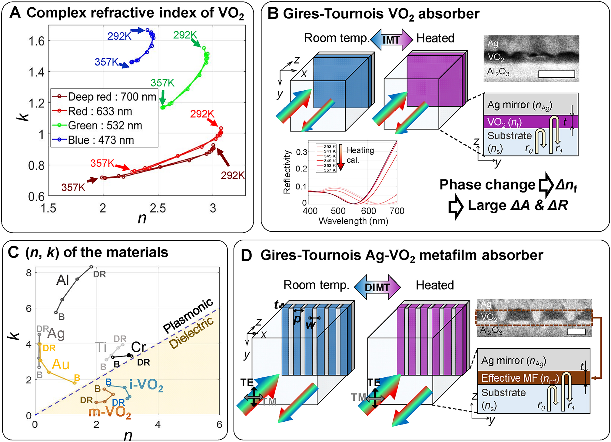
Concept of dynamically tunable phase-change VO2 metafilm absorber.
(A) Measured thermally driven cyclic evolutions of (n, k) coordinates of VO2 at the representative blue (473 nm), green (532 nm), red (633 nm), and deep red (700 nm) colors. (B) Schematic illustration, cross-sectional scanning electron microscopy (SEM) image of the sapphire substrate-VO2-Ag Gires-Tournois absorber (t = 40 nm), and calculated results of tunable near-unity absorption spectra of the absorber during heating. (C) Complex refractive index map for various materials and VO2 at the representative four visible wavelengths (B: blue (473 nm), DR: deep red (700 nm)). (D) Schematic description of phase-change metafilm based dynamic Gires-Tournois absorber. SEM image shows cross-sectional image of the fabricated dynamic Gires-Tournois metafilm absorber with Ag filling factor about 0.2. The scale bars in SEM images of (B) and (D) denote 100 nm.
A baer VO2 film shows low modulation performance owing to theoretically limited maximal absorption of 0.5 [46], [47]. On the other hand, it is well known that a Gires-Tournois VO2 absorber configuration (Figure 1B and Figure S2 of Supplementary Materials) shows large modulation depth (ηm) of light intensity by excitation and modulation of near-unity absorption. Here, ηm is defined as ηm = |Ii−Im|/max(Ii, Im) and Ii and Im correspond to reflection intensities at the insulating and metallic phases, respectively. The two distinct near-unity absorptions in the insulating and metallic phases at the wavelengths of 655 and 550 nm are verified through the theoretical calculation and measurement (Inset reflectance spectra of Figure 1B and Figure S2 of Supplementary Materials). It means the gradual blue and red shifts of absorption dip with change of the resonance wavelength about 100 nm, respectively. Yet, it is still hard to design tunable near-unity absorption with high reflection tunability by only adjusting thickness of VO2 film to meet complex interference conditions of reflection phasors in highly dispersive and absorptive PCM such as VO2 (the Section 3 of the Supplementary Materials).
Here, we introduce a metamaterial-based solution into the Gires-Tournois VO2 absorber scheme to expand range of possible effective refractive index of VO2 film by geometric implanting of subwavelength-spaced periodic nanostructures in an intrinsic PCM VO2, which is called metafilm strategy [48], [49], [50], [51]. We would regard an anisotropic Ag-VO2 film as a tunable effective metafilm with designed effective refractive index and the designed IMT (DIMT). The first step of designing phase-change VO2 metafilm is to choose a proper material to embed geometrically in a VO2 film. Figure 1C describes (n, k) coordinates of the several metals and the two distinct VO2 phases in the visible range. Once a phase-change metafilm is designed as an effective mixture of VO2 and another photonic nanostructure, effective refractive index coordinate of a metafilm would be located at somewhere between the coordinates of the photonic material and that of VO2. Therefore, tunable effective refractive indices at the insulating and metallic phases and thermal transition between those phases could be designed by judicious embedding of certain photonic nanostructures. As shown in Figure 1C, the noble plasmonic metals with less lossy characteristics in the visible range, Al and Ag are the best options to be implanted in VO2 so that the widest range of artificial (n, k) coordinates can be designed and thermally tuned since their (n, k) coordinates are located the most far from the (n, k) coordinates of VO2. We select and embed Ag into the 40 nm-thick VO2 film in the Gires-Tournois VO2 absorber considering both (n, k) design degree of freedom and stable nanofabrication feasibility rather than Al. As a result, PCMA is constructed as depicted in Figure 1D. We demonstrate nanobeam type metafilm in the PCMA configuration with various Ag filling factors, fAg. PCMA depicted in Figure 1D can be approximately modeled as anisotropic effective Gires-Tournois VO2 absorber where dynamic homogeneous permittivity tensor of VO2 layer is artificially designated based on effective medium approximation. This simple concept enlarges the fundamental dynamic dielectric function properties in terms of possible range of spatial encoding as well as polarization-controlled characteristics of it in a single certain device while large dynamic tunability is guaranteed.
For systematic design of VO2 metafilm layer in PCMA configuration, we propose the design rule based on anisotropic counter-intuitive properties of the Wiener’s bounds of effective medium approximation visualized in a complex (n, k) plane [52], [53], [54]. The two bound curves correspond to the normal and parallel effective dielectric functions, εTM and εTE, depending on fAg, respectively. If deep subwavelength resonances around Ag nanobeams are neglected, the ideal analytic first-order approximations of εTM and εTE are harmonic and arithmetic means of constitutive dielectric functions, respectively [52], [53], [54]. In Figure 2A, B, transverse magnetic (TM) and transverse electric (TE) polarization cases are numerically calculated for fAg varying from 0.05 to 0.95 based on complex reflection and transmission coefficients [55], [56].
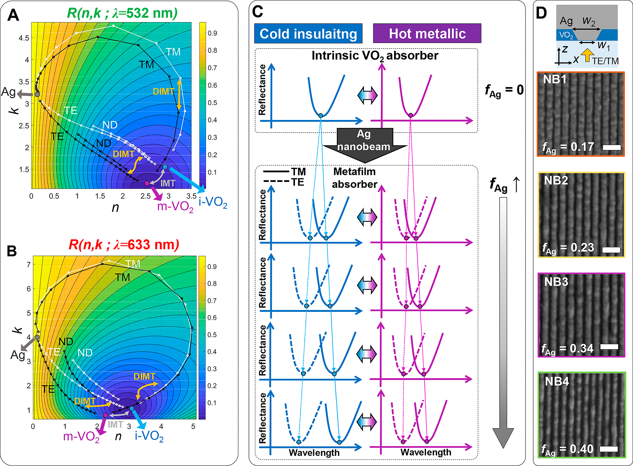
Design principles of anisotropic effective complex refractive indices of VO2 metafilm and designed reflection tunability.
The numerically retrieved Wiener bounds of effective refractive indices with corresponding reflectance maps at the (A) green (532 nm) and (B) red (633 nm) colors. The points marked as Ag, i-VO2, and m-VO2 correspond to (n, k) coordinates of Ag, high index VO2 at the insulating phase, and low index VO2 at the metallic phase at the certain wavelengths, respectively. The white and black dotted lines denote effective refractive index coordinates with VO2 at the insulating and metallic phases, respectively. ND in (A) and (B) implies nanodisk. The ND curves in (A) and (B) imply the VO2 metafilm cases where isotropic circular Ag nanodisks are embedded in the VO2 layer with same fAg (=πr2/p2 where r and p are radius and period of Ag nanodisks) values compared to the Ag nanobeam embedded metafilm absorbers. fAg values of nanobeam and nanodisk type metafilms are varied from 0.05 to 0.95, and from 0.05 to 0.45, respectively. (C) Schematic illustration of intended mechanism and working principle of dynamic Gires-Tornois metafilm absorbers according to periodic photonic doping level of Ag nanobeams. (D) Schematic unitcell description with sidewall tapering effect and top view SEM images of the phase-change metafilm absorbers (PCMAs). Scale bars denote 500 nm.
The effective refractive index retrieval results regarding subwavelength resonant behaviors show similar trend of the zeroth order effective medium approximation (Figure S4 of Supplementary Materials). As fAg increases, effective refractive indices for TM and TE polarizations,
Therefore, it is intuitively expected that the opposite trends of red (for TM) and blue (for TE) shifts of intrinsic absorption dips occur at the both VO2 phases in the same PCMA with certain fAg of Ag nanobeams as described in Figure 2C. In other words, by designed increase and decrease of effective refractive indices of a metafilm layer, both the blue and red shifts of active near-unity absorption can be demonstrated via polarization-controlled operations in a PCMA with certain geometric parameters. The top subfigure of Figure 2D describes the periodic (period of 250 nm) unit cell of PCMA with Ag nanobeams considering tapering effect of ion beam milling fabrication. The four images below the subfigure are top view scanning electron microscopy (SEM) images of the fabricated nanobeam type PCMAs with the four different fAg values (Figure S5 of Supplementary Materials). The fabricated samples would be called as the NB1 (fAg = 0.17), NB2 (fAg = 0.23), NB3 (fAg = 0.34), and NB4 (fAg = 0.40). The corresponding parameter sets of (w1, w2) of the NB1, NB2, NB3, and NB4 are (18 nm, 51 nm), (20 nm, 70 nm), (40 nm, 94 nm), (40 nm, 120 nm), respectively. Here, NB stands for nanobeam. The difference between w1 and w2 accounts for modeling of abovementioned realistic tapering effect in ion beam milling fabrication.
2.2 Underlying physics of tunable phase-change effects using Ag nanobeams
In this section, the physical mechanisms of tunable effective refractive indices and their thermal DIMTs are theoretically studied with respect to effective medium approximation and Fano-like resonance interpretation of the near-unity absorptions. The theoretical concern starts by re-considering validity and assumption of effective medium theory discussed in the previous section. Based on the literature [54], [55], [56] and our numerical data of effective refractive index retrieval (Figure 2A, B and Figure S4 of Supplementary Materials), it is clear that the zeroth order approximation of effective medium approximation is only useful for prediction of anisotropic trend rather than calculation of exact effective refractive index values as the period of nanobeams (250 nm) is not small enough to guarantee the validity of the approximation.
The nanoscale physical origins of such difference between numerically retrieved effective refractive index and the zeroth order analytic effective medium approximation can be explained in terms of plasmonic and Mie-like resonances around Ag nanobeams. In case of TM polarized illumination, Ag nanobeams excite surface plasmons at the both VO2-Ag and Al2O3–Ag interfaces (Figure 3A, B). If fAg is low and widths of nanobeams (w1 and w2) are narrow, near-unity absorption occurs mainly at the Ag-VO2 interface between Ag nanobeams as shown in Figure 3A. However, if fAg, w1, and w2 increases, incident field funneling into the VO2 region between Ag nanobeams gets harder while surface plasmon oscillation at the Al2O3–Ag interface gets easier with the increased interface length and SP excitation efficiency at the boundary of Al2O3–Ag. As refractive index of Al2O3 and effective SP mode index at the Al2O3–Ag interface is smaller than that of VO2 and that at the VO2-Ag interface, resultantly, overall effective resonance area increases by increase of fAg. On the other hand, as TE illumination cannot excite SPs, the dominant region of light trapping and absorbing is the inside of the dielectric VO2 nanobeams capped between the Ag nanobeams via leaky Mie-like TE resonance (Figure 3C, D). As a result, the decreased size of VO2 nanobeams owing to increased fAg induces decrease of effective resonator size and blue shift of resonance. In Figure 4A–H, anisotropic designer shifts and thermal tunings of near-unity absorption dips in the devices are verified numerically (Figure 4A–D) and experimentally (Figure 4E–H). When we compare Figure 4A–D, the red (TM) and blue (TE) shifts of the near-unity absorption dips owing to the opposite changes of the effective refractive indices are numerically verified according to the increase of fAg.
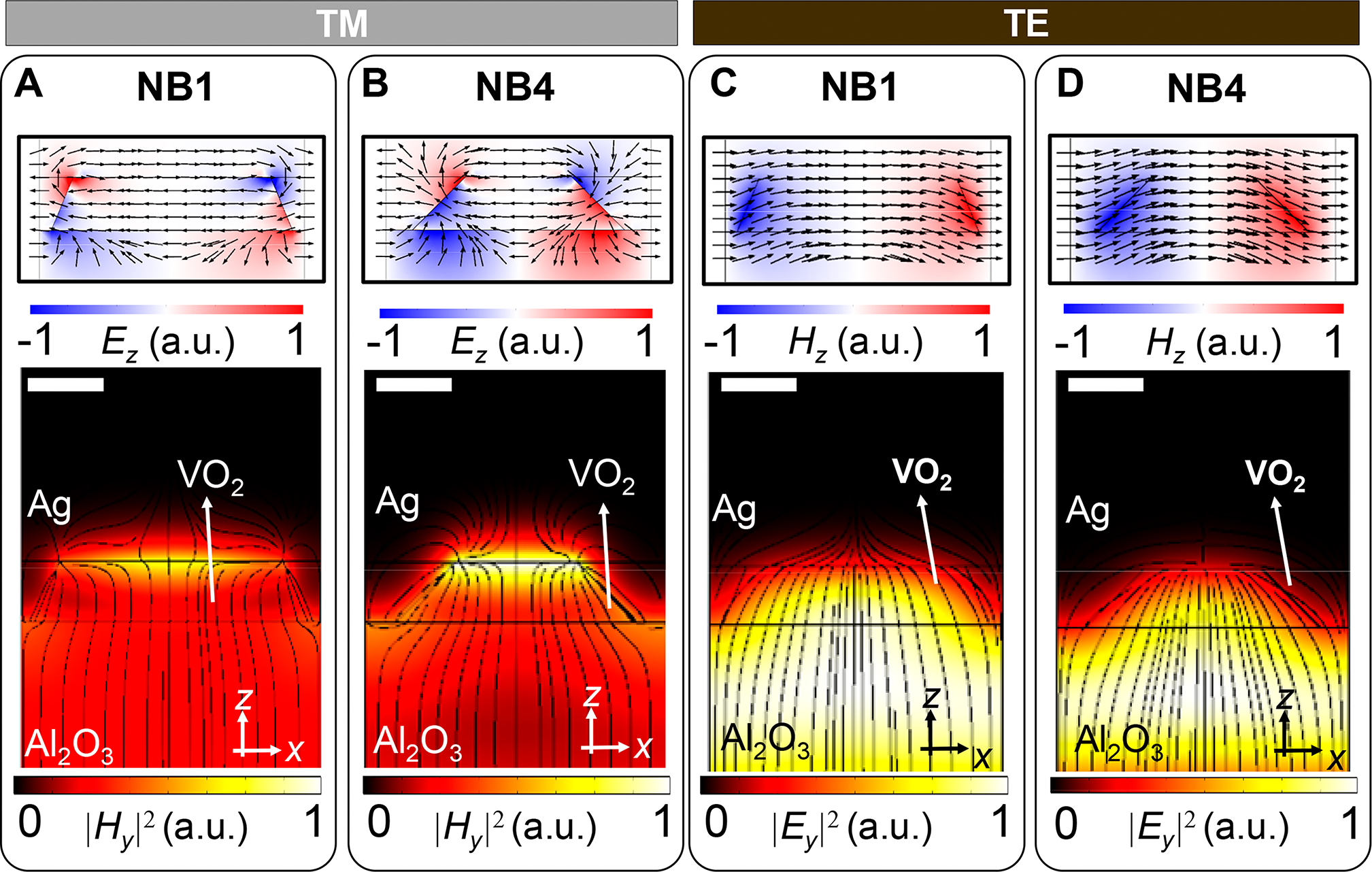
Nanoscopic mechanisms of the resonant near-unity absorptions: subwavelength light funneling into the metafilms.
Electromagnetic field profiles of (A, C) NB1 and (B, D) NB4 devices are numerically investigated at the resonances in the insulating phase for (A, B) TM and (C, D) TE illumination, respectively. Upper figures show the (A, B) Ez and (C, D) Hz, with the normalized black vector arrows of (a, b) displacement current and (c, d) magnetic field, respectively. Lower figures show normalized electromagnetic field profiles of (A, B) |Hy|2 and (C, D) |Ey|2. Black lines in the lower figures depict the flow of Poynting vectors coming from the free space of Al2O3 substrate to the PCMA structures. The scale bars correspond to 60 nm.
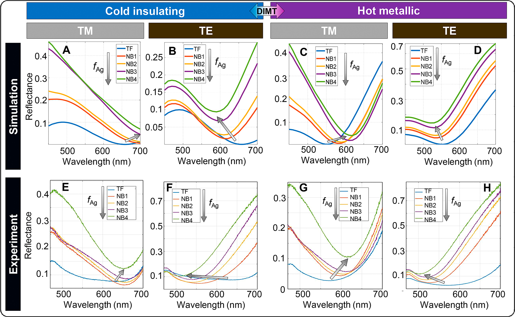
Effects of Ag nanobeams on the dynamic modulation range.
Polarization and temperature dependent reflectance spectra of the PCMAs with varying fAg (0, 0.17, 0.23, 0.34, 0.4) obtained from (A–D) simulations and (E–H) experiments. (A, B, E, F) present polarization dependent spectra at the cold insulating phase of VO2 while (C, D, G, H) present those at the hot metallic phase of VO2. (A, C, E, G) and (B, D, F, H) show reflectance under TM and TE polarized normal illumination cases, respectively. The legend, TF, refers to the case of intrinsic thin film VO2 without Ag embedding (the Gires-Tournois VO2 abosrber case when fAg is zero). The direction of gradually colored arrows in (A-H) imply the increase of fAg.
Moreover, it is noteworthy that large near-unity absorption is achieved even though fAg increases so that large modulation depth is still achieved over the two wavelength bands for a certain PCMA device under the two polarizations (TM and TE). Figure 4E–H successfully verifies the numerical designs of extraordinary modulations via experimental results. We fabricated the micron scale PCMAs via four steps with pulsed laser deposition, e-beam evaporation, and focused ion beam milling. We measured the temperature-dependent backscattering spectra from the PCMA samples (See Experimental sections for the details.).
The fAg-controlled design of reflection spectra in Figure 4 involves the fascinating interference phenomena through the two distinct reflection mechanisms owing to both effective medium approximation and the subwavelength absorption resonances (Figure 3). Here, we introduce Fano-like resonance modeling based on temporal coupled mode theory for quantitative analysis on the two effects to understand the underlying mechanisms of the high-contrast reflection wave modulations. Over the decade, temporal coupled mode theory has been widely utilized to interpret Fano and Fano-like resonances stemming from interference between direct and in-direct scatterings of transmission and reflection waves [57], [58], [59], [60], [61]. In this case, the proposed PCMA can be modeled as a resonator with a single port and a single resonance at the each VO2 phase (Figure 5A). Here, a direct reflection wave can be explained by the Fresnel-Airy reflection formula based on the first order analytic effective medium approximation (Section 6 of Supplementary Materials) and in-direct reflection wave can be modeled as scattering from TM (plasmonic) and TE (Mie-like) resonances discussed above [58], [61].
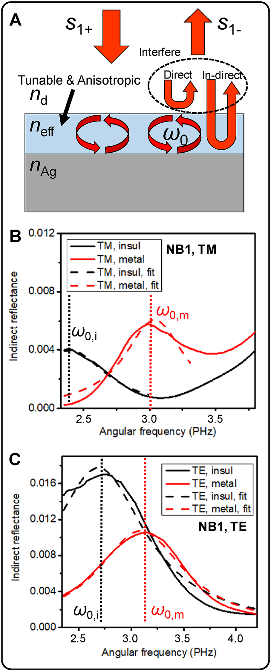
Fano-like resonance modeling.
(A) Schematic illustration of the modeling of the dynamic dual resonances as Fano-like interferences between direct and in-direct reflection waves. (B, C) Indirect reflectance spectra of the NB1 metafilm when fAg is 0.17 neglecting tapering walls and their Lorentzian fitting results. The Indirect reflectance spectra and their fitting results for (B) TM and (C) TE polarizations, respectively. The legends account for polarization direction and phase of VO2. The dashed lines in (B) and (C) are the results of Lorentzian fitting near resonances.
Assuming
Here, D, γ, ω0, and φ are real valued constants and D, γ, and ω0 are positive real values. The fitting to extract proper D, γtot, ω0, and φ is conducted as follows. At first, rid is calculated by subtracting analytic rd based neff from rtot obtained from numerical full field simulation and
2.3 Versatile optical applications and design extensibility
In this section, we prove excellent multiple functionalities of a single PCMA device as dynamic optical applications based on high-contrast gradual phase-change capabilities and polarization-controlled responses. As the NB1 sample with fAg about 0.17 shows the best (high-contrast and largely anisotropic) dynamic performances of near-unity absorptions among the demonstrated NB-type samples, it is considered to investigate gradual thermal modulation of both large anisotropy and near-unity absorptions. Figure 6A, B exhibit gradual blue shifts of resonance in the NB1 sample in cases of TM and TE-polarized illuminations via thermal heating in the different wavelength regions. It implies that the NB1 sample with a fixed geometry can continuously shift a near-unity absorption dip in a broad bandwidth of wavelength ranging from about 530 nm to about 670 nm by help of polarization control. Under TM and TE polarizations, blue shifts of absorption dips are verified from about 670 to 590 nm and from about 570 to 530 nm, respectively. The gradual measurement results of the NB1 sample show good agreement with numerical simulation results both in heating and cooling processes (Figure 3A, B and Section 8 of Supplementary Materials).
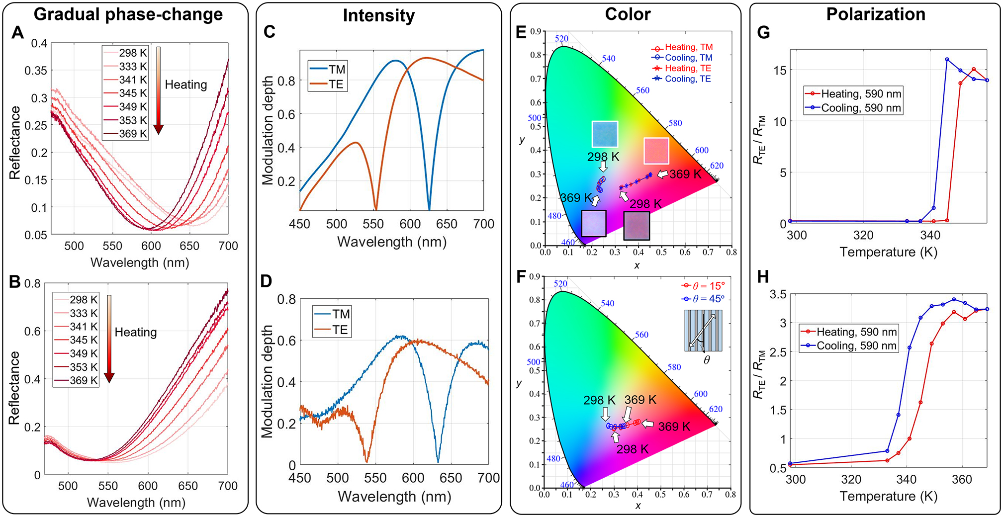
Optical applications of an anisotropic PCMA: modulation of intensity, color, and polarization.
(A, B) Heating induced gradual tuning of near-unity absorption spectra of the NB1 sample under illumination of (A) TM- and (B) TE-polarized light, respectively. Anisotropic broadband modulation depth spectra of reflection intensity from the NB1 sample obtained from (C) full-field simulation and (D) experiment. (E) Polarization-dependent gradual multi-level coloring of the NB1 sample described in CIE space. (F) Polarization rotation controlled intermediate color generations with the NB1 sample between TE and TM curves during the heating processes. The inset figure depicts top view scheme when linearly polarized light normally illuminates the sample with rotation angle, θ. (G, H) Thermally switchable RTE/RTM of the NB1 device, at the wavelength of 590 nm derived from (G) simulation and (H) experiment, respectively.
These largely anisotropic and gradually tunable phase-change characteristics of a single PCMA device can be applied to multiple high-contrast modulations of broadband intensity, reflected color, and polarization direction. Numerical and experimental results of Figure 6C, D shows that intensity of reflected wave is thermally modulated with large modulation depth over broad bandwidths both for TM and TE polarizations. In terms of the locations of modulation depth minimum and maximum, the results of the simulation and measurement show good agreement. However, the maximum value of measured modulation depth (∼0.6) is a bit lower than that of simulation (∼0.9). We guess that a bit larger reflectance of measurement rather than simulation is mainly due to offset baseline reflection from the air-substrate side (seen in measurement configuration in Figure S11) not considered in simulations, and sidewall imperfection of fabrication (seen in Figure S5). In particular, the baseline reflection from air-sapphire substrate for normal illumination is about 0.077 (7.7%) at the wavelength of 600 nm, which is a considerable value when calculating modulation depth.
Moreover, color spectrum and polarization direction of reflected light are also gradually modulated with high contrast in the certain device. Figure 6E shows thermally-driven gradual color generation along largely separated Commission internationale de l’éclairage (CIE) curves according to polarization direction. Blue to light violet and violet to orange thermal colorings are verified experimentally under illumination of TM and TE polarizations, respectively. Here, reflection Jones matrix of a PCMA, r(λ, T), can be written as the Eq. (2).
In this formalism, (1 0)T and (0 1)T correspond to TE and TM polarization Jones vectors while
In case of polarization direction, tunable polarization filtering between nearly-TM and nearly-TE polarizations can be achieved at certain resonant wavelength. In Figure 6A, B, the near-unity absorption dip of the NB1 sample at the insulating phase for TE polarization and that at the metallic phase for TM polarization are closely met (The dip wavelengths are about 610 and 590 nm, respectively. Also see Section 9 of Supplementary Materials.). At the wavelengths near those dip positions, 590 and 610 nm, reflectance is highly anisotropic. Particularly at the wavelength of 590 nm, numerically calculated reflectance ratio defined as RTE/RTM = |rTE/rTM|2 is modulated between about 0 and 14 via heating and cooling (Figure 6G and the Section 8 of Supplementary Materials). As described in Figure 6H, experimental results at the same wavelength exhibit similar trend that reflectance ratio is modulated between about 0.5 and 3.3 in the reconfigurable manner with hysteresis.
As discussed above, it has proved that multi-functional optical applications with the capability of high contrast active thermal modulation are achieved with the PCMAs. Lastly, we would address the design extensibility of the concept for more design degree of freedom in a simple method. Once effective refractive indices of a certain metafilm layer is numerically characterized, this layer can be coupled with other thin film resonators vertically as an example described in Figure 7A. Then, it is possible to calculate reflectance and its tunability only by transfer matrix method without numerical full-field simulations. In case of an example of PCMA heterostructure in Figure 7A, it can exhibit not only near-unity absorptions but also resonant reflection peaks mainly stemming from a Si3N4 etalon. As the transparent dielectric film can induce reflection peaks of Fabry-Pérot resonance (See field profiles in sub-figures of Figure 7B, C), a change of VO2 phase can induce change of coupling between reflective Fabry-Pérot resonance and thermally shifted absorption dip of PCMA. Thus, as shown in Figure 7B, C, thermally-driven blue shifts of absorption dips induce weakened Fabry-Pérot resonance strengths with polarization-dependent manners. Variation of tf would enable shift of a spectral location of a Fabry–Pérot peak and more diverse spectral tunability in the visible spectrum, potentially. In the perspective of dynamic color generation, this novel and simple strategy can dynamically enhance and tune purities of reflection color (Figure 7D) without significant fabrication problems compared to the original PCMA devices. Such PCMA heterostructures also hold a potential of vertical integration with other functional metasurfaces [62], [63], [64].
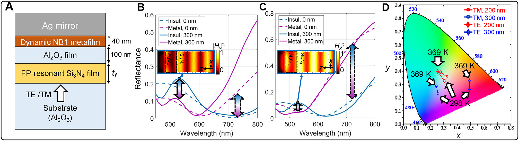
Dynamic metafilm heterostructure absorber: extensibility of the phase-change metafilm for extraordinary spectrum tunability.
(A) Schematic illustration of of Si3N4 film inserted PCMA heterostructure using the NB1 metafilm. Phase-change tunability of device described under (B) TM and (C) TE illuminations, respectively. Sub-figures of (B, C) present spatial intensity profiles of Hy and Hx fields at the reflection peaks at the insulating phase, respectively. The legends in (B, C) describe phase of VO2 and value of tf. (D) Reflected anisotropic color tunability of the device described in (A) is graphically shown in CIE space. The legends imply polarization and values of tf (200 and 300 nm).
3 Conclusion
Inspired by near-unity absorption in ultrathin Gires-Tournois absorber and effective medium approximation, we have shown the simple and powerful framework, PCMA, for effective and versatile modulations of visible light with a single chip in a reconfigurable manner. We expect that the proposed concept would be fruitful for improvement of various integrated optoelectronics technologies for compact spatial light modulator, photodetector, compact reflective display, and multiplexed image sensors that essentially require compact and dynamic visible range operation. Moreover, it seems to be promising that the proposed strategy based on noble metal-embedding could be a milestone research for sub-micron active modulator pixels, if pixel-by-pixel electro-thermal control is achieved in the future, which is one of the ultimate goals of dynamic nanophotonics.
4 Experimental section
4.1 Sample fabrication
The device was fabricated through the four steps. Firstly, we use a pulsed laser deposition method (LAMBDA PHYSIK, COMPEX 205) with a KrF excimer laser at 248 nm for deposition of 40 nm-thick VO2 on a sapphire substrate. Secondly, 150 nm-thick Ag was deposited for a hard mask on a VO2 film by e-beam evaporation (Korea Vacuum Tech, KVE-3004). Then, 10 μm by 10 μm sized nanobeam-type patterns were defined by focused ion beam milling machine (FEI, Quanta 200 3D). Ag hard mask enables accurate high resolution focused ion beam patterning in large area and protects VO2 film from direct stoichiometric Ga+ ion contamination which would deteriorate molecular bonding structure as defects [23]. At last, we deposited a 200 nm-thick Ag film by e-beam evaporation to form metallic inclusions and mirrors.
4.2 Material property measurement
Temperature-dependent cyclic evolution of dielectric functions of 40 nm-thick VO2 film is measured by using a variable angle spectroscopic ellipsometer system (J. A. Woollam, V-VASE) and temperature-controlled Peltier stage (Linkam, PE120). The complex refractive indices and effective exact thickness of VO2 film have been fitted by Kramers-Kroning relation and general oscillator model with combination of Tauc-Lorentz, Lorentz, and Drude oscillators (Section 10 of Supplementary Materials). We used the measured permittivity data of metals and Al2O3 measured by E. D. Palik [65] and I. H. Malitson [66]. Temperature-dependent resistivity of a VO2 film is measured for the verification of IMT phenomena using a source meter, a hot plate, and a thermocouple (Figure S12 of Supplementary Materials). Atomic force micrograph (Park Systems, XE150) is scanned with non-contact type tip for surface roughness and grain measurement of VO2 film (Figure S10 of Supplementary Materials).
4.3 Temperature-controlled bright field backscattering spectroscopy and imaging
Bright field backscattering spectra from microscopic metafilm samples are measured using our custom-built setup with an optical microscope and spectrometer (Princeton Instruments, SpectraPro 2300) (Figure S11 of Supplementary Materials). Temperature of the samples were controlled by Peltier stage (Linkam, PE120) in our thermostatic laboratory of about 20 °C. Spectral data is scanned over about 6 μm by 6 μm region of samples through an aperture of spectrometer. Broadband illumination of white light (Thorlabs, MNWHL4 LED) is focused on the sample through the iris, broadband polarizer, and 50X objective lens. The spectra are normalized by the reflection spectrum from a sapphire substrate coated by optically thick silver film (deposited with the thickness over 500 nm by e-beam evaporation). The 100X magnified charge coupled device images are captured under the incidence of our neutral white light emitting diode.
4.4 Numerical simulation
Electromagnetic full field simulations are conducted with commercial finite element method tool (COMSOL Multiphysics 5.3, RF module, Frequency domain solver).
Funding source: National Research Foundation of Korea
Funding source: MSIT
Award Identifier / Grant number: 2020R1A2B5B02002730
Acknowledgments
This work was supported by the National Research Foundation of Korea (NRF) grant funded by the Korea government (MSIT) (No. 2020R1A2B5B02002730). We deeply thank Dr. So Yeun Kim of IBS Center for Correlated Electron Systems for their help of the VO2 ellipsometry measurement. We also thank to Dr. Joonsoo Kim for fruitful discussions about theoretical analysis. Part of this study has been performed using facilities at IBS Center for Correlated Electron Systems of Seoul National University, Electronics and Telecommunications Research Institute, and National Center for Inter-University Research Facilities of Seoul National University.
Author contribution: S.-J. K. conceived the idea, conducted material investigation, analytical modeling, numerical design, fabrication and measurement of the devices, and preparation of the draft. H. Y., J.-G. Y., and S.-Y. L. helped measurement and data analysis. Y. L., J. S., and C. C. helped measurement. S. C., K. P., S. J. J., and Y. W. L. deposited vanadium dioxide thin films. J. H. helped theoretical discussions. B. L. initiated and supervised the project. All of the authors participated in discussions and approved the submission of the manuscript.
Research funding: None declared.
Conflict of interest statement: The authors declare no conflict of interest.
References
[1] M. Ferrera, N. Kinsey, A. Shaltout, C. DeVault, V. Shalaev, and A. Boltasseva, “Dynamic nanophotonics,” J. Opt. Soc. Am. B, vol. 34, no. 1, pp. 95–103, 2017, https://doi.org/10.1364/josab.34.000095.10.1364/JOSAB.34.000095Search in Google Scholar
[2] S. V. Makarov, A. S. Zalogina, M. Tajik, et al., “Light‐induced tuning and reconfiguration of nanophotonic structures,” Laser Photon. Rev., vol. 11, no. 5, p. 1700108, 2017, https://doi.org/10.1002/lpor.201700108.Search in Google Scholar
[3] N. I. Zheludev and Y. Kivshar, “From metamaterials to metadevices. Nat. Mater., vol. 11, no. 11, pp. 917–924, 2012, https://doi.org/10.1038/nmat3431.Search in Google Scholar
[4] S. M. Choudhury, D. Wang, K. Chaudhuri, et al., “Material platforms for optical metasurfaces,” Nanophotonics, vol. 7, no. 6, pp. 959–987, 2018, https://doi.org/10.1515/nanoph-2017-0130.Search in Google Scholar
[5] M. Wuttig, H. Bhaskaran, and T. Taubner, “Phase-change materials for non-volatile photonic applications,” Nat. Photon., vol. 11, no. 8, p. 465, 2017, https://doi.org/10.1038/nphoton.2017.126.Search in Google Scholar
[6] N. R. Hosseini and J. Rho, “Metasurfaces based on phase-change material as a reconfigurable platform for multifunctional devices,” Materials, vol. 10, no. 9, p. 1046, 2017, https://doi.org/10.3390/ma10091046.Search in Google Scholar
[7] D. M. Wu, M. L. Solomon, G. V. Naik, et al., “Chemically responsive elastomers exhibiting unity‐order refractive index modulation,” Adv. Mater., vol. 30, no. 7, p. 1703912, 2018, https://doi.org/10.1002/adma.201703912.Search in Google Scholar
[8] J. Y. Kim, H. Kim, B. H. Kim, et al., “Highly tunable refractive index visible-light metasurface from block copolymer self-assembly,” Nat. Commun., vol. 7, no. 1, pp. 1–9, 2016, https://doi.org/10.1038/ncomms12911.Search in Google Scholar
[9] M. S. Jang, V. W. Brar, M. C. Sherrott, et al., “Tunable large resonant absorption in a midinfrared graphene Salisbury screen,” Phys. Rev. B, vol. 90, no. 16, p. 165409, 2014, https://doi.org/10.1103/physrevb.90.165409.Search in Google Scholar
[10] V. E. Babicheva, A. Boltasseva, and V. Lavrinenko, “Transparent conducting oxides for electro-optical plasmonic modulators,” Nanophotonics, vol. 1, pp. 165–185, 2015, https://doi.org/10.1515/nanoph-2015-0004.Search in Google Scholar
[11] A. Howes, W. Wang, I. Kravchenko, and J. Valentine, “Dynamic transmission control based on all-dielectric Huygens metasurfaces,” Optica, vol. 5, no. 7, pp. 787–792, 2018, https://doi.org/10.1364/optica.5.000787.Search in Google Scholar
[12] J. Park and S. J. Kim, “Subwavelength-spaced transmissive metallic slits for 360-degree phase control by using transparent conducting oxides,” Appl. Opt., vol. 57, no. 21, pp. 6027–6031, 2018, https://doi.org/10.1364/ao.57.006027.Search in Google Scholar
[13] G. K. Shirmanesh, R. Sokhoyan, R. A. Pala, and H. A. Atwater, “Dual-gated active metasurface at 1550 nm with wide (> 300°) phase tunability,” Nano Lett., vol. 18, no. 5, pp. 2957–2963, 2018, https://doi.org/10.1021/acs.nanolett.8b00351.Search in Google Scholar
[14] E. Li, Q. Gao, R. T. Chen, and A. X. Wang, “Ultracompact silicon-conductive oxide nanocavity modulator with 0.02 lambda-cubic active volume,” Nano Lett., vol. 18, no. 2, pp. 1075–1081, 2018, https://doi.org/10.1021/acs.nanolett.7b04588.Search in Google Scholar
[15] Y. Horie, A. Arbabi, E. Arbabi, S. M. Kamali, and A. Faraon, “High-speed, phase-dominant spatial light modulation with silicon-based active resonant antennas,” ACS Photon., vol. 5, no. 5, pp. 1711–1717, 2017, https://doi.org/10.1021/acsphotonics.7b01073.Search in Google Scholar
[16] R. Bruck, K. Vynck, P. Lalanne, et al., “All-optical spatial light modulator for reconfigurable silicon photonic circuits,” Optica, vol. 3, no. 4, pp. 396–402, 2016, https://doi.org/10.1364/optica.3.000396.Search in Google Scholar
[17] T. Driscoll, H. T. Kim, B. G. Chae, et al., “Memory metamaterials,” Science, vol. 325, no. 5947, pp. 1518–1521, 2009, https://doi.org/10.1126/science.1176580.Search in Google Scholar
[18] M. J. Dicken, K. Aydin, I. M. Pryce, et al., “Frequency tunable near-infrared metamaterials based on VO2 phase transition,” Opt. Express, vol. 17, no. 20, pp. 18330–18339, 2009, https://doi.org/10.1364/oe.17.018330.Search in Google Scholar
[19] S. J. Kim, H. Yun, K. Park, et al., “Active directional switching of surface plasmon polaritons using a phase transition material,” Sci. Rep., vol. 7, p. 43723, 2017, https://doi.org/10.1038/srep43723.Search in Google Scholar
[20] S. J. Kim, S. Choi, C. Choi, et al., “Broadband efficient modulation of light transmission with high contrast using reconfigurable VO2 diffraction grating,” Opt. Express, vol. 26, no. 26, pp. 34641–34654, 2018, https://doi.org/10.1364/oe.26.034641.Search in Google Scholar
[21] M. Seo, J. Kyoung, H. Park, et al., “Active terahertz nanoantennas based on VO2 phase transition,” Nano Lett., vol. 10, no. 6, pp. 2064–2068, 2010, https://doi.org/10.1021/nl1002153.Search in Google Scholar
[22] M. A. Kats, R. Blanchard, S. Zhang, et al., “Vanadium dioxide as a natural disordered metamaterial: perfect thermal emission and large broadband negative differential thermal emittance,” Phys. Rev. X, vol. 3, no. 4, p. 041004, 2013, https://doi.org/10.1103/physrevx.3.041004.Search in Google Scholar
[23] J. Rensberg, S. Zhang, Y. Zhou, et al., “Active optical metasurfaces based on defect-engineered phase-transition materials,” Nano Lett., vol. 16, no. 2, p. 1050, 2016, https://doi.org/10.1021/acs.nanolett.5b04122.Search in Google Scholar
[24] M. A. Kats, D. Sharma, J. Lin, et al., “Ultra-thin perfect absorber employing a tunable phase change material,” Appl. Phys. Lett., vol. 101, no. 22, p. 1050, 2012, https://doi.org/10.1063/1.4767646.Search in Google Scholar
[25] T. Driscoll, S. Palit, M. M. Qazilbash, et al., “Dynamic tuning of an infrared hybrid-metamaterial resonance using vanadium dioxide,” Appl. Phys. Lett., vol. 93, no. 2, p. 024101, 2008, https://doi.org/10.1063/1.2956675.Search in Google Scholar
[26] Z. Zhu, P. G. Evans, R. F. HaglundJr, and J. G. Valentine, “Dynamically reconfigurable metadevice employing nanostructured phase-change materials,” Nano Lett., vol. 17, no. 8, pp. 4881–4885, 2017, https://doi.org/10.1021/acs.nanolett.7b01767.Search in Google Scholar
[27] Y. Ke, X. Wen, D. Zhao, R. Che, Q. Xiong, and Y. Long, “Controllable fabrication of two-dimensional patterned VO2 nanoparticle, nanodome, and nanonet arrays with tunable temperature-dependent localized surface plasmon resonance,” ACS Nano, vol. 11, no. 7, pp. 7542–7551, 2017, https://doi.org/10.1021/acsnano.7b02232.Search in Google Scholar
[28] N. A. Butakov, I. Valmianski, T. Lewi, et al., “Switchable plasmonic–dielectric resonators with metal–insulator transitions,” ACS Photon., vol. 5, no. 2, pp. 371–377, 2018, https://doi.org/10.1021/acsphotonics.7b00334.Search in Google Scholar
[29] Z. Xu, Q. Li, K. K. Du, et al., “Spatially resolved dynamically reconfigurable multilevel control of thermal emission,” Laser Photon. Rev., vol. 14, no. 1, p. 1900162, 2020, https://doi.org/10.1002/lpor.201900162.Search in Google Scholar
[30] B. Gholipour, J. Zhang, K. F. MacDonald, D. W. Hewak, and N. I. Zheludev, “An all‐optical, non‐volatile, bidirectional, phase‐change meta‐switch,” Adv. Mater., vol. 25, no. 22, pp. 3050-4, 2013, https://doi.org/10.1002/adma.201300588.Search in Google Scholar
[31] Q. Wang, E. T. Rogers, B. Gholipour, et al., “Optically reconfigurable metasurfaces and photonic devices based on phase change materials,” Nat. Photon., vol. 10, no. 1, p. 60, 2016, https://doi.org/10.1038/nphoton.2015.247.Search in Google Scholar
[32] A. Karvounis, B. Gholipour, K. F. MacDonald, and N. I. Zheludev, “All-dielectric phase-change reconfigurable metasurface,” Appl. Phys. Lett., vol. 109, no. 5, p. 051103, 2016, https://doi.org/10.1063/1.4959272.Search in Google Scholar
[33] X. Yin, T. Steinle, L. Huang, et al., “Beam switching and bifocal zoom lensing using active plasmonic metasurfaces,” Light Sci. Appl., vol. 6, no. 7, p. e17016, 2017, https://doi.org/10.1038/lsa.2017.16.Search in Google Scholar
[34] C. Choi, S. Y. Lee, S. E. Mun, et al., “Metasurface with nanostructured Ge2Sb2Te5 as a platform for broadband‐operating wavefront switch,” Adv. Opt. Mater., vol. 7, no. 12, p. 1900171, 2019, https://doi.org/10.1002/adom.201900171.Search in Google Scholar
[35] C. Y. Hwang, G. H. Kim, J. H. Yang, et al., “Rewritable full-color computer-generated holograms based on color-selective diffractive optical components including phase-change materials,” Nanoscale, vol. 10, no. 46, pp. 21648–21655, 2018, https://doi.org/10.1039/c8nr04471f.Search in Google Scholar
[36] B. Gholipour, A. Karvounis, J. Yin, C. Soci, K. F. MacDonald, and N. I. Zheludev, “Phase-change-driven dielectric-plasmonic transitions in chalcogenide metasurfaces,” NPG Asia Mater., vol. 10, no. 6, pp. 533–539, 2018, https://doi.org/10.1038/s41427-018-0043-4.Search in Google Scholar
[37] P. Hosseini, C. D. Wright, and H. Bhaskaran, “An optoelectronic framework enabled by low-dimensional phase-change films,” Nature, vol. 511, no. 7508, pp. 206–211, 2014, https://doi.org/10.1038/nature13487.Search in Google Scholar
[38] S. Y. Lee, Y. H. Kim, S. M. Cho, et al., “Holographic image generation with a thin-film resonance caused by chalcogenide phase-change material,” Sci. Rep., vol. 7, no. 1, p. 41152, 2017, https://doi.org/10.1038/srep41152.Search in Google Scholar
[39] A. Tittl, A. K. U. Michel, M. Schäferling, et al., “A switchable mid‐infrared plasmonic perfect absorber with multispectral thermal imaging capability,” Adv. Mater., vol. 27, no. 31, pp. 4597–4603, 2015, https://doi.org/10.1002/adma.201502023.Search in Google Scholar
[40] K. K. Du, Q. Li, Y. B. Lyu, et al., “Control over emissivity of zero-static-power thermal emitters based on phase-changing material GST,” Light Sci. Appl., vol. 6, no. 1, p. e16194, 2017, https://doi.org/10.1038/lsa.2016.194.Search in Google Scholar
[41] Y. Qu, Q. Li, L. Cai, et al., “Thermal camouflage based on the phase-changing material GST,” Light Sci. Appl., vol. 7, no. 1, p. 1, 2018, https://doi.org/10.1038/s41377-018-0038-5.Search in Google Scholar
[42] Z. Li, Y. Zhou, H. Qi, et al., “Correlated perovskites as a new platform for super‐broadband‐tunable photonics,” Adv. Mater., vol. 28, no. 41, pp. 9117–9125, 2016, https://doi.org/10.1002/adma.201601204.Search in Google Scholar
[43] M. A. Kats, R. Blanchard, P. Genevet, and F. Capasso, “Nanometre optical coatings based on strong interference effects in highly absorbing media,” Nat. Mater., vol. 12, no. 1, pp. 20–24, 2013, https://doi.org/10.1038/nmat3443.Search in Google Scholar
[44] J. Park, S. J. Kim, and M. L. Brongersma, “Condition for unity absorption in an ultrathin and highly lossy film in a Gires–Tournois interferometer configuration,” Opt. Lett., vol. 40, no. 9, pp. 1960–1963, 2015, https://doi.org/10.1364/ol.40.001960.Search in Google Scholar
[45] M. M. Qazilbash, A. A. Schafgans, K. S. Burch, et al., “Electrodynamics of the vanadium oxides VO2 and V2O3,” Phys. Rev. B, vol. 77, no. 11, p. 115121, 2008, https://doi.org/10.1103/physrevb.77.115121.Search in Google Scholar
[46] W. W. Salisbury. “Absorbent body for electromagnetic waves,” U.S. 2,599,944, 1952.Search in Google Scholar
[47] R. L. Fante and M. T. Mccormack, “Reflection properties of the Salisbury screen,” IEEE Trans. Antennas Propag., vol. 36, no. 10, pp. 1443–1454, 1988, https://doi.org/10.1109/8.8632.Search in Google Scholar
[48] I. Liberal, A. M. Mahmoud, Y. Li, B. Edwards, and N. Engheta, “Photonic doping of epsilon-near-zero media,” Science, vol. 355, no. 6329, pp. 1058–1062, 2017, https://doi.org/10.1126/science.aal2672.Search in Google Scholar
[49] S. J. Kim, P. Fan, J. H. Kang, and M. L. Brongersma, “Creating semiconductor metafilms with designer absorption spectra,” Nat. Commun., vol. 6, no. 1, pp. 1–8, 2015, https://doi.org/10.1038/ncomms8591.Search in Google Scholar
[50] S. J. Kim, J. Park, M. Esfandyarpour, E. F. Pecora, P. G. Kik, and M. L. Brongersma, “Superabsorbing, artificial metal films constructed from semiconductor nanoantennas,” Nano Lett., vol. 16, no. 6, pp. 3801–3808, 2016, https://doi.org/10.1021/acs.nanolett.6b01198.Search in Google Scholar
[51] M. Esfandyarpour, E. C. Garnett, Y. Cui, M. D. McGehee, and M. L. Brongersma, “Metamaterial mirrors in optoelectronic devices,” Nat. Nanotechnol., vol. 9, no. 7, p. 542, 2014, https://doi.org/10.1038/nnano.2014.117.Search in Google Scholar
[52] O. Wiener. “Die Theorie des Mischkorpers fur das Feld der stationaren Stromung.” Abh Math-Phys Klasse Koniglich Sachsischen Des Wiss, vol. 32, pp. 507–604, 1912.Search in Google Scholar
[53] W. Cai and V. Shalaev, Optical metamaterials: fundamentals and applications, New York, NY, Springer Science & Business Media, 2009.Search in Google Scholar
[54] P. Lalanne and J. P. Hugonin, “High-order effective-medium theory of subwavelength gratings in classical mounting: application to volume holograms,” J. Opt. Soc. Am. A, vol. 15, no. 7, pp. 1843–1851, 1998, https://doi.org/10.1364/josaa.15.001843.Search in Google Scholar
[55] A. Fang, T. Koschny, and C. M. Soukoulis, “Optical anisotropic metamaterials: negative refraction and focusing,” Phys. Rev. B, vol. 79, no. 24, p. 245127, 2009, https://doi.org/10.1103/physrevb.79.245127.Search in Google Scholar
[56] D. R. Smith, D. C. Vier, T. Koschny, and C. M. Soukoulis, “Electromagnetic parameter retrieval from inhomogeneous metamaterials,” Phys. Rev. E, vol. 71, no. 13, p. 036617, 2005, https://doi.org/10.1103/physreve.71.036617.Search in Google Scholar
[57] H. A. Haus, Waves and fields in optoelectronics, New Jersey, United States, Prentice-Hall, 1984.Search in Google Scholar
[58] S. Fan, W. Suh, and J. D. Joannopoulos, “Temporal coupled-mode theory for the Fano resonance in optical resonators,” J. Opt. Soc. Am. A, vol. 20, no. 3, pp. 569–572, 2003, https://doi.org/10.1364/josaa.20.000569.Search in Google Scholar
[59] K. X. Wang, Z. Yu, S. Sandhu, and S. Fan, “Fundamental bounds on decay rates in asymmetric single-mode optical resonators,” Opt. Lett., vol. 38, no. 2, pp. 100–102, 2013, https://doi.org/10.1364/ol.38.000100.Search in Google Scholar
[60] J. W. Yoon and R. Magnusson, “Fano resonance formula for lossy two-port systems,” Opt. Exp., vol. 21, no. 15, pp. 17751–17759, 2013, https://doi.org/10.1364/oe.21.017751.Search in Google Scholar
[61] A. Cordaro, J. Van de Groep, S. Raza, E. F. Pecora, F. Priolo, and M. L. Brongersma, “Antireflection high-index metasurfaces combining Mie and Fabry-Pérot resonances,” ACS Photon., vol. 6, no. 2, pp. 453–459, 2019, https://doi.org/10.1021/acsphotonics.8b01406.Search in Google Scholar
[62] J. Van de Groep and M. L. Brongersma, “Metasurface mirrors for external control of Mie resonances,” Nano Lett., vol. 18, no. 6, pp. 3857–3864, 2018, https://doi.org/10.1021/acs.nanolett.8b01148.Search in Google Scholar
[63] J. G. Yun, J. Sung, S. J. Kim, H. Yun, C. Choi, and B. Lee, “Ultracompact meta-pixels for high colour depth generation using a bi-layered hybrid metasurface,” Sci. Rep., vol. 9, no. 1, pp. 1–9, 2019, https://doi.org/10.1038/s41598-019-51946-8.Search in Google Scholar
[64] Y. Zhou, I. I. Kravchenko, H. Wang, H. Zheng, G. Gu, and J. Valentine, “Multifunctional metaoptics based on bilayer metasurfaces,” Light Sci. Appl., vol. 8, no. 1, pp. 1–9, 2019, https://doi.org/10.1038/s41377-019-0193-3.Search in Google Scholar
[65] E. D. Palik, Handbook of Optical Constants of Solids, Orlando, Academic Press, 1985.Search in Google Scholar
[66] I. H Malitson and M. J. Dodge, “Refractive Index and Birefringence of Synthetic Sapphire,” J. Opt. Soc. Am., vol. 62, no. 1405, pp. 11797–2999, 1972.Search in Google Scholar
Supplementary material
The online version of this article offers supplementary material https://doi.org/10.1515/nanoph-2020-0264.
© 2020 Sun-Je Kim et al., published by De Gruyter, Berlin/Boston
This work is licensed under the Creative Commons Attribution 4.0 International License.
Articles in the same Issue
- Editorial
- Editorial
- Optoelectronics and Integrated Photonics
- Disorder effects in nitride semiconductors: impact on fundamental and device properties
- Ultralow threshold blue quantum dot lasers: what’s the true recipe for success?
- Waiting for Act 2: what lies beyond organic light-emitting diode (OLED) displays for organic electronics?
- Waveguide combiners for mixed reality headsets: a nanophotonics design perspective
- On-chip broadband nonreciprocal light storage
- High-Q nanophotonics: sculpting wavefronts with slow light
- Thermoelectric graphene photodetectors with sub-nanosecond response times at terahertz frequencies
- High-performance integrated graphene electro-optic modulator at cryogenic temperature
- Asymmetric photoelectric effect: Auger-assisted hot hole photocurrents in transition metal dichalcogenides
- Seeing the light in energy use
- Lasers, Active optical devices and Spectroscopy
- A high-repetition rate attosecond light source for time-resolved coincidence spectroscopy
- Fast laser speckle suppression with an intracavity diffuser
- Active optics with silk
- Nanolaser arrays: toward application-driven dense integration
- Two-dimensional spectroscopy on a THz quantum cascade structure
- Homogeneous quantum cascade lasers operating as terahertz frequency combs over their entire operational regime
- Toward new frontiers for terahertz quantum cascade laser frequency combs
- Soliton dynamics of ring quantum cascade lasers with injected signal
- Fiber Optics and Optical Communications
- Propagation stability in optical fibers: role of path memory and angular momentum
- Perspective on using multiple orbital-angular-momentum beams for enhanced capacity in free-space optical communication links
- Biomedical Photonics
- A fiber optic–nanophotonic approach to the detection of antibodies and viral particles of COVID-19
- Plasmonic control of drug release efficiency in agarose gel loaded with gold nanoparticle assemblies
- Metasurfaces for biomedical applications: imaging and sensing from a nanophotonics perspective
- Hyperbolic dispersion metasurfaces for molecular biosensing
- Fundamentals of Optics
- A Tutorial on the Classical Theories of Electromagnetic Scattering and Diffraction
- Reflectionless excitation of arbitrary photonic structures: a general theory
- Optimization Methods
- Multiobjective and categorical global optimization of photonic structures based on ResNet generative neural networks
- Machine learning–assisted global optimization of photonic devices
- Artificial neural networks for inverse design of resonant nanophotonic components with oscillatory loss landscapes
- Adjoint-optimized nanoscale light extractor for nitrogen-vacancy centers in diamond
- Topological Photonics
- Non-Hermitian and topological photonics: optics at an exceptional point
- Topological photonics: Where do we go from here?
- Topological nanophotonics for photoluminescence control
- Anomalous Anderson localization behavior in gain-loss balanced non-Hermitian systems
- Quantum computing, Quantum Optics, and QED
- Quantum computing and simulation
- NIST-certified secure key generation via deep learning of physical unclonable functions in silica aerogels
- Thomas–Reiche–Kuhn (TRK) sum rule for interacting photons
- Macroscopic QED for quantum nanophotonics: emitter-centered modes as a minimal basis for multiemitter problems
- Generation and dynamics of entangled fermion–photon–phonon states in nanocavities
- Polaritonic Tamm states induced by cavity photons
- Recent progress in engineering the Casimir effect – applications to nanophotonics, nanomechanics, and chemistry
- Enhancement of rotational vacuum friction by surface photon tunneling
- Plasmonics and Polaritonics
- Shrinking the surface plasmon
- Polariton panorama
- Scattering of a single plasmon polariton by multiple atoms for in-plane control of light
- A metasurface-based diamond frequency converter using plasmonic nanogap resonators
- Selective excitation of individual nanoantennas by pure spectral phase control in the ultrafast coherent regime
- Semiconductor quantum plasmons for high frequency thermal emission
- Origin of dispersive line shapes in plasmon-enhanced stimulated Raman scattering microscopy
- Epitaxial aluminum plasmonics covering full visible spectrum
- Metaoptics
- Metamaterials with high degrees of freedom: space, time, and more
- The road to atomically thin metasurface optics
- Active nonlocal metasurfaces
- Giant midinfrared nonlinearity based on multiple quantum well polaritonic metasurfaces
- Near-field plates and the near zone of metasurfaces
- High-efficiency metadevices for bifunctional generations of vectorial optical fields
- Printing polarization and phase at the optical diffraction limit: near- and far-field optical encryption
- Optical response of jammed rectangular nanostructures
- Dynamic phase-change metafilm absorber for strong designer modulation of visible light
- Arbitrary polarization conversion for pure vortex generation with a single metasurface
- Enhanced harmonic generation in gases using an all-dielectric metasurface
- Monolithic metasurface spatial differentiator enabled by asymmetric photonic spin-orbit interactions