Classification of quantum-spin-hall topological phase in 2D photonic continuous media using electromagnetic parameters
-
Xin-Tao He


Abstract
Refractive index is a fundamental electromagnetic (EM) parameter that can describe photonic continuous media (PCM) traditionally as either transparency or opacity. Recently, topological theory offers a new set of phases to characterize PCM as either trivial or nontrivial, by using topological invariant which are not direct to EM parameters. As all of the optical properties in PCM should be related to EM parameters, we formulate a topological index based on EM parameters and establish its phase map in this work. The map can analytically describe the deterministic condition for a topologically nontrivial phase. Our findings indicate that the topology of 2D bi-anisotropic PCM is determined by the sign of the topological index. Another EM parameter of pseudo surface impedance is also introduced for the opaque regions of PCM, showing the topological opacity has a full range of impedance values ranging from negative to positive, while the trivial case only has either negative or positive impedance. The simulation results show that an interface between two opacities with differing index signs can support robustly optical propagation of topological edge states. The proposal of EM-parameter method reveals a deep understanding on topological properties of PCM, and will enrich the topological theory in photonic systems.
1 Introduction
Topology, a concept originating from mathematics, has attracted widespread attention in the physics world, from condensed matter to classical waves [1], [2]. The rapid developments in topological photonics [3], [4], [5], [6], [7] have created an advanced platform at both microwave and optical frequencies for flexibly controlling various types of topological phases, such as quantum anomalous/spin/valley Hall effects [8], [9], [10], [11], [12], [13], [14], [15], [16], [17], [18], [19], [20], [21] and 1D/2D Zak phases [22], [23], [24], [25], [26], [27], [28], [29], [30], [31]. Furthermore, topological photonics give a new paradigm to design on-chip devices, especially promising for nanophotonics and integrated optics [15], [32], [33], [34], [35]. These intriguing features in principle are derived from the topological band theory, which can theoretically predict nontrivial evolution of band structures and protections of topological states in the k space [36]. For photonic systems, a general method to mimic the effective model of topological band theory is the exploration of photonic periodic lattice (PPL). As one of the common cases, photonic crystals support Bloch waves in its building blocks [7], [37], and some of the eigenmodes around high-symmetry k points can be approximately described by the effective Hamiltonian. Based on the band-eigenfield method, one can calculate Berry curvature and topological invariant to characterize topological phases as either non-trivial or trivial, by exploring the evolution of photonic bands and eigenfields in k space.
Photonic continuous media (PCM) are a class of optical homogeneous materials, such as metamaterials which are homogenized as effective media. As well known, most of metamaterials or artificial PCM can be described by a set of electromagnetic (EM) parameters [38], [39], i.e. permittivity ε and permeability μ. Based on the sign of ε and μ, such PCM have achieved lots of exotic EM responses which are difficult to be realized by natural existence of optical materials, including ultrahigh-index permittivity (ε >> 1, μ > 0), negative index (ε < 0, μ < 0), magnetic mirrors (ε > 0, μ < 0) and zero refractive index (
In this work, as the consequences that the nonzero topological invariant is derived from the singularity of Berry curvature, we propose an EM-parameter method that defines a topological index related to the condition of the singularity. Such defined topological index indicates the in-plane EM constitutive difference between diagonal and off-diagonal elements. Based on refractive index and topological index, a topological phase map (see Figure 1) is constructed to characterize the quantum-spin-Hall topological phase in 2D PCM, which is determined by the sign of topological index. An example of PCM with Lorentz-like dispersion is given to show that the evolution of topological index is well consistent with band theory. An interface between two opacities of different index sign gives rise to gapless edge states against sharp bending. Such bulk-edge correspondence is also described by pseudo surface impedance of complete gap. Compared with previous works of PCM on band-eigenfield method, the proposal of EM-parameter method reveals a deep understanding on topological properties of PCM beyond topological bands, and simplifies the design of topological metamaterial in some manner.

Topological phase map of photonic continuous media (PCM), which is divided into four quadrants, i.e. ordinary transparency, topological transparency, topological opacity and ordinary opacity. Red arrows indicate two types of topological transition. The topological index indicates the in-plane EM constitutive difference between diagonal and off-diagonal elements.
2 Results and discussion
2.1 Theoretical model of bi-anisotropic PCM
In this work, we focus on a photonic continuous medium (PCM) with bi-anisotropic (BI) response. Such PCM has the following constructive relations,
where
are the relative permittivity, relative permeability and bi-anisotropic tensors, respectively. The subscript p and z represent in-plane (perpendicular to x-y plane) and out-of-plane (vertical to x-y plane) components. For harmonic waves in passive system, the Maxwell equations with bi-anisotropic response can be written as,
where ε 0, μ 0 and c are the permittivity, permeability and velocity of light in vacuum, respectively. According to Eqs. (3) and (4), we can see the interaction of the electric fields and magnetic fields due to bi-anisotropic response.
In general, different optical materials respond differently for electric field and magnetic field, i.e., EM-dual symmetry breaking. For example, the ratio of medium 1 (ρ
1 = ɛ
p1/μ
p1 = ɛ
z1/μ
z1) is quite different from that of medium 2 (ρ
2 = ɛ
p2/μ
p2 = ɛ
z2/μ
z2). In order to construct a pair of pseudo spin degenerating, one of the solutions is to retrieve electromagnetic-dual parameter that ensures the ratio ρ as a constant in the whole space. Thus, the Maxwell equations can be divided into two non-relativistic equations for two sets of decoupled vectors
2.2 Bulk topology of PCM in momentum space
For simplicity, we will discuss a special case of EM duality with ρ = 1 [
where
where ω
op
, ω
ok
= ω
op
, ω
oz
= 0.8ω
op
, are the oscillation frequencies for different components, while ω
A
= 1.5ω
op
, ω
B
= 0.75ω
op
, ω
C
= 0.9ω
op
represent the resonance strength, respectively. Here all parameters are normalized by the in-plane oscillation frequency ω
op
. Applying Eq. (6) to Eq. (5), we have analytic solution of the dispersion relation as shown in Figure 2a. The pink lines represent the band dispersions of two spin-degenerate modes. To subsequent discussion we refer to these four bands as bands 1–4, respectively. Separated by these bulk bands, there are three cyan gaps as the following frequency intervals: ω
oz
< ω < ω
op
for gap I,
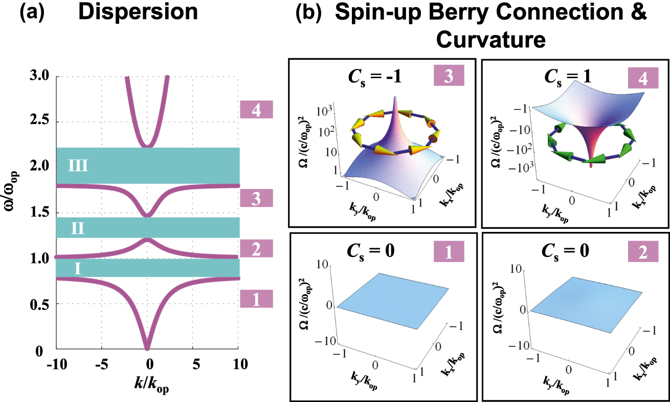
Topological phase in a bi-anisotropic (BI) PCM with electromagnetic (EM) duality
To study the topological properties of those bulk bands and gaps, we should attain the Berry information, including the Berry connection
where
The net Chern number always vanishes (i.e. C
+ + C
− = 0) due to time-reversal invariance. The topological phase of the overall system can be characterized by another invariant, i.e. spin Chern number
2.3 Topological phase transition characterized by electromagnetic parameters
In fact, regardless of band theory, the optical properties of PCM should be related to its EM parameters. This issue inspires us to bridge the gap between topological phase and EM parameters. We start with a fundamental parameter, i.e. the square of effective refractive index (SERI)
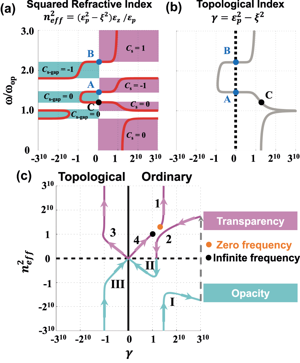
Characterization of topological phase transition based on electromagnetic parameters. (a) The square of effective refractive index (SERI)
As stated above, the transition of topological phase is related to the singularity of Berry curvature. The expression of Berry curvature can be analytically written as
where W
0 is proportional to the time-averaged energy density that W
0 > 0. To observe the distribution of Berry curvature and retrieve topologically nontrivial phase, all of the following discussions focus on nonzero BI coefficient. According to Equation (9), the Berry curvatures go to infinity when the term
On the other hand, we can apply the solutions of eigenfields [Eq. (S12) in the Supplementary Materials] to reveal the underlaying physics of topological index γ. Consider the eigenfields propagating along y axis (k x = 0), and the complex amplitude can be simplified as,
For ξ = 0, the eigenfields propagating along y axis are linearly polarized in x-z plane. For ξ ≠ 0, the eigenfields possess longitudinal component (
A topological phase map is defined to combine the information of SERI and topological index, as shown in Figure 1. The phase map can be divided into four quadrants, i.e. ordinary transparency, topological transparency, topological opacity and ordinary opacity. There are two types of topological transition highlighting by red arrows. As SERI
Here, we discuss the expandability of the proposal EM-parameter method, which applies the sign of in-plane constitutive difference
2.4 Relationship between pseudo surface impedance and topological phase
On the other hand, the surface impedance is related to the existence of interface states. Inspired by this method, we introduce the concept of surface impedance into the bi-anisotropic PCM. Figure 4a shows the definition of pseudo surface impedance on the downward side of the boundary as the ratio of the x-direction spin wave to the z-direction spin wave, yielding
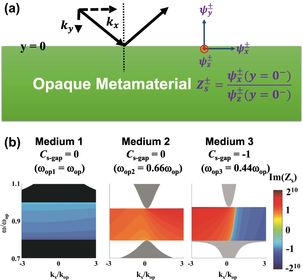
Relationship between pseudo surface impedance and topological phase. (a) Definition of pseudo surface impedance as the ratio of the x-direction spin wave to the z-direction spin wave. (b) Imaginary part of surface impedance for spin-up states in three different PCM, as the same EM parameters to Figure 2 except for normalized in-plane oscillation frequency. For simplicity, the pseudo surface impedances are only given in the opaque regions of each medium.
2.5 Optical propagation of topological edge states in PCM
Next, we will focus on the propagation of edge states forming by two diverse opacities. To get a better understanding of spinful edge states, we construct a one-dimensional interface along x axis formed between two semi-infinite materials. The edge dispersion for spin-up and -down can be presented as follows,
where the subscripts 1 and 2 represent the materials on each side of interface. ‘+’ and ‘-’ attribute to spin-up and spin-down cases, indicating they have opposite propagation direction for each other. After solving Eq. (11), we can obtain the edge dispersion at an interface between an C s = 0 ordinary opacity (medium 1) and a C s = −1 topological opacity (medium 3) in Figure 5a. As the time-reversal partners, the dispersions for spin-up (blue) and spin-down (red) edge states are symmetrical with respect to the plane of k x = 0, and gaplessly cross over the complete gap. Consequently, the rightward unidirectional propagation can be excited by a spin-up point source [blue vortex in Figure 5b], as expected from the bulk topology. Such spin-momentum locking property is the photonic analog of quantum spin Hall effect. Figure 5c–f show the simulation results (calculated by COMSOL Multiphysics) of optical propagation along the two interfaces, when the operation frequency of all excited source is ω = 0.9ω op. The topological edge state can be robust against the ‘SYSU’ shaped bending, as depicted in Figure 5c. The incident light couples to rightward wave and passes through the bending interface without backscattering, even though using a spinless E z-polarization source (black dot). For comparison, we also give a control case of gapped edge dispersion supported by an interface between two ordinary opacities (medium 1 and medium 2). Figure 5e and f have the same numerical setup to the left panel, except for topologically trivial interface. Due to lack of topological protection, the interface wave is failure against both unidirectional excitation and robust propagation.
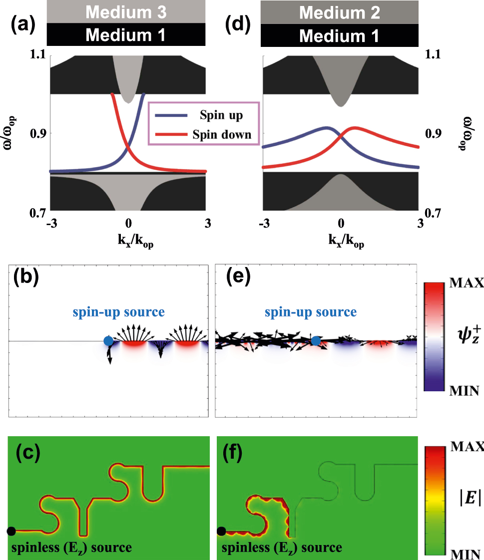
Optical propagation in topologically non-trivial (left) and trivial (right) interfaces. (a) Edge dispersion at an interface between an C s = 0 ordinary opacity (medium 1) and a C s = −1 topological opacity (medium 3). (b) Rightward unidirectional couple excited by a spin-up point source (blue dot). The black arrows represent the in-plane components (ψ x , ψ y ) of edge states. (c) Robust propagation of topological edge state against the ‘SYSU’ shaped bending, by using a spinless E z-polarization source (black dot). (d) Edge dispersion supported by an interface between two ordinary opacities (medium 1 and medium 2). (e) and (f) Same numerical setup to the left panel, except for topologically trivial interface.
Finally, we will discuss the possible experiment to mimic the topological interface above. Note that the bi-anisotropic metamaterials have been constructed by EM-dual ‘meta-atom’ between two metal plates [11], [55]. Similarly, we show the concrete designs to achieve the topologically non-trivial and trivial opacities in microwave regime [with the operation frequency from 2.0 to 2.5 GHz], which maintain EM duality and non-zero bianisotropy (see Appendix F of the Supplementary Materials). We have designed two types of meta-atoms in millimeter scale, where one of them is denoted by gyro-scope atom and the other is close-ring atom, to be homogenized as EM-dual PCMs. The analytic derivations prove that the first-order waveguide modes in EM-dual medium sandwiched by two perfect-electric-conductor (PEC) plates can render the strong effective bianisotropy ξ
eff
. When these two types of meta-atoms are placed inside the 38-mm-width PEC waveguides, the close-ring-atom waveguide serves as topologically non-trivial opacity due to its effective topological index
3 Conclusions
In summary, we have successfully applied a topological index based on EM parameters to demonstrate the topologically nontrivial properties in a class of 2D PCM with bi-anisotropic response. With an analytic deduction, we have concluded that the topology is determined by the sign of topological index. An example with Lorentz-like dispersion is given to verify this key point, including the evolution of topological index, pseudo surface impedance of bulk-edge correspondence, and topologically edge states. Since such index only depends on EM parameters, the proposal of EM-parameter method will benefit to simplify the design of topological metamaterial in some manner, and will lead to novel fundamental physics and device applications in the field of metamaterial.
Funding source: National Natural Science Foundation of China
Award Identifier / Grant number: 62035016
Award Identifier / Grant number: 12274475
Award Identifier / Grant number: 2023B1515040023
Award Identifier / Grant number: 2023B1515020072
-
Research funding: This work was supported by National Natural Science Foundation of China (62035016, 12274475), Basic and Applied Basic Research Foundation of Guangdong Province (2023B1515040023, 2023B1515020072).
-
Author contributions: All authors have accepted responsibility for the entire content of this manuscript and consented to its submission to the journal, reviewed all the results and approved the final version of the manuscript. XTH and JWD conceived the idea. XTH and SSZ developed the theory and performed simulations. XTH prepared the manuscript with contributions from all co-authors. JWD and XTH supervised the project.
-
Conflict of interest: Authors state no conflict of interest.
-
Data availability: The data that supports findings of this study are available from the corresponding author upon reasonable request.
References
[1] M. Hasan and C. Kane, “Colloquium: topological insulators,” Rev. Mod. Phys., vol. 82, no. 4, pp. 3045–3067, 2010. https://doi.org/10.1103/revmodphys.82.3045.Suche in Google Scholar
[2] X.-L. Qi and S.-C. Zhang, “Topological insulators and superconductors,” Rev. Mod. Phys., vol. 83, no. 4, pp. 1057–1110, 2011. https://doi.org/10.1103/revmodphys.83.1057.Suche in Google Scholar
[3] L. Lu, J. D. Joannopoulos, and M. Soljacic, “Topological photonics,” Nat. Photon., vol. 8, no. 11, pp. 821–829, 2014. https://doi.org/10.1038/nphoton.2014.248.Suche in Google Scholar
[4] A. B. Khanikaev and G. Shvets, “Two-dimensional topological photonics,” Nat. Photon., vol. 11, no. 12, pp. 763–773, 2017. https://doi.org/10.1038/s41566-017-0048-5.Suche in Google Scholar
[5] T. Ozawa, et al.., “Topological photonics,” Rev. Mod. Phys., vol. 91, no. 1, p. 015006, 2019. https://doi.org/10.1103/revmodphys.91.015006.Suche in Google Scholar
[6] M. Kim, Z. Jacob, and J. Rho, “Recent advances in 2D, 3D and higher-order topological photonics,” Light: Sci. Appl., vol. 9, no. 1, p. 130, 2020. https://doi.org/10.1038/s41377-020-0331-y.Suche in Google Scholar PubMed PubMed Central
[7] G. J. Tang, X. T. He, F. L. Shi, J. W. Liu, X. D. Chen, and J. W. Dong, “Topological photonic crystals: physics, designs, and applications,” Laser Photon. Rev., vol. 16, no. 4, p. 2100300, 2022. https://doi.org/10.1002/lpor.202100300.Suche in Google Scholar
[8] F. Haldane and S. Raghu, “Possible realization of directional optical waveguides in photonic crystals with broken time-reversal symmetry,” Phys. Rev. Lett., vol. 100, no. 1, p. 013904, 2008. https://doi.org/10.1103/physrevlett.100.013904.Suche in Google Scholar PubMed
[9] Z. Wang, Y. Chong, J. D. Joannopoulos, and M. Soljacic, “Observation of unidirectional backscattering-immune topological electromagnetic states,” Nature, vol. 461, no. 7265, pp. 772–775, 2009. https://doi.org/10.1038/nature08293.Suche in Google Scholar PubMed
[10] A. B. Khanikaev, S. Hossein Mousavi, W.-K. Tse, M. Kargarian, A. H. MacDonald, and G. Shvets, “Photonic topological insulators,” Nat. Mater., vol. 12, no. 3, pp. 233–239, 2013. https://doi.org/10.1038/nmat3520.Suche in Google Scholar PubMed
[11] W.-J. Chen, et al.., “Experimental realization of photonic topological insulator in a uniaxial metacrystal waveguide,” Nat. Commun., vol. 5, no. 1, p. 5782, 2014. https://doi.org/10.1038/ncomms6782.Suche in Google Scholar PubMed
[12] C. He, et al.., “Photonic topological insulator with broken time-reversal symmetry,” Proc. Natl. Acad. Sci., vol. 113, no. 18, pp. 4924–4928, 2016. https://doi.org/10.1073/pnas.1525502113.Suche in Google Scholar PubMed PubMed Central
[13] M. Hafezi, S. Mittal, J. Fan, A. Migdall, and J. M. Taylor, “Imaging topological edge states in silicon photonics,” Nat. Photon., vol. 7, no. 12, pp. 1001–1005, 2013. https://doi.org/10.1038/nphoton.2013.274.Suche in Google Scholar
[14] L.-H. Wu and X. Hu, “Scheme for achieving a topological photonic crystal by using dielectric material,” Phys. Rev. Lett., vol. 114, no. 22, p. 223901, 2015. https://doi.org/10.1103/physrevlett.114.223901.Suche in Google Scholar
[15] S. Barik, et al.., “A topological quantum optics interface,” Science, vol. 359, no. 6376, pp. 666–668, 2018. https://doi.org/10.1126/science.aaq0327.Suche in Google Scholar PubMed
[16] S. Barik, H. Miyake, W. DeGottardi, E. Waks, and M. Hafezi, “Two-dimensionally confined topological edge states in photonic crystals,” New J. Phys., vol. 18, no. 11, p. 113013, 2016. https://doi.org/10.1088/1367-2630/18/11/113013.Suche in Google Scholar
[17] T. Ma and G. Shvets, “All-Si valley-Hall photonic topological insulator,” New J. Phys., vol. 18, no. 2, p. 025012, 2016. https://doi.org/10.1088/1367-2630/18/2/025012.Suche in Google Scholar
[18] J.-W. Dong, X.-D. Chen, H. Zhu, Y. Wang, and X. Zhang, “Valley photonic crystals for control of spin and topology,” Nat. Mater., vol. 16, no. 3, pp. 298–302, 2017. https://doi.org/10.1038/nmat4807.Suche in Google Scholar PubMed
[19] X.-D. Chen, F.-L. Zhao, M. Chen, and J.-W. Dong, “Valley-contrasting physics in all-dielectric photonic crystals: orbital angular momentum and topological propagation,” Phys. Rev. B, vol. 96, no. 2, p. 020202(R), 2017. https://doi.org/10.1103/physrevb.96.020202.Suche in Google Scholar
[20] M. I. Shalaev, W. Walasik, A. Tsukernik, Y. Xu, and N. M. Litchinitser, “Robust topologically protected transport in photonic crystals at telecommunication wavelengths,” Nat. Nanotechnol., vol. 14, no. 1, pp. 31–34, 2019. https://doi.org/10.1038/s41565-018-0297-6.Suche in Google Scholar PubMed
[21] X.-T. He, et al.., “A silicon-on-insulator slab for topological valley transport,” Nat. Commun., vol. 10, no. 1, p. 872, 2019. https://doi.org/10.1038/s41467-019-08881-z.Suche in Google Scholar PubMed PubMed Central
[22] M. Xiao, Z. Q. Zhang, and C. T. Chan, “Surface impedance and bulk band geometric phases in one-dimensional systems,” Phys. Rev. X, vol. 4, no. 2, p. 021017, 2014. https://doi.org/10.1103/physrevx.4.021017.Suche in Google Scholar
[23] F. Liu and K. Wakabayashi, “Novel topological phase with a zero berry curvature,” Phys. Rev. Lett., vol. 118, no. 7, p. 076803, 2017. https://doi.org/10.1103/physrevlett.118.076803.Suche in Google Scholar PubMed
[24] B.-Y. Xie, et al.., “Second-order photonic topological insulator with corner states,” Phys. Rev. B, vol. 98, no. 20, p. 205147, 2018. https://doi.org/10.1103/physrevb.98.205147.Suche in Google Scholar
[25] B.-Y. Xie, et al.., “Visualization of higher-order topological insulating phases in two-dimensional dielectric photonic crystals,” Phys. Rev. Lett., vol. 122, no. 23, p. 233903, 2019. https://doi.org/10.1103/physrevlett.122.233903.Suche in Google Scholar
[26] X.-D. Chen, W.-M. Deng, F.-L. Shi, F.-L. Zhao, M. Chen, and J.-W. Dong, “Direct observation of corner States in second-order topological photonic crystal slabs,” Phys. Rev. Lett., vol. 122, no. 23, p. 233902, 2019. https://doi.org/10.1103/physrevlett.122.233902.Suche in Google Scholar PubMed
[27] A. El Hassan, F. K. Kunst, A. Moritz, G. Andler, E. J. Bergholtz, and M. Bourennane, “Corner states of light in photonic waveguides,” Nat. Photon., vol. 13, no. 10, pp. 697–700, 2019. https://doi.org/10.1038/s41566-019-0519-y.Suche in Google Scholar
[28] Y. Ota, et al.., “Photonic crystal nanocavity based on a topological corner state,” Optica, vol. 6, no. 6, pp. 786–789, 2019. https://doi.org/10.1364/optica.6.000786.Suche in Google Scholar
[29] J. Noh, et al.., “Topological protection of photonic mid-gap defect modes,” Nat. Photon., vol. 12, no. 7, pp. 408–415, 2018. https://doi.org/10.1038/s41566-018-0179-3.Suche in Google Scholar
[30] C. W. Peterson, W. A. Benalcazar, T. L. Hughes, and G. Bahl, “A quantized microwave quadrupole insulator with topologically protected corner states,” Nature, vol. 555, no. 7696, pp. 346–350, 2018. https://doi.org/10.1038/nature25777.Suche in Google Scholar PubMed
[31] M. Serra-Garcia, et al.., “Observation of a phononic quadrupole topological insulator,” Nature, vol. 555, no. 7696, pp. 342–345, 2018. https://doi.org/10.1038/nature25156.Suche in Google Scholar PubMed
[32] G. Harari, et al.., “Topological insulator laser: theory,” Science, vol. 359, no. 6381, p. eaar4003, 2018. https://doi.org/10.1126/science.aar4003.Suche in Google Scholar PubMed
[33] M. A. Bandres, et al.., “Topological insulator laser: experiments,” Science, vol. 359, no. 6381, p. eaar4005, 2018. https://doi.org/10.1126/science.aar4005.Suche in Google Scholar PubMed
[34] A. Blanco-Redondo, B. Bell, D. Oren, B. J. Eggleton, and M. Segev, “Topological protection of biphoton states,” Science, vol. 362, no. 6414, p. 568, 2018. https://doi.org/10.1126/science.aau4296.Suche in Google Scholar PubMed
[35] S. Mittal, E. A. Goldschmidt, and M. Hafezi, “A topological source of quantum light,” Nature, vol. 561, no. 7724, pp. 502–506, 2018. https://doi.org/10.1038/s41586-018-0478-3.Suche in Google Scholar PubMed
[36] A. Bansil, H. Lin, and T. Das, “Colloquium: topological band theory,” Rev. Mod. Phys., vol. 88, no. 2, p. 021004, 2016. https://doi.org/10.1103/revmodphys.88.021004.Suche in Google Scholar
[37] J. D. Joannopoulos, S. G. Johnson, J. N. Winn, and R. D. Meade, Photonic Crystals: Molding the Flow of Light, New Jersey, Princeton university press, 2011.10.2307/j.ctvcm4gz9Suche in Google Scholar
[38] C. M. Soukoulis and M. Wegener, “Past achievements and future challenges in the development of three-dimensional photonic metamaterials,” Nat. Photon., vol. 5, no. 9, pp. 523–530, 2011. https://doi.org/10.1038/nphoton.2011.154.Suche in Google Scholar
[39] S. Jahani and Z. Jacob, “All-dielectric metamaterials,” Nat. Nanotech., vol. 11, no. 1, pp. 23–36, 2016. https://doi.org/10.1038/nnano.2015.304.Suche in Google Scholar PubMed
[40] Z. Yu, G. Veronis, Z. Wang, and S. Fan, “One-Way electromagnetic waveguide formed at the interface between a plasmonic metal under a static magnetic field and a photonic crystal,” Phys. Rev. Lett., vol. 100, no. 2, p. 023902, 2008. https://doi.org/10.1103/physrevlett.100.023902.Suche in Google Scholar
[41] A. Davoyan and N. Engheta, “Theory of wave propagation in magnetized near-zero-epsilon metamaterials: evidence for one-way photonic States and magnetically switched transparency and opacity,” Phys. Rev. Lett., vol. 111, no. 25, p. 257401, 2013. https://doi.org/10.1103/physrevlett.111.257401.Suche in Google Scholar PubMed
[42] M. G. Silveirinha, “Chern invariants for continuous media,” Phys. Rev. B, vol. 92, no. 12, p. 125153, 2015. https://doi.org/10.1103/physrevb.92.125153.Suche in Google Scholar
[43] M. G. Silveirinha, “P·T·Dsymmetry-protected scattering anomaly in optics,” Phys. Rev. B, vol. 95, no. 3, p. 035153, 2017. https://doi.org/10.1103/physrevb.95.035153.Suche in Google Scholar
[44] W. Gao, et al.., “Topological photonic phase in chiral hyperbolic metamaterials,” Phys. Rev. Lett., vol. 114, no. 3, p. 037402, 2015. https://doi.org/10.1103/physrevlett.114.037402.Suche in Google Scholar PubMed
[45] M. Xiao, Q. Lin, and S. Fan, “Hyperbolic Weyl point in reciprocal chiral metamaterial,” Phys. Rev. Lett., vol. 117, no. 5, p. 057401, 2016. https://doi.org/10.1103/physrevlett.117.057401.Suche in Google Scholar PubMed
[46] F. Zangeneh-Nejad and R. Fleury, “Zero-Index weyl metamaterials,” Phys. Rev. Lett., vol. 125, no. 5, p. 054301, 2020. https://doi.org/10.1103/physrevlett.125.054301.Suche in Google Scholar PubMed
[47] B. Yang, et al.., “Ideal Weyl points and helicoid surface states in artificial photonic crystal structures,” Science, vol. 359, no. 6379, pp. 1013–1016, 2018. https://doi.org/10.1126/science.aaq1221.Suche in Google Scholar PubMed
[48] S. Ma, et al.., “Linked Weyl surfaces and Weyl arcs in photonic metamaterials,” Science, vol. 373, no. 6554, pp. 572–576, 2021. https://doi.org/10.1126/science.abi7803.Suche in Google Scholar PubMed
[49] C. He, L. Zhao, S. Zhang, L. Zhou, and S. Ma, “Intrinsic topological Hinge states induced by boundary gauge fields in photonic metamaterials,” eLight, vol. 5, no. 1, p. 19, 2025. https://doi.org/10.1186/s43593-025-00097-7.Suche in Google Scholar
[50] S. A. R. Horsley and M. Woolley, “Zero-refractive-index materials and topological photonics,” Nat. Phys., vol. 17, no. 3, pp. 348–355, 2021. https://doi.org/10.1038/s41567-020-01082-2.Suche in Google Scholar
[51] R.-Y. Zhang, et al.., “Bulk–spatiotemporal vortex correspondence in gyromagnetic zero-index media,” Nature, vol. 641, no. 8065, pp. 1142–1148, 2025. https://doi.org/10.1038/s41586-025-08948-6.Suche in Google Scholar PubMed
[52] S. Lannebère and M. G. Silveirinha, “Photonic analogues of the Haldane and Kane-Mele models,” Nanophotonics, vol. 8, no. 8, pp. 1387–1397, 2019. https://doi.org/10.1515/nanoph-2019-0037.Suche in Google Scholar
[53] E. Lustig, et al.., “Photonic topological insulator in synthetic dimensions,” Nature, vol. 567, no. 7748, pp. 356–360, 2019. https://doi.org/10.1038/s41586-019-0943-7.Suche in Google Scholar PubMed
[54] D. Yu, et al.., “Comprehensive review on developments of synthetic dimensions,” Photon. Insights, vol. 4, no. 2, p. R06, 2025. https://doi.org/10.3788/pi.2025.r06.Suche in Google Scholar
[55] A. P. Slobozhanyuk, A. B. Khanikaev, D. S. Filonov, D. A. Smirnova, A. E. Miroshnichenko, and Y. S. Kivshar, “Experimental demonstration of topological effects in bianisotropic metamaterials,” Sci. Rep., vol. 6, no. 1, p. 22270, 2016. https://doi.org/10.1038/srep22270.Suche in Google Scholar PubMed PubMed Central
Supplementary Material
This article contains supplementary material (https://doi.org/10.1515/nanoph-2025-0451).
© 2025 the author(s), published by De Gruyter, Berlin/Boston
This work is licensed under the Creative Commons Attribution 4.0 International License.
Artikel in diesem Heft
- Frontmatter
- Reviews
- Light-driven micro/nanobots
- Tunable BIC metamaterials with Dirac semimetals
- Large-scale silicon photonics switches for AI/ML interconnections based on a 300-mm CMOS pilot line
- Perspective
- Density-functional tight binding meets Maxwell: unraveling the mysteries of (strong) light–matter coupling efficiently
- Letters
- Broadband on-chip spectral sensing via directly integrated narrowband plasmonic filters for computational multispectral imaging
- Sub-100 nm manipulation of blue light over a large field of view using Si nanolens array
- Tunable bound states in the continuum through hybridization of 1D and 2D metasurfaces
- Integrated array of coupled exciton–polariton condensates
- Disentangling the absorption lineshape of methylene blue for nanocavity strong coupling
- Research Articles
- Demonstration of multiple-wavelength-band photonic integrated circuits using a silicon and silicon nitride 2.5D integration method
- Inverse-designed gyrotropic scatterers for non-reciprocal analog computing
- Highly sensitive broadband photodetector based on PtSe2 photothermal effect and fiber harmonic Vernier effect
- Online training and pruning of multi-wavelength photonic neural networks
- Robust transport of high-speed data in a topological valley Hall insulator
- Engineering super- and sub-radiant hybrid plasmons in a tunable graphene frame-heptamer metasurface
- Near-unity fueling light into a single plasmonic nanocavity
- Polarization-dependent gain characterization in x-cut LNOI erbium-doped waveguide amplifiers
- Intramodal stimulated Brillouin scattering in suspended AlN waveguides
- Single-shot Stokes polarimetry of plasmon-coupled single-molecule fluorescence
- Metastructure-enabled scalable multiple mode-order converters: conceptual design and demonstration in direct-access add/drop multiplexing systems
- High-sensitivity U-shaped biosensor for rabbit IgG detection based on PDA/AuNPs/PDA sandwich structure
- Deep-learning-based polarization-dependent switching metasurface in dual-band for optical communication
- A nonlocal metasurface for optical edge detection in the far-field
- Coexistence of weak and strong coupling in a photonic molecule through dissipative coupling to a quantum dot
- Mitigate the variation of energy band gap with electric field induced by quantum confinement Stark effect via a gradient quantum system for frequency-stable laser diodes
- Orthogonal canalized polaritons via coupling graphene plasmon and phonon polaritons of hBN metasurface
- Dual-polarization electromagnetic window simultaneously with extreme in-band angle-stability and out-of-band RCS reduction empowered by flip-coding metasurface
- Record-level, exceptionally broadband borophene-based absorber with near-perfect absorption: design and comparison with a graphene-based counterpart
- Generalized non-Hermitian Hamiltonian for guided resonances in photonic crystal slabs
- A 10× continuously zoomable metalens system with super-wide field of view and near-diffraction–limited resolution
- Continuously tunable broadband adiabatic coupler for programmable photonic processors
- Diffraction order-engineered polarization-dependent silicon nano-antennas metagrating for compact subtissue Mueller microscopy
- Lithography-free subwavelength metacoatings for high thermal radiation background camouflage empowered by deep neural network
- Multicolor nanoring arrays with uniform and decoupled scattering for augmented reality displays
- Permittivity-asymmetric qBIC metasurfaces for refractive index sensing
- Theory of dynamical superradiance in organic materials
- Second-harmonic generation in NbOI2-integrated silicon nitride microdisk resonators
- A comprehensive study of plasmonic mode hybridization in gold nanoparticle-over-mirror (NPoM) arrays
- Foundry-enabled wafer-scale characterization and modeling of silicon photonic DWDM links
- Rough Fabry–Perot cavity: a vastly multi-scale numerical problem
- Classification of quantum-spin-hall topological phase in 2D photonic continuous media using electromagnetic parameters
- Light-guided spectral sculpting in chiral azobenzene-doped cholesteric liquid crystals for reconfigurable narrowband unpolarized light sources
- Modelling Purcell enhancement of metasurfaces supporting quasi-bound states in the continuum
- Ultranarrow polaritonic cavities formed by one-dimensional junctions of two-dimensional in-plane heterostructures
- Bridging the scalability gap in van der Waals light guiding with high refractive index MoTe2
- Ultrafast optical modulation of vibrational strong coupling in ReCl(CO)3(2,2-bipyridine)
- Chirality-driven all-optical image differentiation
- Wafer-scale CMOS foundry silicon-on-insulator devices for integrated temporal pulse compression
- Monolithic temperature-insensitive high-Q Ta2O5 microdisk resonator
- Nanogap-enhanced terahertz suppression of superconductivity
- Large-gap cascaded Moiré metasurfaces enabling switchable bright-field and phase-contrast imaging compatible with coherent and incoherent light
- Synergistic enhancement of magneto-optical response in cobalt-based metasurfaces via plasmonic, lattice, and cavity modes
- Scalable unitary computing using time-parallelized photonic lattices
- Diffusion model-based inverse design of photonic crystals for customized refraction
- Wafer-scale integration of photonic integrated circuits and atomic vapor cells
- Optical see-through augmented reality via inverse-designed waveguide couplers
- One-dimensional dielectric grating structure for plasmonic coupling and routing
- MCP-enabled LLM for meta-optics inverse design: leveraging differentiable solver without LLM expertise
- Broadband variable beamsplitter made of a subwavelength-thick metamaterial
- Scaling-dependent tunability of spin-driven photocurrents in magnetic metamaterials
- AI-based analysis algorithm incorporating nanoscale structural variations and measurement-angle misalignment in spectroscopic ellipsometry