Broadband on-chip spectral sensing via directly integrated narrowband plasmonic filters for computational multispectral imaging
-
Qilin Zheng

 ,
Li Liang
,
Li Liang

Abstract
Spectroscopy underpins a wide range of applications, including biomedical diagnostics, precision agriculture, remote sensing, and industrial process control. Recent advances in silicon and microwave photonic integration have facilitated the miniaturization of spectroscopic systems, enabling portable, real-time analysis. However, the realization of a chip-scale platform that simultaneously achieves broadband coverage, high resolution, and scalable low-cost fabrication – particularly in the near-infrared (NIR) regime – remains a significant challenge. Here, we present a compact and cost-effective NIR spectroscopic sensing chip that monolithically integrates a plasmonic bandpass filter array with InGaAs photodetectors. The device is fabricated via single-step lithography and features a nanohole array with geometrically tunable narrowband transmission spanning 900–1,700 nm, exhibiting a full width at half maximum (FWHM) of 5.0 nm and a peak Q-factor of ∼284. The plasmonic filters are directly integrated with the detectors through a SiN x spacer layer, eliminating post-fabrication alignment and enhancing scalability. A 16-channel super-pixel layout, combined with computational spectral reconstruction, enables ∼1 nm resolution near 1,550 nm and supports high-fidelity spectral imaging. This work demonstrates a scalable, detector-compatible approach to on-chip NIR spectroscopy, offering a promising route toward deployable, compact spectral sensing platforms.
1 Introduction
Spectroscopic sensing technologies offer high precision, low latency, imaging capability, and multidimensional detection, making them indispensable in critical fields such as remote sensing, geological exploration, petrochemical processing, industrial inspection, and biomedical diagnostics [1], [2], [3], [4]. Near-infrared (NIR) spectroscopy has garnered significant attention in biomedical applications due to its rich biochemical fingerprint features [5], [6], [7], [8]. Since the 1990s, NIR spectroscopy has evolved into a core analytical tool across agriculture, medicine, environmental monitoring, and food safety, valued for its non-destructive, rapid, and highly sensitive detection capabilities [9], [10], [11]. The advancement of micro/nanophotonics and information technology, coupled with the growing demand for compact, lightweight platforms – such as unmanned aerial vehicles and wearable devices – has accelerated the miniaturization and integration of optical sensors [12], [13]. However, current spectrometers are largely based on bulky and expensive benchtop systems, such as Fourier-transform infrared (FTIR) and grating-based NIR spectrometers, which are poorly suited for in-field or mobile applications. This limitation has hindered the widespread adoption of NIR spectroscopy in practical scenarios [1].
Recent developments in nanophotonic and microfabrication technologies have opened new avenues for chip-scale spectroscopic sensing. These structures enable precise subwavelength light manipulation and enhanced light–matter interaction, promising high sensitivity and resolution in a significantly reduced footprint [14]. Nevertheless, many miniaturized designs primarily focus on physical downscaling without fundamentally rethinking the optical architecture, often resulting in compromised performance. For instance, miniaturized diffraction gratings typically suffer from reduced spectral dispersion efficiency and signal-to-noise ratio, exposing a key challenge: achieving high resolution and sensitivity in space-constrained systems. Computational spectrometers-on-chip have emerged as a promising solution, harnessing algorithmic reconstruction to decouple system performance from physical constraints [15], [16], [17], [18], [19], [20], [21], [22], [23], [24], [25]. These devices leverage advanced materials and micro/nanostructures, along with machine learning and signal processing, to enable integrated and reconfigurable spectroscopic functionality. Research in this area broadly falls into two directions: advanced materials and advanced nano-optical structure.
In the realm of materials innovation, bandgap-tunable nanomaterials offer powerful routes to spectral selectivity. Techniques such as compositional tuning [26], [27], bias-induced modulation [28], [29], phase-change materials [30], and organic semiconductors [31] have enabled tunable spectral responses. For instance, Bao et al. developed a miniaturized spectrometer using 195 types of colloidal quantum dots (CQDs) integrated with CCDs, achieving tunable bandgaps over a 300 nm range [26]. Yang et al. synthesized CdS x Se1−x nanowires with a spatially varying bandgap from 1.74 to 2.42 eV, enabling 10 nm resolution across 500–630 nm [27]. Sun et al. demonstrated bias-controlled perovskite photodetectors for spectral tuning via ion migration, achieving ∼5 nm resolution [27]. In the mid-infrared, Kim et al. employed Ge2Sb2Te5 (GST) phase-change materials within plasmonic nanohole arrays to realize broadband spectral tuning across 2.91–3.41 μm [30]. Other approaches include exploiting van der Waals heterostructures [28], [29], heavy-metal atom doping [32], and organic narrowband absorbers [31]. However, many of these materials face challenges in stability, scalability, or fabrication complexity.
In advanced nano-optical structure, innovative photonic designs have demonstrated high-performance on-chip spectral filtering. For example, Cao et al. used helical waveguides in multimode planar waveguides to enhance optical path length, achieving 10 pm resolution within a 20 nm band [33]. CMOS-compatible dielectric metasurfaces have also shown great potential. Altug et al. integrated multispectral resonant metasurfaces with CMOS platforms, enabling high-resolution biosensing without mechanical scanning [34], [35]. Disordered nanohole arrays etched on SOI substrates have yielded 0.75 nm resolution at 1,550 nm via light scattering in photonic crystals, although their coupling efficiency remains limited [36]. Yu et al. employed photonic crystal slab arrays to couple incident light into in-plane propagation modes, forming random spectral fingerprints for compressed sensing, achieving 1 nm resolution with improved efficiency [37], [38]. Despite these advances, high-precision nanostructures typically demand strict control over geometric parameters, such as nanopillar diameter and periodicity, which poses scalability challenges. Moreover, compared to the visible range, progress in integrated infrared spectroscopy has been slower due to the high cost of focal plane arrays and the complexity of integrating IR-compatible spectral filters on-chip [3], [7], [19], [39]. These factors limit practical deployment in cost-sensitive or mobile environments.
With the rapid evolution of machine learning and computational optics, highly customized, low-channel-count spectrometers are becoming increasingly practical and economically viable. In this study, we report the development of a wafer-scale, low-noise plasmonic bandpass filter array operable from 900 to 1,700 nm. Fabricated via a single lithographic step, the array provides multiple passbands for integrated spectral sampling (Figure 1). We further direct integrate the filters with InGaAs photodetector arrays to form a compact 16-channel spectroscopic sensor with ∼1 nm resolution around 1,550 nm. Finally, we demonstrate computational spectral reconstruction and multispectral imaging, showcasing its potential as a scalable and multifunctional platform for near-infrared spectroscopic sensing.

Conceptual diagram of the proposed broadband on-chip spectral sensing system. The spectral-spatial information of an object (L(x, y, λ), e.g., a tree scene) is converted to a 2D photocurrent map I (x, y) through a monolithically integrated chip f i (λ). This system features a vertically integrated architecture: Top: period-tunable plasmonic narrowband filter array implementing pixel-specific spectral encoding. Bottom: InGaAs photodetector array directly converting filtered light into electrical intensity signals.
2 Results
2.1 Narrowband near – infrared plasmonic bandpass transmission filter
For on-chip spectroscopy, a high-efficiency narrowband bandpass filter operating across a broad wavelength range with low background has long been pursued as a pivotal component. We developed a novel plasmonic bandpass filter with simple architecture and direct detector integrability, comprising a dielectric nanohole array perforated in a thin metal film (Figure 2a). The resonant response arises from surface plasmon polariton excitation by the periodic nanohole array at the metal–dielectric interface [30], [40]. Shallow nanoholes (H < 80 nm) suppress out-of-plane radiative leakage, yielding a narrow transmission linewidth (FWHM < 10 nm). The optical response is primarily governed by three structural parameters: (i) Etching depth (H), which influences mode confinement and propagation loss; (ii) Au film thickness (t Au), which affects coupling efficiency and Ohmic dissipation; and (iii) Filling factor (FF = d/P, where d is the nanohole diameter and P is the period), which regulates inter-hole coupling and lattice diffraction. As quantitatively shown in Figures S1–3, these parameters collectively modulate the balance between resonant enhancement and intrinsic losses in the Au/SiN x heterostructure, enabling wavelength-specific narrowband filtering across 900–1,700 nm. As shown in Figure 2b, a transmittance exceeding 55 % can be maintained while achieving an FWHM as narrow as 5 nm. Furthermore, the central wavelength of the bandpass filter can be precisely tuned by varying the nanohole periodicity, enabling wafer-scale fabrication of filter arrays through a single lithographic step.

Period tunable narrowband near – infrared plasmonic bandpass transmission filters. (a) Schematic cross-section of the Au/SiN x nanohole array structure. (b) Simulated transmission spectra for the device structure in (a). The nanohole period P = 1,500 nm, the depth H = 70 nm, the Au film thickness t Au = 25 nm, and the fill factor FF = 0.7. Electric field distributions of device at characteristic wavelengths, I. xy-plane field intensity at 1,305 nm resonance wavelength (aperture center plane); II. xz-plane cross-section at 1,305 nm, illustrating the SPP resonance at the Au/SiN x boundary within the nanohole array; III. xy-plane distribution at 1,500 nm off-resonance wavelength (>80 % intensity reduction); IV. xz-plane profile at 1,500 nm, showing the absence of boundary electric field enhancement under off-resonance conditions. (c) Calculated transmission spectra of filter arrays at H = 70 nm, t Au = 30 nm and FF = 0.7. Chip is a 16-unit array with P = 1,050, 1,106, …, 1,950 nm. (d) The transmission spectra of the 16-period nanohole of the coefficient correlation matrix.
Building upon the optimized geometric parameters (H = 70 nm, t Au = 25 nm, FF = 0.7, P = 1,500 nm), we numerically validated the plasmonic resonance filter via full-field electromagnetic simulations. Figure 2b demonstrates exceptional narrowband filtering across a 900–1,700 nm operational window: >55 % peak transmittance at resonance Ultra-narrow bandwidth (FWHM ≈ 5 nm, Q ≈ 130) Strong out-of-band rejection (<10 % transmittance at off-resonance wavelengths) Field confinement analysis reveals the physical origin: at resonance (1,310 nm), surface plasmon polaritons (SPPs) couple to Au-dielectric interfaces within the nanoholes, generating intense near-field enhancement (|E|/|E 0| > 5.8). Conversely, off-resonance fields (1,500 nm) exhibit suppressed transmission (<10 %), confirming effective bandpass functionality. To extend spectral coverage, we engineered nanohole arrays with linearly scaled periods (P = 1.05–1.95 μm), achieving 16 discrete channels that quasi-continuously cover 900–1,700 nm (Figure 2c). This design enables computational spectrometry by constructing a high-dimensional spectral transfer matrix. Crucially, we evaluate the matrix quality through cross-correlation [2] analysis:
where f i (λ) denotes the transmission spectrum of the i-th (or j-th) filter, and C ij quantifies the spectral orthogonality between channels, which forms the basis for high-accuracy spectral reconstruction. As quantified by the correlation matrix in Figure 3d, the filters exhibit ultra-low mutual correlation with a mean cross-correlation coefficient of 0.25.
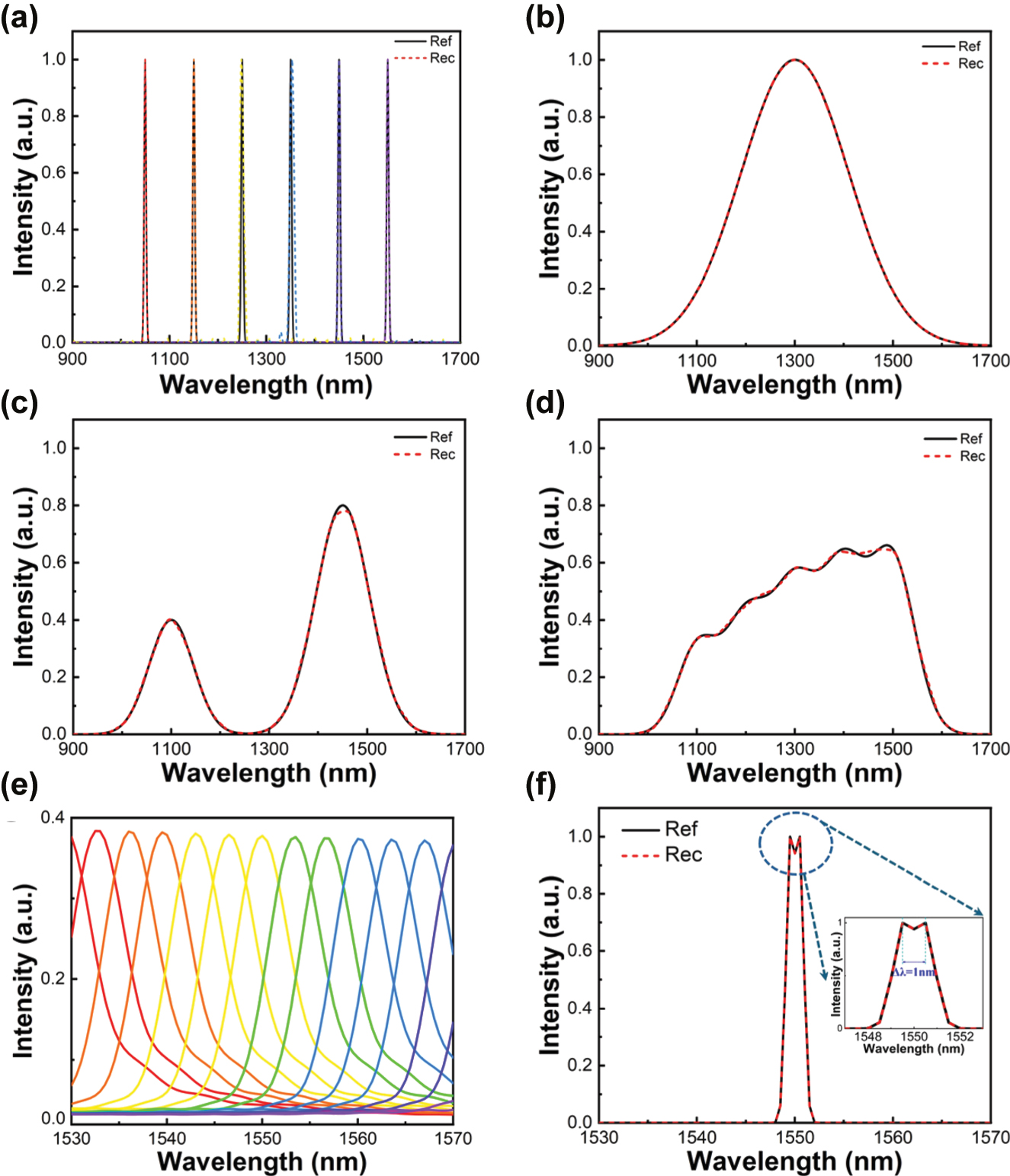
Spectral reconstruction comparisons to the reference spectrum. (a) Reconstructed target narrowband spectra (dotted lines, FWHM = 5 nm) using calculated filter responses as shown in Figure 3c. The black lines are the reference spectra. (b) Reconstructed single Gaussian peak target spectra (dotted lines, FWHM = 260 nm); (c) reconstructed two different half-width combinations target spectra (dotted lines, FWHM = 107/132 nm); (d) reconstructed target broadband spectra. (e) Transmission spectra generated by sixteen filter units with lattice periods ranging from 1.76 to 1.81 µm, covering the spectral range of 1,520–1,560 nm. (f) Reconstruction of a dual-peak signal centered at 1,550 nm with a 1 nm wavelength separation. The dashed box highlights the magnified view of the dual-peak region.
Infrared spectroscopy provides critical molecular fingerprint identification for portable precision matter analysis. While rich in chemical information, conventional infrared spectrometers suffer from bulkiness, complexity, and high cost. Emerging Computational Spectroscopy chip-scale alternatives offer compelling advantages: ultracompact footprint, simplified optics, and high accuracy. Crucially, spectrometer performance hinges on two parameters: operational bandwidth and spectral resolution, both fundamentally governed by the filtering subsystem. Here, we introduce a plasmonic nanohole array serving as an integrated tunable filter that simultaneously delivers: Narrow linewidth (FWHM ≈ 5 nm, Q max ≈ 284), broadband coverage (900–1,700 nm), high out-of-band rejection (>90 % suppression), enabling miniaturized computational spectrometers (Figure 2c).
Conventional grating spectrometers rely on spatially separated dispersive elements and long optical paths, with their resolution fundamentally constrained by detector pixel density. In contrast, our design integrates a periodically tunable transmission filter directly with the photodetector, thereby overcoming this limitation. This integration significantly reduces system complexity and footprint by eliminating bulky optical components. When paired with computational reconstruction, the architecture overcomes conventional resolution limits imposed by detector geometry.
Spectral reconstruction methodology:
For N = 16 filter channels spanning 900–1,700 nm (Figure 2c), the detector response is modeled as:
Here, L(λ) represents the target spectrum within the 900–1,700 nm range, while f i (λ) denotes the transmission response of the i-th plasmonic filter. The output signal from each detector corresponds to the convolution of L(λ) with its respective filter response. To construct the full sensing matrix, we precisely characterized f i (λ) using a wavelength-swept supercontinuum laser, scanning from 900 to 1,700 nm in 1-nm increments and recording each filter’s photoresponse. Recovering L(λ) from this under sampled dataset constitutes an ill-posed inverse problem, requiring advanced reconstruction techniques. To mitigate the influence of noise measurement, we apply L 2-norm Tikhonov regularization for robust spectral reconstruction from undersampled data [22], [41]. The modified Tikhonov formulation employed in our work is given by:
where α is the regularization weight value, and Γ is the auxiliary matrix. As demonstrated in Figure 3a–d, the recovered spectra closely match the reference in both peak location and general profile, with only minor deviations. To quantitatively assess reconstruction accuracy, we use spectral fidelity, defined as:
where x
i
and
To evaluate the spectral resolution of our approach, we reconstructed a synthetic spectrum containing two closely spaced narrowband peaks (Δλ = 1 nm) using the single-resonance response of our plasmonic filter structure, as shown in Figure 3f. Sixteen filter units, with periods ranging from 1.76 to 1.81 µm, were employed to generate transmission spectra spanning 1,520–1,560 nm (Figure 3e). Applying our reconstruction framework, we successfully resolved the characteristic double-peak profile using only 16 measurements, demonstrating the system’s high resolution. These results highlight the strong spectral discrimination capability of our plasmonic filter–InGaAs detector integrated chip, underscoring its potential for compact, on-site spectroscopic applications such as on-site material rapid inspection and point-of-care diagnostics.
Building on the high-fidelity spectral reconstruction framework used in Figure 3, we further extend the plasmonic filter–detector integrated chip toward on-chip multispectral imaging, enabling spatially resolved spectral acquisition within a compact platform. This architecture uniquely combines: Monolithic integration of tunable nanohole filters with InGaAs photodiodes, computational multiplexing enabled by the 16-channel filters, snapshot spatial-spectral capture without mechanical scanning. Hyperspectral dataset validation: As shown in Figure 4a, a hyperspectral image consisting of 463 × 241 pixels across 76 spectral bands (900–1,700 nm) was reconstructed based on the HYPERION dataset acquired over Jiangsu Province, China, on May 3, 2013 [42]. This dataset, primarily intended for monitoring fluvial material variations, demands highly accurate and faithful spectral image reconstruction. Using the 16 filter channels described in Figure 2c, we performed pixel-wise spectral reconstruction across the full dataset. Figure 4b–d present representative spectra at three distinct locations, where the reconstructed results closely match the reference spectra, achieving a spectral fidelity greater than 0.99. In addition, spectral images at eight representative wavelengths were visualized, demonstrating excellent boundary fidelity of the river morphology and clearly delineated shoreline features (Figure 4e). Furthermore, silicon-based hot-carrier photodetectors offer a promising alternative to InGaAs detectors in the near-infrared range, substantially reducing cost and improving compatibility with standard semiconductor fabrication processes. In addition, the filter design exhibits strong spectral scalability: by tuning the structural period P, the operational band can be readily reconfigured to target specific wavelength ranges. Together, these results establish our chip-based platform as a compact and scalable solution for next-generation airborne or field-deployable imaging spectrometers.
![Figure 4:
Hyperspectral imaging using the narrowband near-infrared plasmonic bandpass transmission filter spectrometer. (a) Hyperspectral data set of river image on May 3rd, 2013 [42]. (b–d) Recovered reflectance spectra (dotted lines) of three selected patches in the test multispectral image Figure 4a, the black lines are the reference spectra; (e) a series of reconstructed images at selected wavelengths. The intensity range of these images is normalized.](/document/doi/10.1515/nanoph-2025-0398/asset/graphic/j_nanoph-2025-0398_fig_004.jpg)
Hyperspectral imaging using the narrowband near-infrared plasmonic bandpass transmission filter spectrometer. (a) Hyperspectral data set of river image on May 3rd, 2013 [42]. (b–d) Recovered reflectance spectra (dotted lines) of three selected patches in the test multispectral image Figure 4a, the black lines are the reference spectra; (e) a series of reconstructed images at selected wavelengths. The intensity range of these images is normalized.
3 Conclusions
In summary, we present a monolithically integrated narrowband plasmonic filter–detector chip that enables broadband computational spectroscopy across the near-infrared (900–1,700 nm) with high spectral fidelity. The device leverages a single-step lithographic fabrication of nanohole arrays, yielding geometrically tunable narrowband transmission with a FWHM of 5.0 nm and a Q max of ∼284. Direct integration of Au nanostructures with InGaAs photodetectors via a SiN x interlayer eliminates post-fabrication alignment, enhancing fabrication scalability and device robustness. Furthermore, a nonlinear parametric design framework effectively suppresses radiative and Ohmic losses, ensuring high transmission efficiency. The resulting 16-channel super-pixel architecture enables simultaneous point spectroscopy and snapshot hyperspectral imaging, demonstrating the potential of this compact platform for field-deployable and on-chip spectroscopic sensing applications. Future extensions may exploit higher Q-factor photonic strategies, such as bound states in the continuum (BIC), and metasurfaces to enhance spectral resolution, together with scalable design optimization to realize more spectral channels per super-pixel without compromising spatial resolution.
Funding source: High-level Talent Research Start-up Project Funding of Henan Academy of Sciences
Award Identifier / Grant number: 251820026
Funding source: The Fundamental Research Fund of Henan Academy of Sciences
Award Identifier / Grant number: 20250620004
Funding source: The Scientific and Technological Research Project of Henan Province
Award Identifier / Grant number: 252102210208
Award Identifier / Grant number: 2024A1515140140
Award Identifier / Grant number: 2025A1515010651
Funding source: National Natural Science Foundation of China
Award Identifier / Grant number: 62505183
Award Identifier / Grant number: 12504360
Funding source: Natural Science Foundation of Zhejiang Province
Award Identifier / Grant number: LQ24F050011
Funding source: Science and Technology Planning Project of Shaoxing City
Award Identifier / Grant number: 2024A11005
-
Research funding: This work was supported by The Fundamental Research Fund of Henan Academy of Sciences (Project No. 20250620004); High-level Talent Research Start-up Project Funding of Henan Academy of Sciences (Project No. 251820026); National Natural Science Foundation of China (Nos. 62505183, 12504360); The Scientific and Technological Research Project of Henan Province (Project No. 252102210208); Natural Science Foundation of Zhejiang Province (LQ24F050011); Guangdong Basic and Applied Basic Research Foundation (2024A1515140140, 2025A1515010651) and Science and Technology Planning Project of Shaoxing City (2024A11005).
-
Author contributions: QZ and XH contributed to the conceptualization and research design. QZ, SY, and WW developed the methodology. LL and JT performed validation and data verification. QZ, LT, and BH conducted formal analysis and interpretation. LL, SY, JT, and YZ carried out investigation and experiments. LT and BH were responsible for visualization. QZ wrote the paper, all authors discussed the results and commented on the manuscript. All authors have accepted responsibility for the entire content of this manuscript and consented to its submission to the journal, reviewed all the results and approved the final version of the manuscript.
-
Conflict of interest: Authors state no conflicts of interest.
-
Data availability: Data sharing is not applicable to this article as no datasets were generated or analyzed during the current study.
References
[1] Z. Yang, T. Albrow-Owen, W. Cai, and T. Hasan, “Miniaturization of optical spectrometers,” Science, vol. 371, no. 6528, p. eabe0722, 2021.10.1126/science.abe0722Search in Google Scholar PubMed
[2] Q. Zheng et al.., “On‐chip near‐infrared spectral sensing with minimal plasmon‐modulated channels,” Laser Photonics Rev., vol. 17, no. 12, p. 2300475, 2023.10.1002/lpor.202300475Search in Google Scholar
[3] Q. Chen, L. Liang, Q. Zheng, Y. Zhang, and L. Wen, “On-chip readout plasmonic mid-IR gas sensor,” Opto-Electron. Adv., vol. 3, no. 7, p. 190040, 2020. https://doi.org/10.29026/oea.2020.190040.Search in Google Scholar
[4] L. Liang, Q. Zheng, L. Wen, D. R. S. Cumming, and Q. Chen, “Miniaturized spectroscopy with tunable and sensitive plasmonic structures,” Opt. Lett., vol. 46, no. 17, pp. 4264–4267, 2021. https://doi.org/10.1364/ol.426624.Search in Google Scholar
[5] B. Aernouts, E. Polshin, J. Lammertyn, and W. Saeys, “Visible and near-infrared spectroscopic analysis of raw milk for cow health monitoring: Reflectance or transmittance?,” J. Dairy Sci., vol. 94, no. 11, pp. 5315–5329, 2011. https://doi.org/10.3168/jds.2011-4354.Search in Google Scholar PubMed
[6] M. Manley, “Near-infrared spectroscopy and hyperspectral imaging: non-destructive analysis of biological materials,” Chem. Soc. Rev., vol. 43, no. 24, pp. 8200–8214, 2014. https://doi.org/10.1039/c4cs00062e.Search in Google Scholar PubMed
[7] X. Chong, E. Li, K. Squire, and A. X. Wang, “On-chip near-infrared spectroscopy of CO2 using high resolution plasmonic filter array,” Appl. Phys. Lett., vol. 108, no. 22, p. 221106, 2016.10.1063/1.4953261Search in Google Scholar
[8] X. Nan et al.., “In situ photoelectric biosensing based on ultranarrowband near-infrared plasmonic hot electron photodetection,” Adv. Photonics, vol. 6, no. 2, p. 026007, 2024. https://doi.org/10.1117/1.ap.6.2.026007.Search in Google Scholar
[9] N. Caporaso, M. B. Whitworth, and I. D. Fisk, “Near-infrared spectroscopy and hyperspectral imaging for non-destructive quality assessment of cereal grains,” Appl. Spectrosc. Rev., vol. 53, no. 8, pp. 667–687, 2018. https://doi.org/10.1080/05704928.2018.1425214.Search in Google Scholar
[10] A. Sanaeifar et al.., “Nondestructive monitoring of polyphenols and caffeine during green tea processing using vis-NIR spectroscopy,” Food Sci. Nutr., vol. 8, no. 11, pp. 5860–5874, 2020. https://doi.org/10.1002/fsn3.1861.Search in Google Scholar PubMed PubMed Central
[11] K. D. Hakkel et al.., “Integrated near-infrared spectral sensing,” Nat. Commun., vol. 13, no. 1, p. 103, 2022. https://doi.org/10.1038/s41467-021-27662-1.Search in Google Scholar PubMed PubMed Central
[12] L. Wen, L. Liang, X. Yang, Z. Liu, B. Li, and Q. Chen, “Multiband and ultrahigh figure-of-merit nanoplasmonic sensing with direct electrical readout in Au-Si nanojunctions,” ACS Nano, vol. 13, no. 6, pp. 6963–6972, 2019. https://doi.org/10.1021/acsnano.9b01914.Search in Google Scholar PubMed
[13] L. Wen et al.., “On-chip ultrasensitive and rapid hydrogen sensing based on plasmon-induced hot electron–molecule interaction,” Light Sci. Appl., vol. 12, no. 1, p. 76, 2023. https://doi.org/10.1038/s41377-023-01123-4.Search in Google Scholar PubMed PubMed Central
[14] S. S. Shen, N. Hagen, P. E. Lewis, and E. L. Dereniak, “Reconfigurable liquid crystal dispersing element for a computed tomography imaging spectrometer,” in Algorithms and Technologies for Multispectral, Hyperspectral and Ultraspectral Imagery XIII, vol. 6565, p. 65650O9, 2007.10.1117/12.719900Search in Google Scholar
[15] X. Cao et al.., “Computational snapshot multispectral cameras: toward dynamic capture of the spectral world,” IEEE Signal Process. Mag., vol. 33, no. 5, pp. 95–108, 2016. https://doi.org/10.1109/msp.2016.2582378.Search in Google Scholar
[16] Z. S. Ballard, D. Shir, A. Bhardwaj, S. Bazargan, S. Sathianathan, and A. Ozcan, “Computational sensing using low-cost and Mobile plasmonic readers designed by machine learning,” ACS Nano, vol. 11, no. 2, pp. 2266–2274, 2017. https://doi.org/10.1021/acsnano.7b00105.Search in Google Scholar PubMed PubMed Central
[17] B. Craig, V. R. Shrestha, J. Meng, J. J. Cadusch, and K. B. Crozier, “Experimental demonstration of infrared spectral reconstruction using plasmonic metasurfaces,” Opt. Lett., vol. 43, no. 18, pp. 4481–4484, 2018. https://doi.org/10.1364/ol.43.004481.Search in Google Scholar
[18] Y. Kwak, S. M. Park, Z. Ku, A. Urbas, and Y. L. Kim, “A pearl spectrometer,” Nano Lett., vol. 21, no. 2, pp. 921–930, 2021. https://doi.org/10.1021/acs.nanolett.0c03618.Search in Google Scholar PubMed
[19] L. Kong et al.., “Single-detector spectrometer using a superconducting nanowire,” Nano Lett., vol. 21, no. 22, pp. 9625–9632, 2021. https://doi.org/10.1021/acs.nanolett.1c03393.Search in Google Scholar PubMed
[20] Z. Cheng et al.., “Generalized modular spectrometers combining a compact nanobeam microcavity and computational reconstruction,” ACS Photonics, vol. 9, no. 1, pp. 74–81, 2021. https://doi.org/10.1021/acsphotonics.1c00719.Search in Google Scholar
[21] Q. Xue et al.., “Advances in miniaturized computational spectrometers,” Adv. Sci., vol. 11, no. 47, p. e2404448, 2024. https://doi.org/10.1002/advs.202404448.Search in Google Scholar PubMed PubMed Central
[22] K. Wang, Z. She, H. Tan, T. Zhang, and L. Zhang, “Computational spectrometer with multi-channel cascaded silicon add-drop micro-ring resonators,” Opt. Lett., vol. 49, no. 21, pp. 6041–6044, 2024. https://doi.org/10.1364/ol.540134.Search in Google Scholar
[23] K. Wang, Z. She, H. Tan, T. Zhang, and L. Zhang, presented in part at the 2024 22nd International Conference on Optical Communications and Networks (ICOCN), 2024.Search in Google Scholar
[24] Q. Zheng et al.., “Multi-band reprogrammable phase-change metasurface spectral filters for on-chip spectrometers,” Opt. Express, vol. 32, no. 7, pp. 11548–11559, 2024. https://doi.org/10.1364/oe.519530.Search in Google Scholar
[25] L. Liang et al.., “Ultra-broadband tunable miniaturized spectroscopy based on epsilon-near-zero effect enabled electro-optic modulation,” Opt. Express, vol. 33, no. 6, pp. 13111–13120, 2025. https://doi.org/10.1364/oe.555480.Search in Google Scholar
[26] J. Bao and M. G. Bawendi, “A colloidal quantum dot spectrometer,” Nature, vol. 523, no. 7558, pp. 67–70, 2015. https://doi.org/10.1038/nature14576.Search in Google Scholar PubMed
[27] Z. Yang et al.., “Single-nanowire spectrometers,” Science, vol. 365, no. 6457, pp. 1017–1020, 2019. https://doi.org/10.1126/science.aax8814.Search in Google Scholar PubMed
[28] W. Deng et al.., “Electrically tunable two-dimensional heterojunctions for miniaturized near-infrared spectrometers,” Nat. Commun., vol. 13, no. 1, p. 4627, 2022. https://doi.org/10.1038/s41467-022-32306-z.Search in Google Scholar PubMed PubMed Central
[29] H. H. Yoon et al.., “Miniaturized spectrometers with a tunable van der Waals junction,” Science, vol. 378, no. 6617, pp. 296–299, 2022. https://doi.org/10.1126/science.add8544.Search in Google Scholar PubMed
[30] M. N. Julian, C. Williams, S. Borg, S. Bartram, and H. J. Kim, “Reversible optical tuning of GeSbTe phase-change metasurface spectral filters for mid-wave infrared imaging,” Optica, vol. 7, no. 7, pp. 746–754, 2020. https://doi.org/10.1364/optica.392878.Search in Google Scholar PubMed PubMed Central
[31] Z. Han et al.., “Flexible miniaturized multispectral detector derived from blade-coated organic narrowband response unit array,” ACS Nano, vol. 16, no. 12, pp. 21036–21046, 2022. https://doi.org/10.1021/acsnano.2c08731.Search in Google Scholar PubMed
[32] J. Yang et al.., “Ultraspectral imaging based on metasurfaces with freeform shaped meta‐atoms,” Laser Photonics Rev., vol. 16, no. 7, p. 2100663, 2022.10.1002/lpor.202100663Search in Google Scholar
[33] B. Redding, S. Fatt Liew, Y. Bromberg, R. Sarma, and H. Cao, “Evanescently coupled multimode spiral spectrometer,” Optica, vol. 3, no. 9, pp. 956–962, 2016. https://doi.org/10.1364/optica.3.000956.Search in Google Scholar
[34] A. Tittl et al.., “Imaging-based molecular barcoding with pixelated dielectric metasurfaces,” Science, vol. 360, no. 6393, pp. 1105–1109, 2018. https://doi.org/10.1126/science.aas9768.Search in Google Scholar PubMed
[35] F. Yesilkoy et al.., “Ultrasensitive hyperspectral imaging and biodetection enabled by dielectric metasurfaces,” Nat. Photonics, vol. 13, no. 6, pp. 390–396, 2019. https://doi.org/10.1038/s41566-019-0394-6.Search in Google Scholar
[36] B. Redding, S. F. Liew, R. Sarma, and H. Cao, “Compact spectrometer based on a disordered photonic chip,” Nat. Photonics, vol. 7, no. 9, pp. 746–751, 2013. https://doi.org/10.1038/nphoton.2013.190.Search in Google Scholar
[37] Z. Wang et al.., “Single-shot on-chip spectral sensors based on photonic crystal slabs,” Nat. Commun., vol. 10, no. 1, p. 1020, 2019. https://doi.org/10.1038/s41467-019-08994-5.Search in Google Scholar PubMed PubMed Central
[38] L. Gao, Y. Qu, L. Wang, and Z. Yu, “Computational spectrometers enabled by nanophotonics and deep learning,” Nanophotonics, vol. 11, no. 11, pp. 2507–2529, 2022. https://doi.org/10.1515/nanoph-2021-0636.Search in Google Scholar PubMed PubMed Central
[39] E. Li, X. Chong, F. Ren, and A. X. Wang, “Broadband on-chip near-infrared spectroscopy based on a plasmonic grating filter array,” Opt. Lett., vol. 41, no. 9, pp. 1913–1916, 2016. https://doi.org/10.1364/ol.41.001913.Search in Google Scholar PubMed
[40] S. Pandey, N. Baburaj, S. Joseph, and J. Joseph, “Resonant optical modes in periodic nanostructures,” ISSS J. Micro Smart Syst., vol. 11, no. 1, pp. 113–137, 2022. https://doi.org/10.1007/s41683-021-00087-0.Search in Google Scholar
[41] Z. She, T. Zhang, K. Wang, H. Tan, and L. Zhang, “Silicon computational spectrometer with 32-channel meta-structures,” Opt. Lett., vol. 50, no. 3, pp. 848–851, 2025. https://doi.org/10.1364/ol.550738.Search in Google Scholar PubMed
[42] Q. Wang, Z. Yuan, Q. Du, and X. Li, “GETNET: a general end-to-end 2-D CNN framework for hyperspectral image change detection,” IEEE Trans. Geosci. Remote Sens., vol. 57, no. 1, pp. 3–13, 2019. https://doi.org/10.1109/tgrs.2018.2849692.Search in Google Scholar
Supplementary Material
This article contains supplementary material (https://doi.org/10.1515/nanoph-2025-0398).
© 2025 the author(s), published by De Gruyter, Berlin/Boston
This work is licensed under the Creative Commons Attribution 4.0 International License.
Articles in the same Issue
- Frontmatter
- Reviews
- Light-driven micro/nanobots
- Tunable BIC metamaterials with Dirac semimetals
- Large-scale silicon photonics switches for AI/ML interconnections based on a 300-mm CMOS pilot line
- Perspective
- Density-functional tight binding meets Maxwell: unraveling the mysteries of (strong) light–matter coupling efficiently
- Letters
- Broadband on-chip spectral sensing via directly integrated narrowband plasmonic filters for computational multispectral imaging
- Sub-100 nm manipulation of blue light over a large field of view using Si nanolens array
- Tunable bound states in the continuum through hybridization of 1D and 2D metasurfaces
- Integrated array of coupled exciton–polariton condensates
- Disentangling the absorption lineshape of methylene blue for nanocavity strong coupling
- Research Articles
- Demonstration of multiple-wavelength-band photonic integrated circuits using a silicon and silicon nitride 2.5D integration method
- Inverse-designed gyrotropic scatterers for non-reciprocal analog computing
- Highly sensitive broadband photodetector based on PtSe2 photothermal effect and fiber harmonic Vernier effect
- Online training and pruning of multi-wavelength photonic neural networks
- Robust transport of high-speed data in a topological valley Hall insulator
- Engineering super- and sub-radiant hybrid plasmons in a tunable graphene frame-heptamer metasurface
- Near-unity fueling light into a single plasmonic nanocavity
- Polarization-dependent gain characterization in x-cut LNOI erbium-doped waveguide amplifiers
- Intramodal stimulated Brillouin scattering in suspended AlN waveguides
- Single-shot Stokes polarimetry of plasmon-coupled single-molecule fluorescence
- Metastructure-enabled scalable multiple mode-order converters: conceptual design and demonstration in direct-access add/drop multiplexing systems
- High-sensitivity U-shaped biosensor for rabbit IgG detection based on PDA/AuNPs/PDA sandwich structure
- Deep-learning-based polarization-dependent switching metasurface in dual-band for optical communication
- A nonlocal metasurface for optical edge detection in the far-field
- Coexistence of weak and strong coupling in a photonic molecule through dissipative coupling to a quantum dot
- Mitigate the variation of energy band gap with electric field induced by quantum confinement Stark effect via a gradient quantum system for frequency-stable laser diodes
- Orthogonal canalized polaritons via coupling graphene plasmon and phonon polaritons of hBN metasurface
- Dual-polarization electromagnetic window simultaneously with extreme in-band angle-stability and out-of-band RCS reduction empowered by flip-coding metasurface
- Record-level, exceptionally broadband borophene-based absorber with near-perfect absorption: design and comparison with a graphene-based counterpart
- Generalized non-Hermitian Hamiltonian for guided resonances in photonic crystal slabs
- A 10× continuously zoomable metalens system with super-wide field of view and near-diffraction–limited resolution
- Continuously tunable broadband adiabatic coupler for programmable photonic processors
- Diffraction order-engineered polarization-dependent silicon nano-antennas metagrating for compact subtissue Mueller microscopy
- Lithography-free subwavelength metacoatings for high thermal radiation background camouflage empowered by deep neural network
- Multicolor nanoring arrays with uniform and decoupled scattering for augmented reality displays
- Permittivity-asymmetric qBIC metasurfaces for refractive index sensing
- Theory of dynamical superradiance in organic materials
- Second-harmonic generation in NbOI2-integrated silicon nitride microdisk resonators
- A comprehensive study of plasmonic mode hybridization in gold nanoparticle-over-mirror (NPoM) arrays
- Foundry-enabled wafer-scale characterization and modeling of silicon photonic DWDM links
- Rough Fabry–Perot cavity: a vastly multi-scale numerical problem
- Classification of quantum-spin-hall topological phase in 2D photonic continuous media using electromagnetic parameters
- Light-guided spectral sculpting in chiral azobenzene-doped cholesteric liquid crystals for reconfigurable narrowband unpolarized light sources
- Modelling Purcell enhancement of metasurfaces supporting quasi-bound states in the continuum
- Ultranarrow polaritonic cavities formed by one-dimensional junctions of two-dimensional in-plane heterostructures
- Bridging the scalability gap in van der Waals light guiding with high refractive index MoTe2
- Ultrafast optical modulation of vibrational strong coupling in ReCl(CO)3(2,2-bipyridine)
- Chirality-driven all-optical image differentiation
- Wafer-scale CMOS foundry silicon-on-insulator devices for integrated temporal pulse compression
- Monolithic temperature-insensitive high-Q Ta2O5 microdisk resonator
- Nanogap-enhanced terahertz suppression of superconductivity
- Large-gap cascaded Moiré metasurfaces enabling switchable bright-field and phase-contrast imaging compatible with coherent and incoherent light
- Synergistic enhancement of magneto-optical response in cobalt-based metasurfaces via plasmonic, lattice, and cavity modes
- Scalable unitary computing using time-parallelized photonic lattices
- Diffusion model-based inverse design of photonic crystals for customized refraction
- Wafer-scale integration of photonic integrated circuits and atomic vapor cells
- Optical see-through augmented reality via inverse-designed waveguide couplers
- One-dimensional dielectric grating structure for plasmonic coupling and routing
- MCP-enabled LLM for meta-optics inverse design: leveraging differentiable solver without LLM expertise
- Broadband variable beamsplitter made of a subwavelength-thick metamaterial
- Scaling-dependent tunability of spin-driven photocurrents in magnetic metamaterials
- AI-based analysis algorithm incorporating nanoscale structural variations and measurement-angle misalignment in spectroscopic ellipsometry