Scaling-dependent tunability of spin-driven photocurrents in magnetic metamaterials
-
Gabriele Cavanna
 ,
Hidehisa Taketani
,
Hidehisa Taketani


Abstract
Spin currents – flows of spin angular momentum without net charge – are central to next-generation spintronic technologies but remain difficult to generate and control efficiently. Magnetic metamaterials provide a powerful platform, as engineered structures allow symmetry design and tailored light–matter interactions. Here, we demonstrate that lateral scaling of triangular-hole Co/Pt magnetic metamaterials exerts a strong, nonlinear influence on spin-current generation via the photogalvanic and magneto-photogalvanic effects. By systematically varying the pattern size, we observe unexpected behaviors: sign reversals, and even complete suppression of photocurrents at specific wavelengths. These phenomena reveal an intimate link between optical resonance conditions and spin current generation. Our findings establish metamaterial geometry as a new degree of freedom for engineering spin currents, offering dynamic tunability of magnitude, and sign – an essential step toward tunable, optically controlled spintronic devices.
1 Introduction
Spintronics leverages the electron spin degree of freedom to achieve energy-efficient information processing, underpinning practical technologies such as magnetoresistive random access memory [1]. A key challenge in advancing this field is the reliable generation and control of spin currents [2], [3]. Optical approaches are particularly attractive for ultrafast, contactless spintronics, enabling polarization-based control with sub-picosecond response times [4], [5], [6].
Recently, triangular-hole Co/Pt magnetic metamaterials (MMs) with threefold rotational symmetry demonstrated polarization-dependent spin-polarized photocurrents at room temperature [7], [8]. Here, the term “spin-polarized photocurrents” refers to the nature of the generation mechanism rather than the spin properties of the carriers at the electrodes; see Section 2.2 for details. This proof-of-principle showed that symmetry dictates both the direction and magnitude of spin currents. However, a central question remains unanswered: how does the lateral scaling of nanostructures – at fixed composition and thickness – influence the magnitude, sign, and polarization dependence of spin currents? While the size dependence of engineered structures has been extensively investigated for optical phenomena such as extraordinary optical transmission (EOT) [9], [10], [11], [12], [13], [14] and optical second-harmonic generation [15], [16], [17], [18], [19], [20], its role in photo-induced spin current conversion has remained largely unexplored.
In this study, we address this gap by systematically investigating the scaling-dependent response of spin-driven photocurrents in triangular-hole Co/Pt MMs, with hole sizes ranging from 200 nm to 1,500 nm, while maintaining the metal-fill factor constant. We find that nanostructure scaling dramatically alters both the magnitude and sign of spin-polarized photocurrents, producing resonance-linked enhancements, sign reversals, and even suppression at specific wavelengths. Polarization-dependent measurements allow clear separation of photogalvanic and magneto-photogalvanic contributions, while wavelength-dependent studies suggest a possible connection to EOT-like resonances. In addition, the magneto-photogalvanic response reproduces magnetic hysteresis loops, providing a purely electrical probe of ferromagnetic switching in noncentrosymmetric systems. Our results establish metamaterial geometry as a new degree of freedom for spin-current engineering, enabling precise control over magnitude, and sign. This geometry-dependent tunability opens a versatile pathway for optically tunable spintronic devices, bridging photonics and spintronics and advancing the design of ultrafast, noncontact spin current sources.
2 Results and discussion
2.1 Photogalvanic and magneto-photogalvanic effects
A central advantage of spin-polarized photocurrents lies in their detection through entirely electrical means. To exploit this property, we employ the photogalvanic effect (PGE), which generates DC photocurrents in media lacking space inversion symmetry
where E j (ω) and E k (−ω) denote the components of the incident electric field polarized along the j- and k-directions, respectively, at frequency ω. The resulting zero-bias photocurrent J i flows along the i-direction and scales quadratically with the electric-field amplitude, i.e., with the incident light intensity. The third-rank polar tensor β ijk , determined by the crystalline symmetry of the material, changes sign under space inversion operation.
When, in addition to broken
Here,
2.2 Magnetic metamaterial with threefold rotational symmetry
To achieve simultaneous breaking of
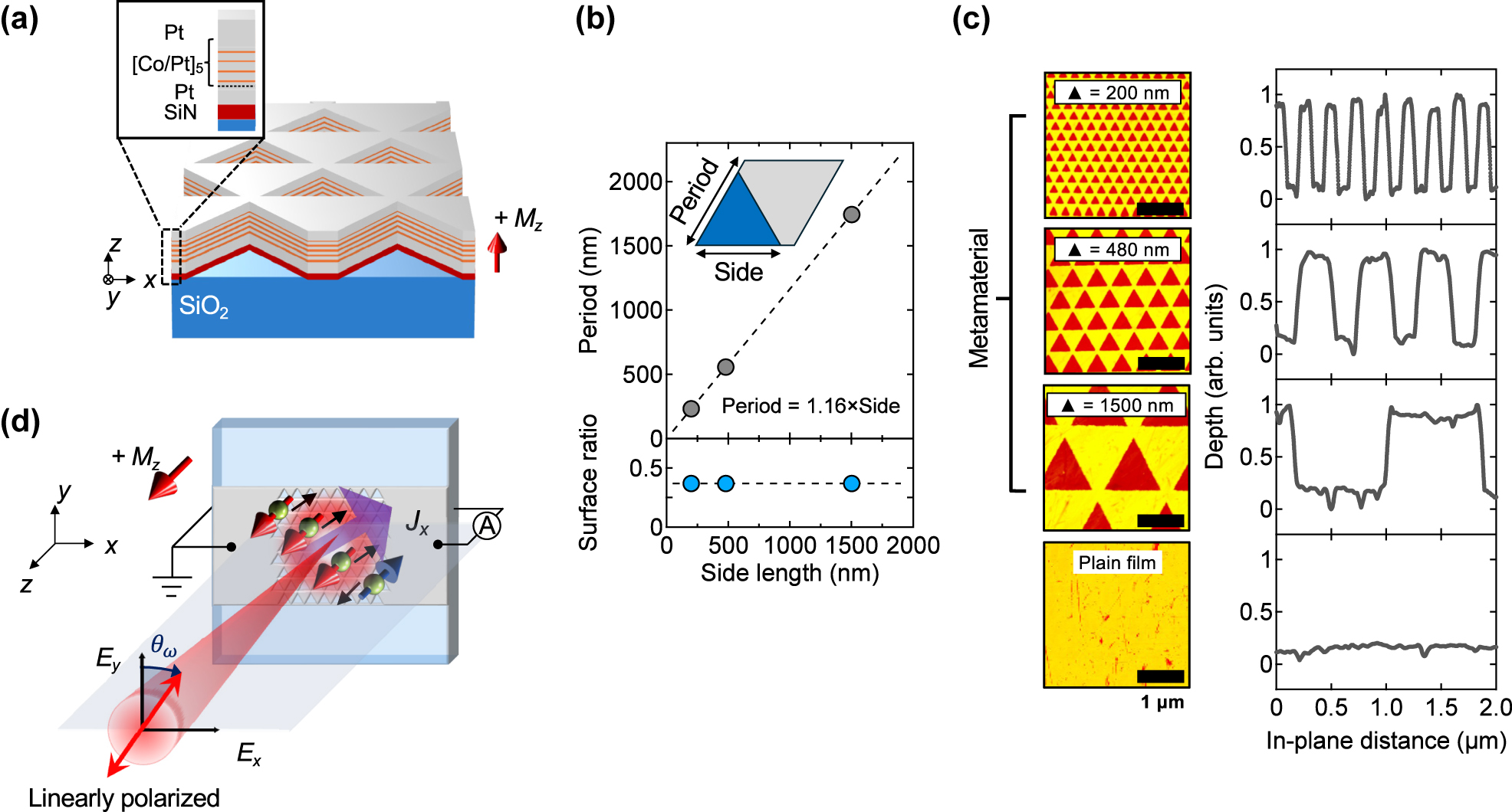
Sample design and experimental setup. (a) Schematic of a centrosymmetric Co/Pt ferromagnetic multilayer with out-of-plane magnetization M z , patterned into a triangular-hole lattice. The inset illustrates the multilayer structure (see Section 4 for details). (b) Definition of the MM unit cell. The lattice period scales with the side length of the triangular holes while maintaining a constant metal-fill factor across all samples. Fabricated MMs have side lengths of 200 nm, 480 nm, and 1,500 nm, corresponding to lattice periods of 233 nm, 558 nm, and 1,744 nm, respectively. (c) AFM images of the three MMs and a reference plain film (left), along with the corresponding normalized cross-sectional profiles (right), confirm the designed triangular geometry and hole structure. (d) Schematic of the experimental setup used to measure the zero-bias photocurrent J x , which varies with the polarization of the incident light.
Once the magnetic point group of the MMs is specified, the symmetry-allowed components of
Symmetry-allowed tensor components for PGE and MPGE responsible for generating zero-bias in-plane photocurrents in MMs with threefold rotational symmetry and perpendicular magnetization.
|
β
PGE ≡
|
|
β
MPGE ≡
|
In metamaterials, the characteristic size of the nanostructure is typically smaller than the wavelength of light. To systematically examine this regime, we fabricated MMs with triangular patterns with side lengths 200, 480, and 1,500 nm (Figure 1(b)). Each triangle resides within a unit cell whose period scales with the side length, thereby keeping the metal-fill factor constant across all samples. This design ensures equivalent illumination conditions. Atomic force microscope (AFM) images confirm the intended geometry of the holes (Figure 1(c)).
Figure 1(d) illustrates the experimental setup. Under linearly polarized excitation, a photocurrent along the x direction is detected. Due to the exchange-split band structure of Co/Pt multilayer, conduction electrons are intrinsically spin-imbalanced, exhibiting a spin polarization of about 50 % near the Fermi level [25]. As a result, spin-polarized photocurrents are generated in the patterned area upon illumination. However, in Co and Pt, the spin diffusion length is several orders of magnitude shorter (a few nanometers) than the electrode separation (hundreds of micrometers), resulting in only charge currents being detectable at the contacts. Thus, in our discussion, the term “spin-polarized photocurrents” refers to the nature of the generation mechanism rather than the spin properties of the carriers at the electrodes.
Finally, by expressing the incident electric field as E = E 0(sinθ ω , cosθ ω , 0), the photocurrent is written as
clearly demonstrating the separation of PGE and MPGE through their distinct polarization dependencies.
2.3 Magnetic characterization
Nanoscale patterning of the Co/Pt multilayer suppresses domain nucleation and expansion, thereby modifying the plain film’s magnetic properties [26], [27]. To investigate this effect, we performed magneto-optical Kerr effect (MOKE) measurements in polar geometry (Figure 2(a)).
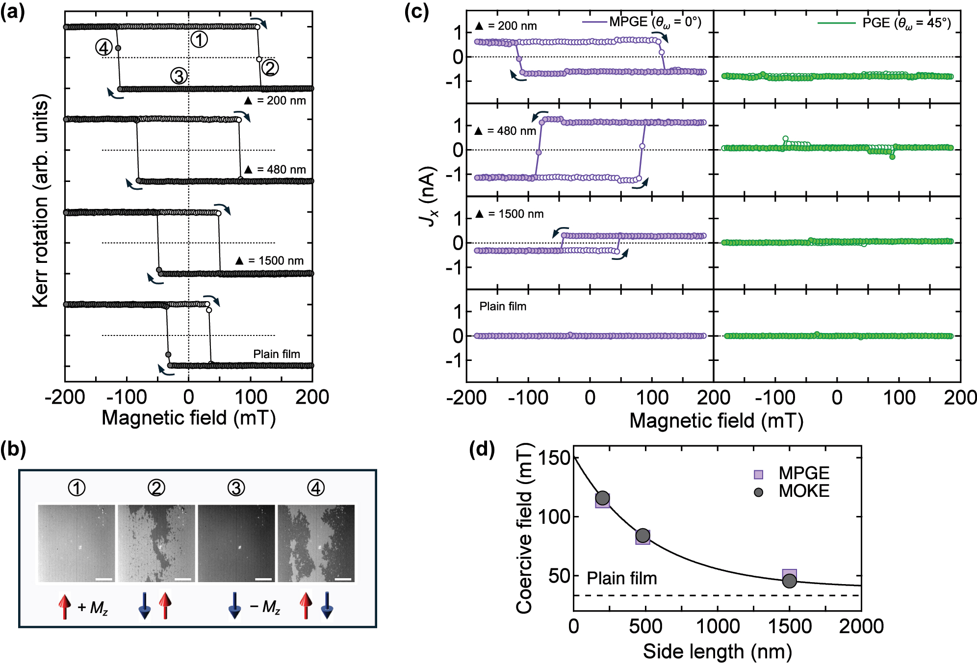
Magnetic characterization and photocurrent response of Co/Pt magnetic metamaterials. (a) Polar MOKE measurements show that the coercive field strongly depends on the nanostructure size, being largest for the 200 nm MM and smallest for the 1,500 nm MM, while all samples retain ferromagnetic behavior. (b) Representative magnetic domain images of the 200 nm MM (scale bar: 50 μm). Opposite domains appear only near the coercive field, whereas at zero field, the sample is in a single-domain state – the condition under which spin-polarized photocurrents were generated. Bright and dark contrasts correspond to up and down magnetizations, respectively. The bright dot at the center is a nonmagnetic defect on the surface. (c) Zero-bias photocurrent J x as a function of external magnetic field for MPGE (left) and PGE (right), measured at normal incidence with linearly polarized 880 nm light. MPGE shows a strong field dependence, while the PGE contribution is essentially field-independent. No photocurrent is observed in the centrosymmetric plain film. (d) Comparison of coercive fields extracted from MOKE (closed circles) and MPGE (closed squares) measurements. Coercivity in MMs approaches that of the plain film (dotted line) as hole size increases; the line is a guide to the eye.
The MOKE results reveal a systematic increase in coercivity as pattern size decreases. Compared to the unpatterned film, the coercive field of the 200 nm MM is nearly four times higher, while maintaining clear ferromagnetic behavior. Figure 2(b) shows snapshots of the saturated state and the formation of magnetic domains in the 200 nm MM, confirming complete saturation in both magnetization directions at zero field. Similar saturated and transitional states were observed across all samples. The observed coercivity enhancement in triangular holes (antidots) arrays is consistent with prior studies attributing magnetic hardening to edge-induced domain pinning, shape anisotropy, and configurational effects arising from antidot geometry and lattice symmetry, as established through micromagnetic simulations and experimental observations [28], [29].
Because of its magnetic origin, MPGE can in principle serve as an electrical probe of magnetic hysteresis. According to Eq. (3), the MPGE contribution is isolated at θ ω = 0° (left panels in Figure 2(c)), while the PGE contribution is detected at θ ω = 45° (right panels in Figure 2(c)). Under 880 nm irradiation, the hysteresis loop of the 200 nm MM inverts relative to that of larger-period MMs, suggesting that the sign of the spin-polarized photocurrent depends on nanostructure size. Nevertheless, ferromagnetic hysteresis is clearly observed in all samples (see Appendix for details on the two-step features near coercive fields). By contrast, the centrosymmetric film shows no response, consistent with the absence of MPGE or PGE.
Notably, coercive fields extracted from MOKE and MPGE measurements are in excellent agreement (Figure 2(d)). As the triangular-hole size decreases, domain expansion is progressively hindered, resulting in higher switching fields. These findings establish MPGE as a reliable electrical probe of ferromagnetic hysteresis, offering an alternative optical approach to investigate noncentrosymmetric magnets.
2.4 Polarization dependence of MPGE and PGE
Magnetic characterization of the MMs already suggested the coexistence of MPGE and PGE at certain polarization angles. To further verify the relation in Eq. (3), we systematically examined the full polarization-angle dependence of the zero-bias photocurrent at 880 nm in all samples (left panels in Figure 3). Prior to measurement, we saturated each sample in both magnetization directions and then measured photocurrents at zero external field.
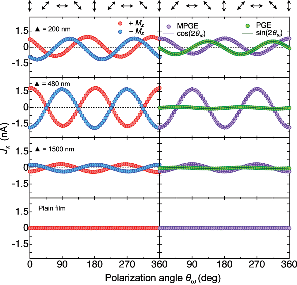
Polarization dependence of MPGE and PGE at 880 nm. The zero-bias photocurrent J x shows a clear dependence on the polarization angle θ ω of the incident light, consistent with symmetry predictions. In all MMs except the 200 nm one, the photocurrents at opposite magnetization directions are nearly equal in magnitude but opposite in sign. Subtracting the signals from opposite magnetizations isolates the MPGE contribution, whereas their sum corresponds to the magnetization-independent PGE. Under 880 nm irradiation, the MPGE amplitude is comparable to or larger than that of the PGE in all MMs. As expected, no photocurrent is detected in the centrosymmetric plain film.
At arbitrary polarization angles, MPGE and PGE signals overlap: summing currents under opposite magnetizations isolates the magnetization-independent PGE contribution, while their difference isolates the pure MPGE signal (right panels in Figure 3). In the 200 nm MM, photocurrent traces at opposite magnetizations are not perfectly symmetric, indicating a significant PGE contribution. By contrast, the 480 nm and 1,500 nm MMs show nearly symmetric responses, revealing a negligible PGE. The extracted MPGE and PGE components agree well with Eq. (3) (dark violet and green lines), confirming the validity of the model. As expected, the centrosymmetric plain film shows no photocurrent at any polarization angle, since the symmetry requirements for both MPGE and PGE are not fulfilled.
2.5 Wavelength dependence of MPGE and PGE
Results at 880 nm already highlighted a strong dependence of the photocurrent on both nanostructure size and excitation wavelength. To comprehensively investigate this behavior, we measured MPGE and PGE across the 690–1,040 nm range in 2 nm increments (Figure 4(a)).
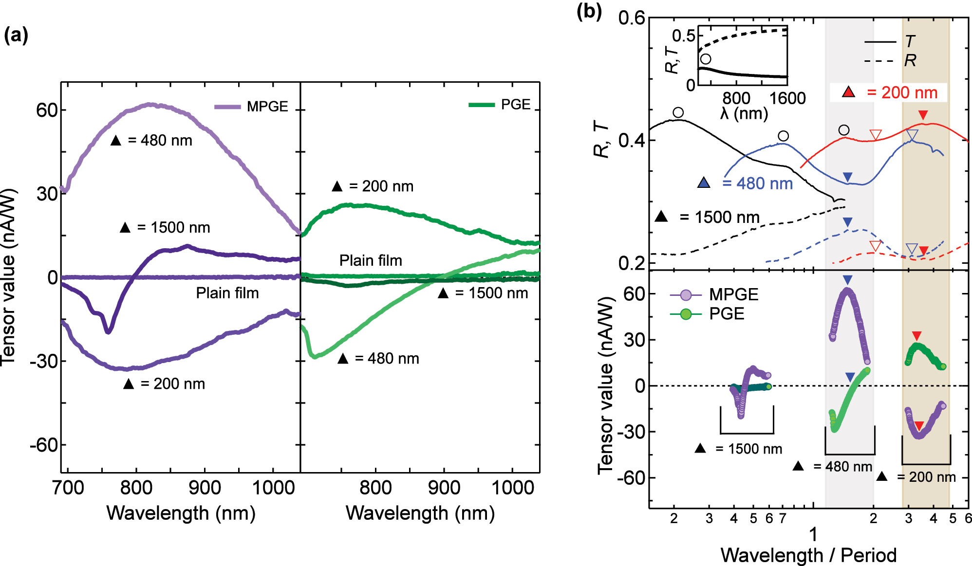
Wavelength dependence of MPGE and PGE tensors and their relation to optical spectra. (a) Dependence of β MPGE (left) and β PGE (right) on excitation wavelength for MMs with triangular side lengths of 200, 480, and 1,500 nm. In the 1,500 nm MM, MPGE vanishes near 800 nm, whereas PGE vanishes near 900 nm in the 480 nm MM. In contrast, the 200 nm MM retains both effects with opposite sign relative to the larger MMs. (b) Linear transmission (solid lines) and reflection (dotted lines) spectra normalized by lattice period (top). Corresponding normalized MPGE and PGE spectra (bottom) show that extrema and zero-crossings coincide with EOT-like features (closed triangles). Shaded areas serve as visual guides. Transmission peaks in the shorter-wavelength region (open circles) are present even in the plain film (inset), indicating that they are unrelated to the nanopatterned structure. The overlap between resonance features and photocurrent modulation highlights the key role of resonant optical coupling in tuning MPGE and PGE.
The sign and magnitude of the tensor components vary significantly among samples. For example, the MPGE of the 200 nm and 480 nm MMs remains finite but has opposite sign across the full spectral range, while the 1,500 nm MM exhibits a sign reversal around 796 nm after an initial minimum at 758 nm. This size- and wavelength-dependent inversion suggests that structural scaling can suppress MPGE even under conditions where it is symmetry-allowed. Overall, the MPGE amplitude is highest in the 480 nm MM, reaching nearly twice the level of the 200 nm MM and four times that of the 1,500 nm MM, particularly in the 750–850 nm region. The plain film yields no photocurrent across all wavelengths.
The PGE also shows complex spectral evolution. In the 480 nm MM, it develops a minimum at 710 nm, vanishes near 900 nm, and reverses sign at longer wavelengths. In the 200 nm MM, the PGE intensity is comparable to that of the 480 nm MM at shorter wavelengths but retains opposite sign relative to the larger structures. Importantly, MPGE and PGE never vanish simultaneously, and the absolute MPGE value is consistently equal to or larger than the corresponding PGE at any wavelength. These features cannot be explained solely by simple asymmetric scattering models [21], requiring further insight on the optical properties of the MMs.
2.6 Extraordinary optical transmission and resonance coupling
To clarify the role of optical resonances, we compared the photocurrent spectra with the linear transmission and reflection spectra normalized by the lattice period (Figure 4(b)). In the 200 nm and 480 nm MMs, transmission dips coincide with reflection peaks (closed and open triangles), characteristic of EOT reported in both plasmonic and lossy metals [30], [31]. In the 1,500 nm MM, however, EOT-like features are not clearly observed within the measured spectral range, suggesting that its resonance may be either weaker or shifted outside the measurement window. All samples, including the centrosymmetric reference film, exhibit a transmission peak at shorter wavelengths (open circles), attributable to the intrinsic property of the Co/Pt multilayer rather than nanopatterning.
The extrema and zero-crossings of the photocurrent spectra frequently align with these optical resonances. In the 480 nm MM, the EOT dip (blue closed triangles) coincides with a maximum in MPGE and a vanishing PGE, consistent with earlier predictions for subwavelength hole arrays [15]. In the 200 nm MM, by contrast, both PGE and MPGE peak at the EOT maximum (red closed triangles), underscoring the role of plasmon-enhanced near-fields. These fields are strongly localized at the triangular edges and vertices, where steep electric-field gradients form [32]. Such localized fields may enhance both PGE and MPGE, contributing to the spectral profiles observed across the three lattice periods. These observations suggest that resonant optical modes could play an important role in generating spin-polarized photocurrents in MMs.
In particular, the interplay of field enhancements and symmetry breaking represents a promising framework that could benefit from further theoretical modeling to establish a more complete understanding. Existing studies of this type have so far been limited to crystalline materials with atomic-scale unit cells, such as CrI3 [23], [33] and MnBi2Te4 [34], which differ by many orders of magnitude from the artificial-symmetry unit cells of our MMs. Thus, scaling-dependent MM systems represent a promising platform for both experimental and theoretical investigations.
3 Conclusions
We have demonstrated that spin-polarized photocurrents can be effectively tuned by scaling the hole size in perpendicularly magnetized Co/Pt MMs. Whereas plain films do not generate photocurrents, the triangular-hole lattices consistently produce spin-polarized photocurrents. Moreover, MPGE proved to be a powerful electrical probe of magnetism in noncentrosymmetric magnets. By systematically varying the excitation wavelength, we found that both the magnitude and the sign of photocurrents exhibit nontrivial dependence on the nanostructure size (lattice period). Importantly, MPGE and PGE never vanish simultaneously, and the MPGE amplitude consistently exceeds that of the PGE. These results highlight that nanoscale scaling governs not only the efficiency but also the polarity of photocurrent generation. Furthermore, the observed coupling between resonant optical modes and photocurrent generation points to a possible relationship between EOT and plasmonic enhancement in tailoring spin-polarized photocurrents in MMs.
Taken together, our findings establish nanoscale hole patterning as a versatile route to realizing spin-current sources that are noncontact, polarization-tunable, and wavelength-sensitive. Future efforts should focus on elucidating the underlying dynamics through advanced electromagnetic simulations and near-field optical microscopy, as well as extending PGE and MPGE studies across a broader class of materials. Such approaches hold promise for optimizing metamaterial designs and unlocking new functionalities in ultrafast spintronics and opto-spintronic devices.
4 Methods
Fabrication of magnetic metamaterials: To satisfy the symmetry conditions required for observing both PGE and MPGE, we designed MMs that simultaneously break
We fabricated four samples: three MMs with triangular side lengths of 200 nm, 480 nm, and 1,500 nm (corresponding to lattice periods of 233 nm, 558 nm, and 1,744 nm, respectively), and one unpatterned plain film used as a control. AFM images confirmed the intended geometry and high structural quality of all fabricated samples. The triangular unit cell belongs to the 3m point group with threefold symmetry. At room temperature, the Co/Pt multilayer exhibits perpendicular magnetization, preserving threefold rotational symmetry while breaking
Magneto-optical Kerr effect measurements: The response of each MM to an external magnetic field was characterized using a MOKE microscope in polar geometry. The nanoscale patterning of the MMs modifies domain nucleation and growth, resulting in an enhanced coercive field that increases as the triangular hole size decreases.
Photocurrent measurements: Using the surrounding unstructured Co/Pt film as electrodes, we measured short-circuit photocurrents in both the MMs and the plain film. All measurements were performed at room temperature under ambient conditions and at normal incidence. Excitation was provided by a tunable Ti:sapphire laser (Spectra-Physics, Mai Tai HP) operating from 690 to 1,040 nm, delivering 100 fs pulses at 80 MHz. A rotatable half-wave plate controlled the polarization angle θ ω of the linearly polarized incident light (Figure 1(d)), and the beam was focused to a ∼250 μm spot to illuminate the nanostructured region. The beam intensity was modulated at f ∼ 1 kHz with a mechanical chopper, and zero-bias photocurrents along the x direction were detected using a two-phase lock-in amplifier (SR865, Stanford Research Systems).
Linear optical measurements: The linear optical transmission (T) and reflection (R) spectra of the reference plain Co/Pt multilayer film and the MMs were measured in the 250–2,500 nm range using a commercial spectrometer (JASCO MSV-5700).
Funding source: Research Foundation for Opto-Science and Technology
Funding source: Tanaka Memorial Foundation
Funding source: Japan Science and Technology Agency
Award Identifier / Grant number: JPMJPR23H9, JPMJCR24R5
Funding source: Research Foundation for the Electrotechnology of Chubu
Funding source: Asahi Glass Foundation
Funding source: Murata Science and Education Foundation
Funding source: Mayekawa Houonkai Foundation
Funding source: TIA-Kakehashi
Award Identifier / Grant number: TK23-019, TK24-13
Funding source: TEPCO Memorial Foundation
Funding source: Japan Society for the Promotion of Science
Award Identifier / Grant number: 24H00413, 25K22081, 21H04649, 24H01639, 22K18962
Acknowledgments
MM acknowledges T. Kobayashi for his pioneering investigation of the magneto-photogalvanic effect in our magnetic metamaterials, P. Holzenkamp for his study on the size dependence of the photogalvanic effect in nonmagnetic metamaterials and for valuable discussions, Y. Ohno and Y. Nakata for their support with electromagnetic simulations. HT acknowledges support from GP-Spin at Tohoku University.
-
Research funding: This work was supported by JSPS KAKENHI (Grant Nos. 24H00413, 25K22081, 21H04649, 24H01639, 22K18962, JP23K13058, JP24K00581, and JP25H02115), JST PRESTO (Grant No. JPMJPR23H9), JST CREST (Grant No. JPMJCR24R5), the Asahi Glass Foundation, the TEPCO Memorial Foundation, TIA-Kakehashi (Grant Nos. TK23-019 and TK24-13), the Research Foundation for Opto-Science and Technology, the Support Center for Advanced Telecommunications Technology Research Foundation, the Murata Science Foundation, the Research Foundation for the Electrotechnology of Chubu, the Mayekawa Houonkai Foundation, and the Tanaka Memorial Foundation. A part of this work was conducted at the Next-generation biomaterials Hub, Nagoya University, supported by Advanced Research Infrastructure for Materials and Nanotechnology in Japan of MEXT, Japan (Grant Nos. JPMXP1222NU0226 and JPMXP1223NU0201).
-
Author contributions: MM conceived and supervised the project. GC and HT performed the photocurrent, Kerr rotation, and linear optical measurements and analyzed the data. DP, AH, DO, and TK fabricated the samples. HW provided the theoretical interpretation of the microscopic origin. GC, HT, and MM wrote the manuscript with input from HW. All authors have accepted responsibility for the entire content of this manuscript and consented to its submission to the journal, reviewed all the results and approved the final version of the manuscript.
-
Conflict of interest: Authors state no conflict of interest.
-
Data availability: The data that support the findings of this study are available from the corresponding author upon reasonable request.
Appendix: Contribution of the anomalous Nernst effect to photocurrent
In addition to MPGE and PGE, the two-step change observed in the hysteresis loop near the coercive fields – visible only in electrical measurements – can be attributed to heat-related effects at the boundary between patterned and unpatterned regions (see Figure 1(d)). We attribute this feature to the anomalous Nernst effect (ANE) [35], [36], expressed as
where E N denotes the Nernst electric field, M is the magnetization, and −∇T represents the temperature gradient across the sample. Assuming a temperature gradient along the y direction at the patterned–unpatterned boundary, an E N arises along the x direction, thereby adding to the MPGE and PGE photocurrents. This contribution becomes evident in the field interval between the coercive field of the plain film (about 33 mT) and that of each MM, where the two regions exhibit opposite magnetization along the z direction. Within this interval, the ANE contribution points in the same direction as MPGE and PGE, contributing to the total current measurement. Because the ANE scales with magnetization and unconstrained by symmetry, it manifests as a minor yet visible contributions to the overall photocurrent.
References
[1] P. Barla, V. K. Joshi, and S. Bhat, “Spintronic devices: A promising alternative to CMOS devices,” J. Comput. Electron., vol. 20, no. 2, p. 805, 2021, https://doi.org/10.1007/s10825-020-01648-6.Search in Google Scholar
[2] I. Žutić, J. Fabian, and S. Das Sarma, “Spintronics: Fundamentals and applications,” Rev. Mod. Phys., vol. 76, no. 2, p. 323, 2004, https://doi.org/10.1103/RevModPhys.76.323.Search in Google Scholar
[3] S. Maekawa, T. Kikkawa, H. Chudo, J. Ieda, and E. Saitoh, “Spin and spin current-from fundamentals to recent progress,” J. Appl. Phys., vol. 133, no. 2, p. 02092, 2022, https://doi.org/10.1063/5.0133335.Search in Google Scholar
[4] E. Beaurepaire, J. Merle, A. Daunois, and J. Bigot, “Ultrafast spin dynamics in ferromagnetic nickel,” Phys. Rev. Lett., vol. 76, no. 22, p. 4250, 1996, https://doi.org/10.1103/PhysRevLett.76.4250.Search in Google Scholar PubMed
[5] H. Zhao, E. J. Loren, H. M. van Driel, and A. L. Smirl, “Coherence control of hall charge and spin currents,” Phys. Rev. Lett., vol. 96, no. 24, p. 246601, 2006, https://doi.org/10.1103/PhysRevLett.96.246601.Search in Google Scholar PubMed
[6] M. Lalieu, R. Lavrijsen, and B. Koopmans, “Integrating all-optical switching with spintronics,” Nat. Commun., vol. 10, p. 110, 2019, https://doi.org/10.1038/s41467-018-08062-4.Search in Google Scholar PubMed PubMed Central
[7] M. Matsubara, T. Kobayashi, H. Watanabe, Y. Yanase, S. Iwata, and T. Kato, “Polarization-controlled tunable directional spin-driven photocurrents in a magnetic metamaterial with threefold rotational symmetry,” Nat. Commun., vol. 13, no. 1, p. 6708, 2022, https://doi.org/10.1038/s41467-022-34374-7.Search in Google Scholar PubMed PubMed Central
[8] M. Hild et al.., “Terahertz spin ratchet effect in magnetic metamaterials,” Phys. Rev. B, vol. 107, no. 15, p. 155419, 2023, https://doi.org/10.1103/PhysRevB.107.155419.Search in Google Scholar
[9] L. Martín-Moreno et al.., “Theory of extraordinary optical transmission through subwavelength hole arrays,” Phys. Rev. Lett., vol. 86, no. 6, p. 1114, 2001, https://doi.org/10.1103/PhysRevLett.86.1114.Search in Google Scholar PubMed
[10] S. G. Rodrigo, F. de Leon-Perez, and L. Martin-Moreno, “Extraordinary optical transmission: Fundamentals and applications,” Proc. IEEE, vol. 104, no. 12, p. 2288, 2016, https://doi.org/10.1109/jproc.2016.2580664.Search in Google Scholar
[11] H. A. Bethe, “Theory of diffraction by small holes,” Phys. Rev. Lett., vol. 66, nos. 7–8, p. 163, 1944, https://doi.org/10.1103/physrev.66.163.Search in Google Scholar
[12] T. W. Ebbesen, H. J. Lezec, H. F. Ghaemi, T. Thio, and P. A. Wolff, “Extraordinary optical transmission through sub-wavelength hole arrays,” Nature, vol. 391, no. 6668, p. 667, 1998, https://doi.org/10.1038/35570.Search in Google Scholar
[13] K. L. van der Molen, F. B. Segerink, N. F. van Hulst, and L. Kuipers, “Influence of hole size on the extraordinary transmission through subwavelength hole arrays,” Appl. Phys. Lett., vol. 85, no. 19, p. 4316, 2004, https://doi.org/10.1063/1.1815379.Search in Google Scholar
[14] J.-Y. Li, Y.-L. Hua, J.-X. Fu, and Z.-Y. Li, “Influence of hole geometry and lattice constant on extraordinary optical transmission through subwavelength hole arrays in metal films,” J. Appl. Phys., vol. 107, no. 7, p. 073101, 2010, https://doi.org/10.1063/1.3327217.Search in Google Scholar
[15] S. G. Rodrigo, V. Laliena, and L. Martín-Moreno, “Second-harmonic generation from metallic arrays of rectangular holes,” J. Opt. Soc. Am. B, vol. 32, no. 1, p. 15, 2015, https://doi.org/10.1364/JOSAB.32.000015.Search in Google Scholar
[16] D. Sekine, Y. Sato, and M. Matsubara, “Nonlinear optical detection of mesoscopic magnetic toroidal dipoles,” Appl. Phys. Lett., vol. 120, no. 16, p. 162405, 2022, https://doi.org/10.1063/5.0089235.Search in Google Scholar
[17] J. Lee et al.., “Extraordinary optical transmission and second harmonic generation in sub-10-nm plasmonic coaxial aperture,” Nanophotonics, vol. 9, no. 10, p. 3295, 2020, https://doi.org/10.1515/nanoph-2020-0066.Search in Google Scholar
[18] T. Xu, X. Jiao, G.-P. Zhang, and S. Blair, “Second-harmonic emission from sub-wavelength apertures: Effects of aperture symmetry and lattice arrangement,” Opt. Express, vol. 15, no. 21, p. 13894, 2007, https://doi.org/10.1364/oe.15.013894.Search in Google Scholar PubMed
[19] P. Schön et al.., “Enhanced second-harmonic generation from individual metallic nanoapertures,” Opt. Lett., vol. 35, no. 23, p. 4063, 2010, https://doi.org/10.1364/OL.35.004063.Search in Google Scholar PubMed
[20] A. Salomon, M. Zielinski, R. Kolkowski, J. Zyss, and Y. Prior, “Size and shape resonances in second harmonic generation from silver nanocavities,” J. Phys. Chem. C, vol. 117, no. 43, p. 22377, 2013, https://doi.org/10.1021/jp403010q.Search in Google Scholar
[21] B. I. Sturman and V. M. Fridkin, Photovoltaic and Photo-Refractive Effects in Noncentrosymmetric Materials, 1st ed., London:Routledge, 1992.Search in Google Scholar
[22] V. V. Bel’kov et al.., “Magneto-gyrotropic photogalvanic effects in semiconductor quantum wells,” J. Phys.: Condens. Matter, vol. 17, no. 21, pp. 3405–3428, 2005, https://doi.org/10.1088/0953-8984/17/21/032.Search in Google Scholar
[23] Y. Zhang et al.., “Switchable magnetic bulk photovoltaic effect in the two-dimensional magnet CrI3,” Nat. Commun., vol. 10, no. 1, p. 3783, 2019, https://doi.org/10.1038/s41467-019-11832-3.Search in Google Scholar PubMed PubMed Central
[24] R. R. Birss, Symmetry and Magnetism, 1st ed. Amsterdam, The Netherlands, North-Holland Publishing Company, 1964.Search in Google Scholar
[25] A. Rajanikanth, S. Kasai, N. Ohshima, and K. Hono, “Spin polarization of currents in Co/Pt multilayer and Co–Pt alloy thin films,” Appl. Phys. Lett., vol. 97, no. 2, p. 022505, 2010, https://doi.org/10.1063/1.3460910.Search in Google Scholar
[26] M. T. Rahman, N. N. Shams, C. H. Lai, J. Fidler, and D. Suess, “Co/Pt perpendicular antidot arrays with engineered feature size and magnetic properties fabricated on anodic aluminum oxide templates,” Phys. Rev. B, vol. 81, no. 1, p. 014418, 2010, https://doi.org/10.1103/PhysRevB.81.014418.Search in Google Scholar
[27] M. Krupinski et al.., “Magnetic transition from dot to antidot regime in large area Co/Pd nanopatterned arrays with perpendicular magnetization,” Nanotechnology, vol. 28, no. 8, p. 085302, 2017, https://doi.org/10.1088/1361-6528/aa5656.Search in Google Scholar PubMed
[28] E. Saavedra, R. M. Corona, N. Vidal-Silva, J. L. Palma, D. Altbir, and J. Escrig, “Dynamic and static properties of stadium-shaped antidot arrays,” Sci. Rep., vol. 10, no. 1, p. 20024, 2020, https://doi.org/10.1038/s41598-020-77074-2.Search in Google Scholar PubMed PubMed Central
[29] S. Mallick, S. S. Mishra, and S. Bedanta, “Relaxation dynamics in magnetic antidot lattice arrays of Co/Pt with perpendicular anisotropy,” Sci. Rep., vol. 8, no. 1, p. 11648, 2018, https://doi.org/10.1038/s41598-018-29903-8.Search in Google Scholar PubMed PubMed Central
[30] F. Przybilla, A. Degiron, J.-Y. Laluet, C. Genet, and T. W. Ebbesen, “Optical transmission in perforated noble and transition metal films,” J. Opt. Pure Appl. Opt., vol. 8, no. 5, p. 458, 2006, https://doi.org/10.1088/1464-4258/8/5/015.Search in Google Scholar
[31] S. G. Rodrigo, F. J. García-Vidal, and L. Martín-Moreno, “Influence of material properties on extraordinary optical transmission through hole arrays,” Phys. Rev. B, vol. 77, no. 7, p. 075401, 2008, https://doi.org/10.1103/PhysRevB.77.075401.Search in Google Scholar
[32] H. Lee, C. Kim, and D. Kim, “Sub-10 nm near-field localization by plasmonic metal nanoaperture arrays with ultrashort light pulses,” Sci. Rep., vol. 5, no. 1, p. 17584, 2015, https://doi.org/10.1038/srep17584.Search in Google Scholar PubMed PubMed Central
[33] C. Zhang, H. Pi, and J. Zhou, “Bulk photovoltaic effects in helimagnets,” Phys. Rev. B, vol. 110, no. 4, p. L041104, 2024. https://doi.org/10.1103/PhysRevB.110.L041104.Search in Google Scholar
[34] H. Wang and X. Qian, “Electrically and magnetically switchable nonlinear photocurrent in PT-symmetric magnetic topological quantum materials,” npj Comput. Mater., vol. 6, no. 1, p. 199, 2020, https://doi.org/10.1038/s41524-020-00462-9.Search in Google Scholar
[35] W. L. Lee, S. Watauchi, V. L. Miller, R. J. Cava, and N. P. Ong, “Anomalous Hall heat current and Nernst effect in the CuCr2Se4−xBrx ferromagnet,” Phys. Rev. Lett., vol. 93, no. 22, p. 226601, 2004, https://doi.org/10.1103/PhysRevLett.93.226601.Search in Google Scholar PubMed
[36] M. Weiler et al.., “Local charge and spin currents in magnetothermal landscapes,” Phys. Rev. Lett., vol. 108, no. 10, p. 106602, 2012, https://doi.org/10.1103/PhysRevLett.108.106602.Search in Google Scholar PubMed
© 2025 the author(s), published by De Gruyter, Berlin/Boston
This work is licensed under the Creative Commons Attribution 4.0 International License.
Articles in the same Issue
- Frontmatter
- Reviews
- Light-driven micro/nanobots
- Tunable BIC metamaterials with Dirac semimetals
- Large-scale silicon photonics switches for AI/ML interconnections based on a 300-mm CMOS pilot line
- Perspective
- Density-functional tight binding meets Maxwell: unraveling the mysteries of (strong) light–matter coupling efficiently
- Letters
- Broadband on-chip spectral sensing via directly integrated narrowband plasmonic filters for computational multispectral imaging
- Sub-100 nm manipulation of blue light over a large field of view using Si nanolens array
- Tunable bound states in the continuum through hybridization of 1D and 2D metasurfaces
- Integrated array of coupled exciton–polariton condensates
- Disentangling the absorption lineshape of methylene blue for nanocavity strong coupling
- Research Articles
- Demonstration of multiple-wavelength-band photonic integrated circuits using a silicon and silicon nitride 2.5D integration method
- Inverse-designed gyrotropic scatterers for non-reciprocal analog computing
- Highly sensitive broadband photodetector based on PtSe2 photothermal effect and fiber harmonic Vernier effect
- Online training and pruning of multi-wavelength photonic neural networks
- Robust transport of high-speed data in a topological valley Hall insulator
- Engineering super- and sub-radiant hybrid plasmons in a tunable graphene frame-heptamer metasurface
- Near-unity fueling light into a single plasmonic nanocavity
- Polarization-dependent gain characterization in x-cut LNOI erbium-doped waveguide amplifiers
- Intramodal stimulated Brillouin scattering in suspended AlN waveguides
- Single-shot Stokes polarimetry of plasmon-coupled single-molecule fluorescence
- Metastructure-enabled scalable multiple mode-order converters: conceptual design and demonstration in direct-access add/drop multiplexing systems
- High-sensitivity U-shaped biosensor for rabbit IgG detection based on PDA/AuNPs/PDA sandwich structure
- Deep-learning-based polarization-dependent switching metasurface in dual-band for optical communication
- A nonlocal metasurface for optical edge detection in the far-field
- Coexistence of weak and strong coupling in a photonic molecule through dissipative coupling to a quantum dot
- Mitigate the variation of energy band gap with electric field induced by quantum confinement Stark effect via a gradient quantum system for frequency-stable laser diodes
- Orthogonal canalized polaritons via coupling graphene plasmon and phonon polaritons of hBN metasurface
- Dual-polarization electromagnetic window simultaneously with extreme in-band angle-stability and out-of-band RCS reduction empowered by flip-coding metasurface
- Record-level, exceptionally broadband borophene-based absorber with near-perfect absorption: design and comparison with a graphene-based counterpart
- Generalized non-Hermitian Hamiltonian for guided resonances in photonic crystal slabs
- A 10× continuously zoomable metalens system with super-wide field of view and near-diffraction–limited resolution
- Continuously tunable broadband adiabatic coupler for programmable photonic processors
- Diffraction order-engineered polarization-dependent silicon nano-antennas metagrating for compact subtissue Mueller microscopy
- Lithography-free subwavelength metacoatings for high thermal radiation background camouflage empowered by deep neural network
- Multicolor nanoring arrays with uniform and decoupled scattering for augmented reality displays
- Permittivity-asymmetric qBIC metasurfaces for refractive index sensing
- Theory of dynamical superradiance in organic materials
- Second-harmonic generation in NbOI2-integrated silicon nitride microdisk resonators
- A comprehensive study of plasmonic mode hybridization in gold nanoparticle-over-mirror (NPoM) arrays
- Foundry-enabled wafer-scale characterization and modeling of silicon photonic DWDM links
- Rough Fabry–Perot cavity: a vastly multi-scale numerical problem
- Classification of quantum-spin-hall topological phase in 2D photonic continuous media using electromagnetic parameters
- Light-guided spectral sculpting in chiral azobenzene-doped cholesteric liquid crystals for reconfigurable narrowband unpolarized light sources
- Modelling Purcell enhancement of metasurfaces supporting quasi-bound states in the continuum
- Ultranarrow polaritonic cavities formed by one-dimensional junctions of two-dimensional in-plane heterostructures
- Bridging the scalability gap in van der Waals light guiding with high refractive index MoTe2
- Ultrafast optical modulation of vibrational strong coupling in ReCl(CO)3(2,2-bipyridine)
- Chirality-driven all-optical image differentiation
- Wafer-scale CMOS foundry silicon-on-insulator devices for integrated temporal pulse compression
- Monolithic temperature-insensitive high-Q Ta2O5 microdisk resonator
- Nanogap-enhanced terahertz suppression of superconductivity
- Large-gap cascaded Moiré metasurfaces enabling switchable bright-field and phase-contrast imaging compatible with coherent and incoherent light
- Synergistic enhancement of magneto-optical response in cobalt-based metasurfaces via plasmonic, lattice, and cavity modes
- Scalable unitary computing using time-parallelized photonic lattices
- Diffusion model-based inverse design of photonic crystals for customized refraction
- Wafer-scale integration of photonic integrated circuits and atomic vapor cells
- Optical see-through augmented reality via inverse-designed waveguide couplers
- One-dimensional dielectric grating structure for plasmonic coupling and routing
- MCP-enabled LLM for meta-optics inverse design: leveraging differentiable solver without LLM expertise
- Broadband variable beamsplitter made of a subwavelength-thick metamaterial
- Scaling-dependent tunability of spin-driven photocurrents in magnetic metamaterials
- AI-based analysis algorithm incorporating nanoscale structural variations and measurement-angle misalignment in spectroscopic ellipsometry