Scalable unitary computing using time-parallelized photonic lattices
-
Hyungchul Park

 and
Xianji Piao
and
Xianji Piao

Abstract
Exploiting alternative physical dimensions beyond the spatial domain has been intensively explored to improve the scalability in photonic computing. One approach leverages dynamical systems for time-domain computation, enabling universal and reconfigurable unitary operations. Although this method yields O(N) scaling in both device footprint and gate count, the required computation time increases by O(N 2), which hinders practical implementation due to limitations in quality factors and modulation speeds of optical elements. Here, we propose time-parallelized photonic lattices that achieve O(N) time scalability while preserving the O(N) spatial scaling. We devise a pseudospinor buffer operation that temporally stores the optical information, thereby enabling parallel unitary computation. The proposed method not only mitigates the requirement for high-quality factors but also provides robustness against a broad range of defects, demonstrating the feasibility of time-domain photonic computation.
1 Introduction
Parallelism is at the heart of modern computing technologies, as shown in graphic processing units to achieve improved scaling of computational speed [1], [2]. In implementing parallel computing, a fundamental requirement is to realize synchronization over multiple signal flows, which enables coordinated operations of processing units when executing specific tasks. Synchronization in electronic computing is achieved through buffer elements, such as latches and flip-flops.
To address critical limitations in programmable photonic circuits (PPCs) [3], [4], [5], [6], [7], [8], [9], [10], [11], [12] – O(N 2) scalability in device footprint and gate count [13], [14] – time-domain unitary computation using resonator lattices has been proposed, achieving O(N) spatial scalability [15], [16]. In this programmable photonic time circuit (PPTC), however, it is more challenging to enable synchronization than conventional PPCs due to different operation times between photonic gates. The resulting lack of synchronization enforces sequential rather than parallel gate operations, causing the operating time to increase by O(N 2). This scaling in the time domain requires optical elements with ultrahigh quality (Q) factors to store light throughout the computation. For example, it was expected that resonators with Q ∼ 108 would be required even for N = 10 in conventional PPTC platforms [15]. Therefore, it is urgent to devise a suitable optical buffer [17], [18], [19] that is compatible with computing circuits, overcoming the difficulty of achieving optical bistability [20], [21], [22] necessary for memory functions.
Here, we propose a parallelized PPTC that employs the buffer element of pseudospinor states to synchronize different SU(2) gates. By exploiting the temporal and spatial programmability of PPTCs, the states of light at the target sites can be buffered by decoupling neighboring resonators through destructive interferences. We apply the buffering to compensate for variations in SU(2) gate latency, enabling synchronized SU(2) operations. The proposed synchronization scheme allows for the pristine implementation of the Clements design [14] with O(N) time complexity, which substantially lowers the required Q-factor and improves robustness against defects compared to the previous scheme [15]. This result enables a practical implementation of photonic computing for both classical and quantum applications.
2 Time-parallelized lattices
2.1 Synchronized PPTCs
Implementing high-dimensional and universal unitary operations using light signals [13], [14], [23], [24], [25], [26], [27], [28] has become an urgent issue in achieving photonic deep learning acceleration [29], [30] and quantum gate operations [7], [31], [32]. Although recent studies have enabled the use of higher-dimensional units for more compact design [23], [24], [25], [26], [27], [28], the most conventional approach for analytically deterministic design procedures relies on the factorization of a matrix U N ∈ U(N) into a set of SU(2) matrices and a diagonal matrix [13], [14]. Each step of factorization is designed to achieve the nulling of an off-diagonal component, by applying a universal SU(2) operation to the unitary matrix U N . Such a nulling process continues sequentially until the matrix becomes diagonal, thereby allowing for the deterministic configuration of U N through the cascaded multiplications of physically achievable SU(2) and diagonal matrices.
The sequence of the nulling processes can be implemented in different forms, for example, by nulling the components of each row (or column) sequentially – the Reck design [13] – or by nulling from higher- to lower-order off-diagonals – the Clements design [14]. These sequences lead to distinct circuit depth, as shown in the Clements design with a half of the circuit depth compared to the Reck design. However, both approaches eventually possess O(N) scaling in the circuit depth, leading to O(N 2) scaling in the overall device footprint.
To address the scalability issue, recent studies have proposed the utilization of wave evolutions along alternative physical axes, such as frequency synthetic dimension [33], [34], [35], [36] or temporal perturbations [15], [16], [37], [38], [39], [40]. In these approaches, one popular candidate is to utilize coupled-resonator optical waveguides (CROWs) [41], [42], [43], which enable dynamical modulation of the system for temporal- [15], [16] or frequency-domain [33], [35] tailoring of optical states. In the time-domain computing approach based on the concept of PPTCs [15], [16], the unit gate consists of a pair of resonators coupled through the zero-field loop couplers [42], [43] (Figure 1a), which can be modulated with refractive index changes. While each resonator supports the clockwise and counter-clockwise resonance modes, we focus on the clockwise mode, which leads to the Hamiltonian H governing the gate dynamics [15]:
where ω 0 is the reference resonance frequency, Δω(t) is the resonance perturbation, ξ L (or ξ U) characterizes the phase shifts of the lower (or upper) loop coupler, τ is the lifetime determined by the coupling between a resonator and a loop coupler, and σ 0 and σ x,y,z are the identity matrix and Pauli matrices, respectively (Figure 1a).
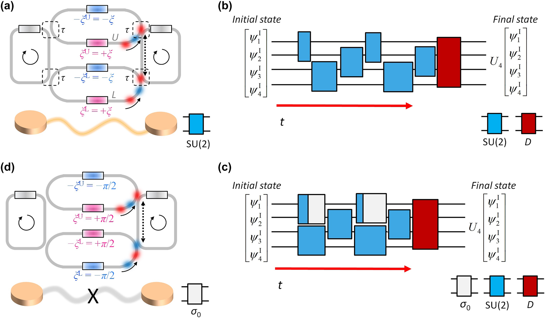
Synchronized operation of PPTC. (a) SU(2) gate composed of two resonators coupled via lower and upper loop couplers. Each loop coupler includes two phase shifters (colored boxes): ±ξ L and ±ξ U for lower and upper loop couplers, where +ξ L and +ξ U (or –ξ L and –ξ U) denote the lower (or upper) phase shifters of each coupler, respectively. Each resonator includes the phase shifter for resonance perturbation Δω(t) (gray boxes). (b,c) Universal unitary operations U N using the PPTC for N = 4: serial execution protocol (b) and parallel execution protocol using buffering (c). D ∈ U(4) denotes the designed 4-dimensional diagonal unitary matrix. (d) Buffering function achieved with the SU(2)-gate structure. In (a, d), dashed boxes and solid arrows denote the coupling regions and the direction of wave propagation, respectively. Dashed arrows represent the propagation length of an integer multiple of the effective wavelength of light.
When we set Δω(t) = 0 and ξ L = ξ U = ξ (Figure 1a), the system Hamiltonian becomes H = −ω 0 σ 0 − (1/τ)[σ x cosξ + σ y sinξ] according to Eq. (1). Therefore, the gate yields an arbitrary and reconfigurable rotation operation on the Bloch sphere about the axis n = (cosξ, sinξ, 0), where the amount of the rotation is determined by the time Δt maintaining the system parameters and the corresponding H [15]. For the modulation range of 0 ≤ ξ < 2π, the SU(2) gate operations required for decomposing arbitrary U(N) matrices are guaranteed by controlling Δt.
These gate operations serve as the building blocks for realizing universal U(N) operations. To implement a given U(N) operation, we can construct a one-dimensional (1D) resonator lattice composed of the resonators coupled via the coupler in Figure 1a, while mapping each resonator mode to a basis. For an initial resonance state [ψ 1 I, ψ 2 I, … ψ N I]T, the cascaded, designed SU(2) gate operations for pairs of resonators (blue boxes in Figure 1b) implement the target matrix U N ∈ U(N) with the final diagonal matrix (the red box in Figure 1b) that can be achieved with elementwise resonance detuning [15], [16]. We note that the SU(2) operations are executed sequentially in time [15], [16], in contrast to the spatial arrangement in the spatial PPCs [3], [4], [5], [6], [7], [8], [9], [10], [11], [12].
However, the critical hurdle of the PPTC described in [15], [16] is the poor scaling along the temporal axis, which exhibits O(N 2) scaling. This limitation originates from the operation principle of an SU(2) gate: the state rotation on the Bloch sphere of which the speed is determined by the coupling strength between resonators and loop couplers. Due to the static coupling determined by the stationary location of optical elements (dashed boxes in Figure 1a), the necessary times to achieve the target SU(2) operations are differentiated for each nulling process and the form of U N . Consequently, the temporal depths of SU(2) gates are not to be the same, leading to asynchronization and inevitably requiring sequential rather than parallel computing process (Figure 1b). The resulting O(N 2) temporal circuit depth not only degrades the operation speed but also enforces the necessity of ultrahigh Q-factor resonators to store light during the computation [15].
To resolve this poor time scaling issue, we develop the synchronization scheme for the PPTC. Figure 1c shows the proposed design protocol to resolve the time-scaling issue, by synchronizing multiple independent gate operations to the longest-latency one using the buffering functions (white boxes with 2 × 2 identity operations). This can be implemented by the odd-parity configuration with ξ U(t) = −ξ L(t) = π/2, which leads to decoupling between resonators through the system Hamiltonian H = −ω 0 σ 0 [15].
2.2 U(N) operation with buffering
To demonstrate the proposed scheme, we design the phase shifters of the PPTC under the protocol described in Figure 1c. As an example, we investigate the state evolution for a U 4 matrix. The decomposition based on the Clements design for U N [14] requires the circuit composed of (N + 1) layers: N layers for SU(2) operations and 1 diagonal-operation layer (Figure 2a). Each layer includes n (≈N/2) SU(2) gates in parallel, executing SU(2) matrices {T 1, T 2, … T n } during distinct operation times {Δt 1, Δt 2 … Δt n }. Because Δt i ≠ Δt j in general, we introduce an additional buffer duration of max(Δt 1, Δt 2 … Δt n ) − Δt i for each operation T i after completing the designed gate operation. This ensures that all gates in the set complete the operation synchronously with a common cycle period of max(Δt 1, Δt 2 … Δt n ).
![Figure 2:
Synchronized U
4 PPTC example. (a) Schematic of the PPTC and its time coded modulations: the resonance shift for the n-th resonator, Δω
n
, and the phase shifts ξ
n,(n+1)
L,U for the loop coupler between the n-th and (n+1)-th resonators [15]. Each modulation is scheduled to satisfy synchronization. Considering the device bandwidth in real implementation, an ideal set of modulation signals are then low-pass filtered with the cut-off frequency ω
c = 0.01ω
0. (b, c) Bloch-sphere representations of the pseudospinor states ψ
1,2 = [ψ
1, ψ
2]T (b) and ψ
3,4 = [ψ
3, ψ
4]T (c), which are defined by the resonance modes of the neighboring resonators 1 and 2, and 3 and 4, respectively. The Stokes parameters S
i∈x,y,z
= ψ
n,(n+1)
T
σ
i
ψ
n,(n+1) are plotted on the unit sphere. The evolutions of the states are plotted during time t
0 ≤ t ≤ t
1, where t
b denotes the completion time of the SU(2) operation between the resonators 3 and 4. Black stars denote the target states. The buffering function is observed in-between t
b (marked in purple) and t
1 (marked in red).](/document/doi/10.1515/nanoph-2025-0498/asset/graphic/j_nanoph-2025-0498_fig_002.jpg)
Synchronized U 4 PPTC example. (a) Schematic of the PPTC and its time coded modulations: the resonance shift for the n-th resonator, Δω n , and the phase shifts ξ n,(n+1) L,U for the loop coupler between the n-th and (n+1)-th resonators [15]. Each modulation is scheduled to satisfy synchronization. Considering the device bandwidth in real implementation, an ideal set of modulation signals are then low-pass filtered with the cut-off frequency ω c = 0.01ω 0. (b, c) Bloch-sphere representations of the pseudospinor states ψ 1,2 = [ψ 1, ψ 2]T (b) and ψ 3,4 = [ψ 3, ψ 4]T (c), which are defined by the resonance modes of the neighboring resonators 1 and 2, and 3 and 4, respectively. The Stokes parameters S i∈x,y,z = ψ n,(n+1) T σ i ψ n,(n+1) are plotted on the unit sphere. The evolutions of the states are plotted during time t 0 ≤ t ≤ t 1, where t b denotes the completion time of the SU(2) operation between the resonators 3 and 4. Black stars denote the target states. The buffering function is observed in-between t b (marked in purple) and t 1 (marked in red).
Figure 2a illustrates the designed temporal modulation of the phase shifters under this protocol. In cycle 1, the gate operations T 1 and T 2 are executed in parallel, leading to the required SU(2) operations for the resonator pairs (1, 2) and (3, 4), respectively. Upon completion of T 2 at time t b, the (3, 4) resonator pair is on the buffering mode, freezing the pseudospinor state without any energy exchange or the emergence of relative phase shift.
From the designed modulation, we calculate the PPTC operation following the same numerical method in [15], [16]: the application of the sixth-order Runge–Kutta (RK6) method [44] to solve the time-dependent equation idΨ/dt = HΨ with Eq. (1). The operations based on buffering are visualized on the Bloch sphere in Figure 2b and c. Because T 1 has the longest latency execution time in this cycle, the designed SU(2) operation on [ψ 1(t 0), ψ 2(t 0)]T completes at time t 1 (Figure 2b). Meanwhile, the operation T 2 completes earlier at time t b, and the state of [ψ 3(t b), ψ 4(t b)]T remains stationary on the buffer mode until t 1 (Figure 2c). As a result, the pseudospinor states of both pairs [ψ 1(t 0), ψ 2(t 0)]T and [ψ 3(t 0), ψ 4(t 0)]T reach their target output state simultaneously at t 1, demonstrating the state synchronization via buffering.
3 Results
3.1 Time scaling
To assess the impact of the proposed synchronization scheme, we evaluate the operation time T required to fully implement an arbitrary unitary matrix U N . Figure 3a presents the time scaling evaluated using 50 random Haar unitary matrices for each N [45], where the power-law fitting provides the exponent α = 2.10 for the serial scheme and α = 1.01 for the synchronization scheme. We observe an apparent improvement of time scaling from O(N 2) to O(N) under the proposed synchronization scheme, reflecting the reduction in required cycles from M = N(N – 1)/2 + 1 to M = N + 1 for U N implementation.
![Figure 3:
Time and Q-factor scaling. (a) Time scaling for N. The power-law exponents are α = 2.10 and α = 1.01 for the serial and synchronization schemes, respectively. (b) Q-factor scaling for N. In (a, b), blue and pink dots represent the 50 realizations for the serial and synchronization schemes, respectively. The colored dashed lines denote the power-law fittings of the data using the mean square error. The black dashed line in (b) corresponds to Q = 4 × 10⁷ experimentally demonstrated with the TFLN ring resonator [46]. The achievable N estimated with the fitted Q is marked as a black dot each for the serial and synchronization schemes.](/document/doi/10.1515/nanoph-2025-0498/asset/graphic/j_nanoph-2025-0498_fig_003.jpg)
Time and Q-factor scaling. (a) Time scaling for N. The power-law exponents are α = 2.10 and α = 1.01 for the serial and synchronization schemes, respectively. (b) Q-factor scaling for N. In (a, b), blue and pink dots represent the 50 realizations for the serial and synchronization schemes, respectively. The colored dashed lines denote the power-law fittings of the data using the mean square error. The black dashed line in (b) corresponds to Q = 4 × 10⁷ experimentally demonstrated with the TFLN ring resonator [46]. The achievable N estimated with the fitted Q is marked as a black dot each for the serial and synchronization schemes.
Because our time-domain computation is conducted while light is stored in the resonators, reducing the operation time directly alleviates the requirement for high-Q optical elements. In Figure 3b, we estimate a lower bound of the intrinsic Q factor of each resonator via Q = ω 0 T, where the full computation time T is obtained using the lifetime parameter τ = 10T M to ensure the conservation of sufficient optical signals during the computation. We calculate the bound for 10 GHz modulation bandwidth of T M ∼ 0.1 ns timescale, which is an accessible number with thin-film lithium niobate (TFLN) modulators [47]. The calculated Q in Figure 3b demonstrates the significant alleviation for implementing high-dimensional unitary operations under the synchronization scheme, enabling U 21 operations with the Q = 4 × 10⁷ resonators, in contrast to the U 8 limit in the prior serial scheme [15].
3.2 Fidelity analysis
Given the substantial reduction in operation time achieved with the synchronization scheme, we can reasonably expect improved operational fidelity at the same level of system defects, because shorter operation times reduce the exposure of light to defects. To examine this prediction, we evaluate various types of defects relevant to our architecture: fluctuations in the resonance frequency ω 0 and the coupling lifetime τ, the altered zero-field condition of loop couplers, and resonator radiation loss. We characterize all these defects using a uniformly random distribution unif(a, b): ω 0′ = [1 + unif(−σ, σ)]ω 0, ω 0″ = [1 + i × unif(0, 2σ)]ω 0, 1/τ′ = [1 + unif(−σ, σ)]/τ, and Δφ = unif(−σ, σ)π, where ω 0′ and ω 0″ denote the real- and complex-valued resonance frequencies accounting for resonance fluctuations and radiation loss, respectively, τ′ denotes the perturbed lifetime defined for the uniformly random perturbation of the coupling between a resonator and a loop coupler, and Δφ is the unwanted phase shift exerted on each arm of the loop couplers.
For the target unitary operation U N and its PPTC realization V N , we examine the operational fidelity with the following Frobenius-norm error:
where Tr[A] denotes the trace of matrix A. Although the error ε satisfies 0 ≤ ε ≤ 2 for the unitary output V N , this bound no longer applies to nonunitary V N . The defects characterized by the altered zero-field condition of loop couplers and resonator radiation loss lead to nonunitary V N because optical energy is transferred into the loop coupler and environment, respectively, and therefore, the resonator-system Hamiltonian is no longer Hermitian.
To estimate ε statistically, we follow the procedure in the previous work [15]. In obtaining the V N for one target U N , we calculate the PPTC operations for the N input states ψ n I (n = 1, 2, …, N), which are obtained by normalizing N × 1 complex vectors that have the amplitudes unif(0, 1) and the phases unif(0, 2π). For initial field distributions of {ψ n I} inside the PPTC, we obtain N different outputs ψ n O using the RK6 method, which allow for estimating V N directly through the following inversion, as
In evaluating ε, we examine 10 random Haar unitary matrices as the target unitary operations.
Figure 4a–d shows the σ-dependent errors for the serial and synchronized implementations at N = 5 and N = 20. Although the detailed dependencies vary with the type of defects – for example, more sensitive responses to resonance perturbations than to the lifetime variations – the synchronization scheme consistently exhibits superior robustness against defects compared to the serial implementation. Notably, such an improvement in robustness by the synchronization is evident especially in larger systems (N = 20 in Figure 4(b, d, f, h) versus N = 5 in Figure 4(a, c, e, g)). This trend also holds for other values of N as shown in Supplementary Note S1.
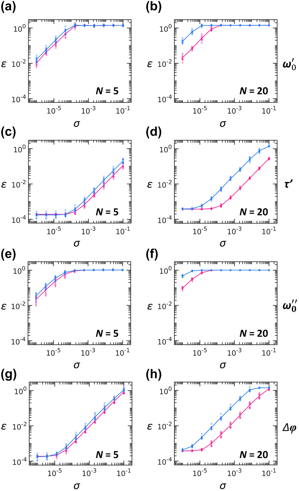
Robustness against defects. (a–d) Variations of errors with respect to the degree of defects σ: (a, b) resonance fluctuations, (c, d) lifetime fluctuations, (e, f) resonator radiation loss, and (g, h) phase-shift defects in loop couplers. Blue and pink dots denote ε obtained with 10 realizations of random Haar matrices at each value of σ. Solid lines denote their averages. We compare the serial (blue) and synchronization (pink) scheme for small- (N = 5) and large-scale (N = 20) systems for each type of defects.
3.3 Analysis for real implementation
We evaluate the computing performance of our PPTCs in terms of real implementation, including the comparisons with the prior serial configuration [15], [16] and with other electronic [48] and photonic [29] platforms. Our target calculation – U N matrix multiplication to an N × 1 vector – includes N 2 multiplications and N(N − 1) additions of complex scalars. Because a multiplication and an addition of complex scalars require six and two operations regarding real-valued scalar calculations, respectively, the target calculation requires 8N 2 – 2N real-valued operations.
The operation times of the PPTCs are governed by the SU(2) gate operation time, which is comparable to τ. Because the time scalabilities of the serial [15], [16] and our synchronized implementations are O(N 2) and O(N), respectively (Figure 3), the operations (OPs) per second (OPS) of PPTC become ≈ (8N 2 – 2N)/(N 2 τ) ≈ 8/τ OPS in the serial design [15], [16] and ≈ (8N 2 – 2N)/(Nτ) ≈ 8N/τ OPS for our design. This estimation demonstrates that the parallelization enables scalable photonic computing with the operation speed proportional to the system size N. To reach the cutting-edge electronic GPU performance close to 103 tera-OPS (TOPS) [48], the synchronized PPTC requires N/τ ≈ 1014, which can be achieved with 104 resonators under ultrafast electro-optic modulation (τ ≈ 0.1 ns, [47], [49], [50]). Considering the difficulty of achieving the stable coupling of a huge number of resonators, the application of systolic matrix multiplications [51], [52], [53] can be a candidate using a lattice of about 102 coupled resonators.
We also estimate energy efficiency, by assuming the modulator in [49], which supports 0.63 mW power consumption and 5 mm2 footprints. According to its O(N) scaling of the gate number, the PPTCs support ≈ 8,000/(Nτ) OP/J with the serial process [15], [16] and ≈ 8,000/τ OP/J with the synchronization design. Notably, our scheme using ultrafast electro-optic modulation surpasses the energy efficiency of the cutting-edge electronic GPU that supports a few TOP/J.
In terms of substituting the spatial axis with temporal axis, we further examine a comparison with the spatial PPCs [29]. We note that PPCs provide superior operation-speed scalability with ≈ (8N 2 – 2N)/τ D OPS and comparable power efficiency ≈ 8,000/τ D OP/J, where τ D is the characteristic time of photodetection and the power efficiency is governed by the O(N 2) phase-shift bias power for large N. When assuming τ D = 0.1 ns detection time, the PPC achieves 10 TOPS and 100 TOP/J with N ≈ 10, which leads to the footprint of 500 mm2 – comparable to the cutting-edge GPU die size of 103 mm2. However, the PPC suffers from poor scalabilities in the footprint and gate number, leading to 5 × 104 mm2 footprint and 104 phase shifters for N ≈ 100, hindering the increase of computing dimension despite superior operation speed of 103 TOPS. Therefore, the major advantage of the PPTC lies in the scalability of the gate number and footprint: 500 mm2 footprint and ∼500 phase shifters for N ≈ 100.
We note that the spatio-temporal computing circuit composed of waveguides and resonators, which has been very recently studied for the different purpose [54], [55] – nonlinear expressivity in photonic deep learning – would be a candidate platform resolving both the dimensionality limit of PPCs and the speed limit of PPTCs. This configuration also maintains the potential advantage of PPTCs as all-optical programmable devices – the use of resonance modes for energy localization and the consequent enhanced nonlinearity – which has been partly examined in [54], [55].
4 Conclusions
In conclusion, we proposed a synchronization scheme for the time-parallel assembly of gates in designing PPTC, enabled by a buffering function. Our analysis shows that the synchronization scheme reduces the temporal complexity from O(N 2) to O(N) while maintaining spatial efficiency. The resulting reduction in operation time significantly lowers the required resonator Q-factor, mitigating a critical hurdle for practical implementation of time-domain computation. We further explored the fidelity issue by comparing the serial and synchronized implementations, demonstrating that the proposed parallelization enhances robustness against various types of defects that are unavoidable in real fabrication processes.
Although we investigated the scalability of PPTCs based on the parallelization scheme, further issues, such as the input–output configuration [42], [43], physical origins of noises, and the synchronization of electro-optic modulation, need to be addressed for practical implementation. First, to excite and read out the signals with the PPTC platforms, one may consider the coupling of a probe waveguide to each resonator. In this case, there is a tradeoff relationship between the signal level and operation speed restricted by the ratio between the waveguide-resonator coupling Q-factor and the inter-resonator coupling Q-factor [15]. Therefore, our parallelization scheme, which substantially mitigates the restriction on the inter-resonator coupling Q-factor that must be much smaller than the intrinsic Q-factor of each resonator, extends the design space of system parameters for real implementation.
Second, while we examined the robustness of the system for the static form of defects, such as fabrication errors, possible major origins of the noise include the thermal crosstalk between optical components, which originates from dynamical modulation in phase shifters. In dense resonator meshes, the heat generated by one actuator perturbs the phase of many neighboring elements, leading to correlated phase errors [56], [57], [58], [59]. Although the parallel operation in our work may mitigate the influence of such a correlated noise in a statistical manner due to global change of refractive index over the entire system, this effect should be problem-specific and requires a further study based on multiphysics modeling [60].
Finally, when electro-optical modulation is incorporated into our PPTC design, time-varying voltage signals must be delivered to each phase shifter nearly simultaneously on a time scale much shorter than τ. Achieving this requires sub-nanosecond synchronization of the electrical signals, which can be realized using synchronized digital-to-analog converters together with delay precalibration [49]. However, when considering the accumulation of errors throughout the entire circuit, developing appropriate error-correction schemes [61], [62], [63], [64], [65] for our time-domain computation will become another critical research direction.
Our results establish a scalable and robust platform for high-dimensional photonic unitary operations, advancing toward the practical implementation of photonic computing and classical emulation of quantum phenomena. When considering recent efforts to increase the dimensionality of unit elements for more compact and scalable design of spatial PPCs [24], [25], [26], [27], [28], we can envisage further enhancement of scalability using two-dimensional lattice configuration of PPTCs with advanced parallelization schemes. The extension of the demonstrated scalable unitary operations to nonlinear functionalities [54], [55], [66], [67] would also be a future challenge.
Funding source: National Research Foundation of Korea
Award Identifier / Grant number: RS-2024-00397664
Award Identifier / Grant number: RS-2025-00552989
Funding source: Korea Basic Science Institute
Award Identifier / Grant number: RS-2024-00398604
-
Research funding: This work was supported by the National Research Foundation of Korea (NRF) grants funded by the Korea government (MSIT): the Young Researcher Program (No. RS-2025-00552989) and Basic Research Laboratory (No. RS-2024-00397664). The work was also supported by Korea Basic Science Institute (National research Facilities and Equipment Center) grant funded by the Ministry of Science and ICT (No. RS-2024-00398604) and Creative-Pioneering Researchers Program through Seoul National University.
-
Author contributions: HP, SY, and XP conceived the idea. HP developed the theoretical tool and performed the numerical analysis. BC and HJ examined the theoretical and numerical analysis. SY and XP supervised the findings of this work. All authors have accepted responsibility for the entire content of this manuscript and consented to its submission to the journal, reviewed all the results, and approved the final version of the manuscript.
-
Conflicts of interest: Authors state no conflicts of interest.
-
Data availability: The data that support the plots and other findings of this study are available from the corresponding authors upon request.
References
[1] D. B. Kirk and W. H. Wen-Mei, Programming Massively Parallel Processors, Burlington, Morgan Kaufmann, 2016.Search in Google Scholar
[2] J. Nickolls and W. J. Dally, “The GPU computing era,” IEEE Micro, vol. 30, no. 2, pp. 56–69, 2010. https://doi.org/10.1109/mm.2010.41.Search in Google Scholar
[3] W. Bogaerts, et al.., “Programmable photonic circuits,” Nature, vol. 586, no. 7828, pp. 207–216, 2020. https://doi.org/10.1038/s41586-020-2764-0.Search in Google Scholar PubMed
[4] N. C. Harris, et al.., “Linear programmable nanophotonic processors,” Optica, vol. 5, no. 12, pp. 1623–1631, 2018. https://doi.org/10.1364/optica.5.001623.Search in Google Scholar
[5] K. Kim, K. Park, H. Park, S. Yu, N. Park, and X. Piao, “Programmable photonic unitary circuits for light computing,” Nanophotonics, vol. 14, no. 10, pp. 1429–1449, 2025. https://doi.org/10.1515/nanoph-2024-0602.Search in Google Scholar PubMed PubMed Central
[6] H. Zhang, et al.., “An optical neural chip for implementing complex-valued neural network,” Nat. Commun., vol. 12, no. 1, p. 457, 2021. https://doi.org/10.1038/s41467-020-20719-7.Search in Google Scholar PubMed PubMed Central
[7] Y. Chi, et al.., “A programmable qudit-based quantum processor,” Nat. Commun., vol. 13, no. 1, p. 1166, 2022. https://doi.org/10.1038/s41467-022-28767-x.Search in Google Scholar PubMed PubMed Central
[8] N. C. Harris, et al.., “Quantum transport simulations in a programmable nanophotonic processor,” Nat. Photon., vol. 11, no. 7, pp. 447–452, 2017. https://doi.org/10.1038/nphoton.2017.95.Search in Google Scholar
[9] X. Xu, et al.., “Self-calibrating programmable photonic integrated circuits,” Nat. Photon., vol. 16, no. 8, pp. 595–602, 2022. https://doi.org/10.1038/s41566-022-01020-z.Search in Google Scholar
[10] A. N. Amiri, A. D. Vit, K. Gorgulu, and E. S. Magden, “Deep photonic network platform enabling arbitrary and broadband optical functionality,” Nat. Commun., vol. 15, no. 1, p. 1432, 2024. https://doi.org/10.1038/s41467-024-45846-3.Search in Google Scholar PubMed PubMed Central
[11] K. Zelaya and M.-A. Miri, “Integrated photonic fractional convolution accelerator,” Photonics Res., vol. 12, no. 8, pp. 1828–1839, 2024. https://doi.org/10.1364/prj.517491.Search in Google Scholar
[12] T. Wu, M. Menarini, Z. Gao, and L. Feng, “Lithography-free reconfigurable integrated photonic processor,” Nat. Photon., vol. 17, no. 8, pp. 710–716, 2023. https://doi.org/10.1038/s41566-023-01205-0.Search in Google Scholar
[13] M. Reck, A. Zeilinger, H. J. Bernstein, and P. Bertani, “Experimental realization of any discrete unitary operator,” Phys. Rev. Lett., vol. 73, no. 1, pp. 58–61, 1994. https://doi.org/10.1103/physrevlett.73.58.Search in Google Scholar
[14] W. R. Clements, P. C. Humphreys, B. J. Metcalf, W. S. Kolthammer, and I. A. Walmsley, “Optimal design for universal multiport interferometers,” Optica, vol. 3, no. 12, pp. 1460–1465, 2016. https://doi.org/10.1364/optica.3.001460.Search in Google Scholar
[15] X. Piao, S. Yu, and N. Park, “Programmable photonic time circuits for highly scalable universal unitaries,” Phys. Rev. Lett., vol. 132, no. 10, p. 103801, 2024. https://doi.org/10.1103/physrevlett.132.103801.Search in Google Scholar
[16] H. Park, X. Piao, and S. Yu, “Scalable and programmable emulation of photonic hyperbolic lattices,” ACS Photonics, vol. 11, no. 9, pp. 3890–3897, 2024. https://doi.org/10.1021/acsphotonics.4c01184.Search in Google Scholar
[17] R. S. Tucker, P.-C. Ku, and C. J. Chang-Hasnain, “Slow-light optical buffers: Capabilities and fundamental limitations,” J. Light. Technol., vol. 23, no. 12, pp. 4046–4066, 2005.10.1109/JLT.2005.853125Search in Google Scholar
[18] M. F. Yanik and S. Fan, “Stopping light all optically,” Phys. Rev. Lett., vol. 92, no. 8, p. 083901, 2004. https://doi.org/10.1103/physrevlett.92.083901.Search in Google Scholar
[19] A. Kumar, Y. J. Tan, N. Navaratna, M. Gupta, P. Pitchappa, and R. Singh, “Slow light topological photonics with counter-propagating waves and its active control on a chip,” Nat. Commun., vol. 15, no. 1, p. 926, 2024. https://doi.org/10.1038/s41467-024-45175-5.Search in Google Scholar PubMed PubMed Central
[20] L. Liu, et al.., “An ultra-small, low-power, all-optical flip-flop memory on a silicon chip,” Nat. Photon., vol. 4, no. 3, pp. 182–187, 2010. https://doi.org/10.1038/nphoton.2009.268.Search in Google Scholar
[21] C. Ríos, et al.., “Integrated all-photonic non-volatile multi-level memory,” Nat. Photon., vol. 9, no. 11, pp. 725–732, 2015. https://doi.org/10.1038/nphoton.2015.182.Search in Google Scholar
[22] S. Choi, J. Kim, J. Kwak, N. Park, and S. Yu, “Topologically protected all‐optical memory,” Adv. Electron. Mater., vol. 8, no. 10, p. 2200579, 2022. https://doi.org/10.1002/aelm.202200579.Search in Google Scholar
[23] S. Pai, B. Bartlett, O. Solgaard, and D. A. Miller, “Matrix optimization on universal unitary photonic devices,” Phys. Rev. Appl., vol. 11, no. 6, p. 064044, 2019. https://doi.org/10.1103/physrevapplied.11.064044.Search in Google Scholar
[24] V. López-Pastor, J. Lundeen, and F. Marquardt, “Arbitrary optical wave evolution with Fourier transforms and phase masks,” Opt. Express, vol. 29, no. 23, pp. 38441–38450, 2021. https://doi.org/10.1364/oe.432787.Search in Google Scholar
[25] M. Y. Saygin, I. V. Kondratyev, I. V. Dyakonov, S. A. Mironov, S. S. Straupe, and S. P. Kulik, “Robust architecture for programmable universal unitaries,” Phys. Rev. Lett., vol. 124, no. 1, p. 010501, 2020. https://doi.org/10.1103/physrevlett.124.010501.Search in Google Scholar
[26] R. Tanomura, R. Tang, T. Umezaki, G. Soma, T. Tanemura, and Y. Nakano, “Scalable and robust photonic integrated unitary converter based on multiplane light conversion,” Phys. Rev. Appl., vol. 17, no. 2, p. 024071, 2022. https://doi.org/10.1103/physrevapplied.17.024071.Search in Google Scholar
[27] K. Zelaya, M. Markowitz, and M.-A. Miri, “The Goldilocks principle of learning unitaries by interlacing fixed operators with programmable phase shifters on a photonic chip,” Sci. Rep., vol. 14, no. 1, p. 10950, 2024. https://doi.org/10.1038/s41598-024-60700-8.Search in Google Scholar PubMed PubMed Central
[28] V. Girouard and N. Quesada, “Near-optimal decomposition of unitary matrices using phase masks and the discrete Fourier transform,” arXiv:2508.20010, 2025.10.1364/JOSAB.577579Search in Google Scholar
[29] Y. Shen, et al.., “Deep learning with coherent nanophotonic circuits,” Nat. Photon., vol. 11, no. 7, pp. 441–446, 2017. https://doi.org/10.1038/nphoton.2017.93.Search in Google Scholar
[30] G. Wetzstein, et al.., “Inference in artificial intelligence with deep optics and photonics,” Nature, vol. 588, no. 7836, pp. 39–47, 2020. https://doi.org/10.1038/s41586-020-2973-6.Search in Google Scholar PubMed
[31] J. Carolan, et al.., “Universal linear optics,” Science, vol. 349, no. 6249, pp. 711–716, 2015. https://doi.org/10.1126/science.aab3642.Search in Google Scholar PubMed
[32] J. M. Arrazola, et al.., “Quantum circuits with many photons on a programmable nanophotonic chip,” Nature, vol. 591, no. 7848, pp. 54–60, 2021. https://doi.org/10.1038/s41586-021-03202-1.Search in Google Scholar PubMed PubMed Central
[33] S. Buddhiraju, A. Dutt, M. Minkov, I. A. D. Williamson, and S. Fan, “Arbitrary linear transformations for photons in the frequency synthetic dimension,” Nat. Commun., vol. 12, no. 1, p. 2401, 2021. https://doi.org/10.1038/s41467-021-22670-7.Search in Google Scholar PubMed PubMed Central
[34] A. Senanian, L. G. Wright, P. F. Wade, H. K. Doyle, and P. L. McMahon, “Programmable large-scale simulation of bosonic transport in optical synthetic frequency lattices,” Nat. Phys., vol. 19, no. 9, pp. 1333–1339, 2023. https://doi.org/10.1038/s41567-023-02075-7.Search in Google Scholar
[35] L. Yuan, Q. Lin, M. Xiao, and S. Fan, “Synthetic dimension in photonics,” Optica, vol. 5, no. 11, pp. 1396–1405, 2018. https://doi.org/10.1364/optica.5.001396.Search in Google Scholar
[36] P. Rübeling, O. V. Marchukov, F. F. Bellotti, U. B. Hoff, N. T. Zinner, and M. Kues, “In-situ training in programmable photonic frequency circuits,” Nanophotonics, vol. 14, no. 16, pp. 2779–2786, 2025. https://doi.org/10.1515/nanoph-2025-0125.Search in Google Scholar PubMed PubMed Central
[37] B. Bartlett, A. Dutt, and S. Fan, “Deterministic photonic quantum computation in a synthetic time dimension,” Optica, vol. 8, no. 12, pp. 1515–1523, 2021. https://doi.org/10.1364/optica.424258.Search in Google Scholar
[38] Z. Dong, X. Wu, Y. Yang, P. Yu, X. Chen, and L. Yuan, “Temporal multilayer structures in discrete physical systems towards arbitrary-dimensional non-Abelian Aharonov-Bohm interferences,” Nat. Commun., vol. 15, no. 1, p. 7392, 2024. https://doi.org/10.1038/s41467-024-51712-z.Search in Google Scholar PubMed PubMed Central
[39] M. Antyufeyeva and V. Pacheco-Peña, “Emulating time refraction at photonic time interfaces via smooth temporal transitions,” Phys. Rev. Appl., vol. 24, no. 3, p. 034004, 2025.10.1103/s296-5yrqSearch in Google Scholar
[40] B. Wu et al.., “A scalable and programmable optical neural network in a time-synthetic dimension,” arXiv:2507.02297, 2025.Search in Google Scholar
[41] Y. Xu, Y. Li, R. K. Lee, and A. Yariv, “Scattering-theory analysis of waveguide-resonator coupling,” Phys. Rev. E, vol. 62, no. 5, pp. 7389–7404, 2000. https://doi.org/10.1103/physreve.62.7389.Search in Google Scholar PubMed
[42] M. Hafezi, E. A. Demler, M. D. Lukin, and J. M. Taylor, “Robust optical delay lines with topological protection,” Nat. Phys., vol. 7, no. 11, pp. 907–912, 2011. https://doi.org/10.1038/nphys2063.Search in Google Scholar
[43] M. Hafezi, S. Mittal, J. Fan, A. Migdall, and J. M. Taylor, “Imaging topological edge states in silicon photonics,” Nat. Photon., vol. 7, no. 12, pp. 1001–1005, 2013. https://doi.org/10.1038/nphoton.2013.274.Search in Google Scholar
[44] J. C. Butcher, “On Runge-Kutta processes of high order,” J. Aust. Math. Soc., vol. 4, no. 2, pp. 179–194, 1964. https://doi.org/10.1017/s1446788700023387.Search in Google Scholar
[45] A. Haar, “Der Massbegriff in der Theorie der Kontinuierlichen Gruppen,” Ann. Math, vol. 34, no. 1, pp. 147–169, 1933. https://doi.org/10.2307/1968346.Search in Google Scholar
[46] C. Li, et al.., “Ultra-high Q lithium niobate microring monolithically fabricated by photolithography assisted chemo-mechanical etching,” Opt. Express, vol. 31, no. 19, pp. 31556–31562, 2023. https://doi.org/10.1364/oe.498086.Search in Google Scholar
[47] G. Chen, Y. Gao, H.-L. Lin, and A. J. Danner, “Compact and efficient thin-film lithium niobate modulators,” Adv. Photon. Res., vol. 4, no. 12, p. 2300229, 2023. https://doi.org/10.1002/adpr.202300229.Search in Google Scholar
[48] J. Choquette, W. Gandhi, O. Giroux, N. Stam, and R. Krashinsky, “Nvidia a100 tensor core GPU: Performance and innovation,” IEEE Micro, vol. 41, no. 2, pp. 29–35, 2021. https://doi.org/10.1109/mm.2021.3061394.Search in Google Scholar
[49] Y. W. Hu, et al.., “Integrated lithium niobate photonic computing circuit based on efficient and high-speed electro-optic conversion,” Nat. Commun., vol. 16, no. 1, p. 8178, 2025. https://doi.org/10.1038/s41467-025-62635-8.Search in Google Scholar PubMed PubMed Central
[50] H. Liu, et al.., “Ultrahigh‐efficiency dual‐band thin‐film lithium niobate modulator incorporating low‐k underfill for 390 gbit s− 1 PAM8 transmission,” Laser Photonics Rev., vol. 19, no. 14, p. 2402053, 2025. https://doi.org/10.1002/lpor.202402053.Search in Google Scholar
[51] H. Kung and C. Leiserson, Systolic Arrays (for VLSI), Sparse Matrix Proceedings, Philadelphia, Society of Industrial and Applied Mathematics, 1978, pp. 256–282.Search in Google Scholar
[52] M. D. Schatz, R. A. Van de Geijn, and J. Poulson, “Parallel matrix multiplication: A systematic journey,” SIAM J. Sci. Comput., vol. 38, no. 6, pp. 748–781, 2016. https://doi.org/10.1137/140993478.Search in Google Scholar
[53] J. Kim, Q. Zhou, and Z. Yu, “Photonic systolic array for all-optical matrix-matrix multiplication,” arXiv:2410.21671, 2024.10.1002/lpor.202501995Search in Google Scholar
[54] T. Yan, et al.., “A complete photonic integrated neuron for nonlinear all-optical computing,” Nat. Comput. Sci., 2025. https://doi.org/10.1038/s43588-025-00866-x.Search in Google Scholar PubMed
[55] S. Yu, X. Piao, and N. Park, “Nonlinear unitary circuits for photonic neural networks,” ACS Photonics, 2025, https://doi.org/10.1021/acsphotonics.5c01820.Search in Google Scholar
[56] S. Yang, M. Liu, C. Zhao, S. Fan, and C.-W. Qiu, “Nonreciprocal thermal photonics,” Nat. Photon., vol. 18, no. 5, pp. 412–424, 2024. https://doi.org/10.1038/s41566-024-01409-y.Search in Google Scholar
[57] M. Jacques, A. Samani, E. El-Fiky, D. Patel, Z. Xing, and D. V. Plant, “Optimization of thermo-optic phase-shifter design and mitigation of thermal crosstalk on the SOI platform,” Opt. Express, vol. 27, no. 8, pp. 10456–10471, 2019. https://doi.org/10.1364/oe.27.010456.Search in Google Scholar
[58] K. Alexander, et al.., “A manufacturable platform for photonic quantum computing,” Nature, vol. 641, no. 8064, pp. 876–883, 2025. https://doi.org/10.1038/s41586-025-08820-7.Search in Google Scholar PubMed PubMed Central
[59] M. Milanizadeh, D. Aguiar, A. Melloni, and F. Morichetti, “Canceling thermal cross-talk effects in photonic integrated circuits,” J. Light. Technol., vol. 37, no. 4, pp. 1325–1332, 2019. https://doi.org/10.1109/jlt.2019.2892512.Search in Google Scholar
[60] J. Punch, “Thermal challenges in photonic integrated circuits,” in Proceedings of the 2012 13th International Thermal, Mechanical and Multi-Physics Simulation and Experiments in Microelectronics and Microsystems, Cascais, Portugal, IEEE, 2012.10.1109/ESimE.2012.6191810Search in Google Scholar
[61] S. Bandyopadhyay, R. Hamerly, and D. Englund, “Hardware error correction for programmable photonics,” Optica, vol. 8, no. 10, pp. 1247–1255, 2021. https://doi.org/10.1364/optica.424052.Search in Google Scholar
[62] M. Markowitz, K. Zelaya, and M.-A. Miri, “Auto-calibrating universal programmable photonic circuits: Hardware error-correction and defect resilience,” Opt. Express, vol. 31, no. 23, pp. 37673–37682, 2023. https://doi.org/10.1364/oe.502226.Search in Google Scholar PubMed
[63] R. Hamerly, S. Bandyopadhyay, and D. Englund, “Accurate self-configuration of rectangular multiport interferometers,” Phys. Rev. Appl., vol. 18, no. 2, p. 024019, 2022. https://doi.org/10.1103/physrevapplied.18.024019.Search in Google Scholar
[64] R. Hamerly, S. Bandyopadhyay, and D. Englund, “Asymptotically fault-tolerant programmable photonics,” Nat. Commun., vol. 13, no. 1, p. 6831, 2022. https://doi.org/10.1038/s41467-022-34308-3.Search in Google Scholar PubMed PubMed Central
[65] R. Hamerly, S. Bandyopadhyay, and D. Englund, “Stability of self-configuring large multiport interferometers,” Phys. Rev. Appl., vol. 18, no. 2, p. 024018, 2022. https://doi.org/10.1103/physrevapplied.18.024018.Search in Google Scholar
[66] T. Wu, Y. Li, L. Ge, and L. Feng, “Field-programmable photonic nonlinearity,” Nat. Photon., vol. 19, no. 7, pp. 725–732, 2025. https://doi.org/10.1038/s41566-025-01660-x.Search in Google Scholar
[67] R. Yanagimoto et al.., “Programmable on-chip nonlinear photonics,” arXiv:2503.19861, 2025.10.1038/s41586-025-09620-9Search in Google Scholar PubMed
Supplementary Material
This article contains supplementary material (https://doi.org/10.1515/nanoph-2025-0498).
© 2025 the author(s), published by De Gruyter, Berlin/Boston
This work is licensed under the Creative Commons Attribution 4.0 International License.
Articles in the same Issue
- Frontmatter
- Reviews
- Light-driven micro/nanobots
- Tunable BIC metamaterials with Dirac semimetals
- Large-scale silicon photonics switches for AI/ML interconnections based on a 300-mm CMOS pilot line
- Perspective
- Density-functional tight binding meets Maxwell: unraveling the mysteries of (strong) light–matter coupling efficiently
- Letters
- Broadband on-chip spectral sensing via directly integrated narrowband plasmonic filters for computational multispectral imaging
- Sub-100 nm manipulation of blue light over a large field of view using Si nanolens array
- Tunable bound states in the continuum through hybridization of 1D and 2D metasurfaces
- Integrated array of coupled exciton–polariton condensates
- Disentangling the absorption lineshape of methylene blue for nanocavity strong coupling
- Research Articles
- Demonstration of multiple-wavelength-band photonic integrated circuits using a silicon and silicon nitride 2.5D integration method
- Inverse-designed gyrotropic scatterers for non-reciprocal analog computing
- Highly sensitive broadband photodetector based on PtSe2 photothermal effect and fiber harmonic Vernier effect
- Online training and pruning of multi-wavelength photonic neural networks
- Robust transport of high-speed data in a topological valley Hall insulator
- Engineering super- and sub-radiant hybrid plasmons in a tunable graphene frame-heptamer metasurface
- Near-unity fueling light into a single plasmonic nanocavity
- Polarization-dependent gain characterization in x-cut LNOI erbium-doped waveguide amplifiers
- Intramodal stimulated Brillouin scattering in suspended AlN waveguides
- Single-shot Stokes polarimetry of plasmon-coupled single-molecule fluorescence
- Metastructure-enabled scalable multiple mode-order converters: conceptual design and demonstration in direct-access add/drop multiplexing systems
- High-sensitivity U-shaped biosensor for rabbit IgG detection based on PDA/AuNPs/PDA sandwich structure
- Deep-learning-based polarization-dependent switching metasurface in dual-band for optical communication
- A nonlocal metasurface for optical edge detection in the far-field
- Coexistence of weak and strong coupling in a photonic molecule through dissipative coupling to a quantum dot
- Mitigate the variation of energy band gap with electric field induced by quantum confinement Stark effect via a gradient quantum system for frequency-stable laser diodes
- Orthogonal canalized polaritons via coupling graphene plasmon and phonon polaritons of hBN metasurface
- Dual-polarization electromagnetic window simultaneously with extreme in-band angle-stability and out-of-band RCS reduction empowered by flip-coding metasurface
- Record-level, exceptionally broadband borophene-based absorber with near-perfect absorption: design and comparison with a graphene-based counterpart
- Generalized non-Hermitian Hamiltonian for guided resonances in photonic crystal slabs
- A 10× continuously zoomable metalens system with super-wide field of view and near-diffraction–limited resolution
- Continuously tunable broadband adiabatic coupler for programmable photonic processors
- Diffraction order-engineered polarization-dependent silicon nano-antennas metagrating for compact subtissue Mueller microscopy
- Lithography-free subwavelength metacoatings for high thermal radiation background camouflage empowered by deep neural network
- Multicolor nanoring arrays with uniform and decoupled scattering for augmented reality displays
- Permittivity-asymmetric qBIC metasurfaces for refractive index sensing
- Theory of dynamical superradiance in organic materials
- Second-harmonic generation in NbOI2-integrated silicon nitride microdisk resonators
- A comprehensive study of plasmonic mode hybridization in gold nanoparticle-over-mirror (NPoM) arrays
- Foundry-enabled wafer-scale characterization and modeling of silicon photonic DWDM links
- Rough Fabry–Perot cavity: a vastly multi-scale numerical problem
- Classification of quantum-spin-hall topological phase in 2D photonic continuous media using electromagnetic parameters
- Light-guided spectral sculpting in chiral azobenzene-doped cholesteric liquid crystals for reconfigurable narrowband unpolarized light sources
- Modelling Purcell enhancement of metasurfaces supporting quasi-bound states in the continuum
- Ultranarrow polaritonic cavities formed by one-dimensional junctions of two-dimensional in-plane heterostructures
- Bridging the scalability gap in van der Waals light guiding with high refractive index MoTe2
- Ultrafast optical modulation of vibrational strong coupling in ReCl(CO)3(2,2-bipyridine)
- Chirality-driven all-optical image differentiation
- Wafer-scale CMOS foundry silicon-on-insulator devices for integrated temporal pulse compression
- Monolithic temperature-insensitive high-Q Ta2O5 microdisk resonator
- Nanogap-enhanced terahertz suppression of superconductivity
- Large-gap cascaded Moiré metasurfaces enabling switchable bright-field and phase-contrast imaging compatible with coherent and incoherent light
- Synergistic enhancement of magneto-optical response in cobalt-based metasurfaces via plasmonic, lattice, and cavity modes
- Scalable unitary computing using time-parallelized photonic lattices
- Diffusion model-based inverse design of photonic crystals for customized refraction
- Wafer-scale integration of photonic integrated circuits and atomic vapor cells
- Optical see-through augmented reality via inverse-designed waveguide couplers
- One-dimensional dielectric grating structure for plasmonic coupling and routing
- MCP-enabled LLM for meta-optics inverse design: leveraging differentiable solver without LLM expertise
- Broadband variable beamsplitter made of a subwavelength-thick metamaterial
- Scaling-dependent tunability of spin-driven photocurrents in magnetic metamaterials
- AI-based analysis algorithm incorporating nanoscale structural variations and measurement-angle misalignment in spectroscopic ellipsometry