Lithography-free subwavelength metacoatings for high thermal radiation background camouflage empowered by deep neural network
-
Qianli Qiu
 ,
Lei Zhou
,
Lei Zhou


Abstract
The long wavelength infrared (LWIR) range (8–14 µm) is crucial for thermal radiation detection, necessitating effective camouflage against advanced infrared technologies. Conventional camouflage approaches often rely on complicated photonic structures, facing significant implementation challenges. This study introduces a novel polarization-insensitive and angle-robust metacoating emitter for LWIR camouflage, inversely designed through a deep neural network (DNN) framework. The DNN framework facilitates the automatic optimization of the metacoating’s structural and material parameters. The resulting emitter achieves an average emissivity of 0.96 covering the LWIR range and a low emissivity of 0.25 in the other mid-infrared (MIR) region. Enhanced electromagnetic wave localization and energy dissipation, driven by high-lossy materials like bismuth and titanium, contribute to these properties. Infrared imaging confirms the emitter’s superior camouflage performance, maintain effectiveness at incident angle up to 70° while exhibiting strong polarization independence. This inverse-designed metacoating demonstrates significant potential to advance infrared camouflage technology, providing robust countermeasures against modern, wide-angle, and polarization-sensitive detection systems.
1 Introduction
Long wavelength infrared (LWIR) is a subset of the infrared band of the electromagnetic wave spectrum, covering the wavelengths ranging from 8 µm to 14 µm [1]. Electromagnetic radiation emitted by the objects on earth at the room temperature is mainly located in this range, which can pass through the earth’s atmosphere without distortion or absorption [2], [3], [4], [5], [6], and can be detected by infrared equipment [7]. Therefore, with the rapid development of infrared detection technology [8], [9], [10], it is of great significance to investigate novel counter-detection technology to control the absorption and emission of objects in the LWIR [11], [12]. According to the Stefan–Boltzmann law, the emission energy of an object is related to its absolute temperature and emissivity. Hence, when the temperature of the concealed target reaches equilibrium with that of the background, an effective way to regulate the thermal radiation of the target for thermal camouflage is to manipulate the emissivity of the target [13], [14].
To achieve effective thermal camouflage under high-emission environments, selective emitters must exhibit specific radiative properties. Particularly, they ought to demonstrate broadband high emissivity within the 8–14 µm LWIR spectral range and low emissivity in other regions [15]. In recent decades, artificial optical structures such as photonic crystals (PCs) [16], [17], [18], metasurfaces (MSs) [19], [20], [21], [22], and metamaterials (MMs) [23], [24], [25], [26], [27], [28] have showcased the ability to manipulate electromagnetic (EM) waves and successfully realize these desired emission characteristics. However, the fabrication of these subwavelength structures, particularly PCs and MSs, often relies on high-precision techniques such as electron-beam lithography and focused ion beam milling. Although these methods enable intricate nanoscale patterning, they are typically time-consuming, costly, and impose strict requirements on substrate smoothness. These drawbacks lead to inefficient production, which ultimately hinders the practical implementation and scalability of advanced LWIR camouflage devices for real-world applications [29].
The approach of multilayered metacoating (MMC) by depositing thin-film materials with diverse optical properties onto target surfaces provides a cost-effective means of tailoring thermal emission characteristics [30], [31], [32], [33], [34]. This methodology offers flexibility and adaptability in tuning the surface emission features to meet specific requirements for thermal camouflage applications [35], [36], [37], [38], [39], [40]. However, while numerous material combinations for metacoatings have been proposed to modulate infrared emission, both material selection and structural design remain heavily dependent on physics-inspired methods and past design experience or guidelines [41], [42]. This inherently inefficient approach poses challenges in achieving the optimal design to meet the ideal spectra. This trial-and-error approach can be inefficient and may hinder the achievement of optimal designs that align with desired spectral profiles [43], [44]. To overcome these limitations, it is meaningful to develop intelligent design method for automatic meeting the required emissivity without such constraints [45], [46], [47], [48]. While data-driven deep learning has demonstrated exceptional efficacy in multi-physics optimization, its application to emissivity engineering faces two fundamental bottlenecks: (i) an obligatory dependence on expansive, pre-computed training datasets, and (ii) the a-prior specification of material constituents and layer thicknesses, which constrains the explorable design space and precludes genuinely knowledge-free optimization.
In this study, we present the design and experimental validation of an angle-robust, deep-subwavelength broadband metacoating for LWIR camouflage in high-emission environments. Our approach leverages a deep neural network (DNN) framework that automates the optimization of structural parameters and material selection to achieve a target spectral response. A key innovation is the direct integration of the DNN with TMM calculations, enabling an efficient, data-free optimization workflow that operates without pre-trained models or large datasets. The optimized metacoating exhibits an exceptional average emissivity of 0.96 across the LWIR atmospheric transmission window (ATW), while maintaining a low emissivity of 0.25 in the adjacent mid-infrared (MIR) spectral region, as corroborated by both experimental and theoretical analyses. The outstanding thermal emission characteristics of the metacoating are primarily attributed to its excellent electromagnetic localization ability, facilitated by the multilayer structure, and the subsequent localization-induced energy dissipation via nearby high-lossy materials, particularly bismuth and titanium. Infrared imaging experiments further demonstrate the superior camouflage performance of the proposed emitter against highly radiative backgrounds. Notably, the metacoating structure exhibits angle-independent emission properties, with favorable emissive behavior observed at high incidence angles up to 70°. The angular robustness and polarization insensitivity properties of the device offer a significant advantage in LWIR camouflage scenarios, where modern detection methods often employ wide-angle and polarization-sensitive measurements. In conclusion, our results highlight the substantial promise of the developed metacoating emitter for advancing the state-of-the-art in IR camouflage technology.
2 Results and discussion
The optimization framework for DNN targeting high-emissivity background camouflage in the LWIR range is illustrated in Figure 1. This approach comprises three core components: the multilayer perceptron (MLP) generator [49], the decoder, and the transfer matrix method (TMM) solver. Initially, random variables are generated and input into an untrained MLP. The outputs are then processed by the decoder, which translates them into the distribution characteristics of our proposed metacoating device, varying in structure, thickness, and material. A key design constraint is the limitation to 20 layers, each 20–300 nm thick, which guarantees the deep-subwavelength nature of the device. This property is critical for minimizing phase variance and thus improving angle robustness in the LWIR spectrum. The material for each random MMC device is selected using one-hot encoding from a database of commonly used materials, including metals (Au, Ag, Al, Ti, Cr), semi-metal (Bi) and dielectrics (YbF3, MgF2, Si, Ge, ZnS, SiO2, HfO2). The TMM solver calculates the emissivity spectra (E) of the MMC devices using the formula E = A = 1 - R - T, where A is absorbance, R is reflectance, and T is transmittance. The design spectra (DS), calculated by the TMM solver across the 3–14 μm range, are evaluated against a target spectrum (TS). The TS is defined by a prescribed emissivity profile: zero emissivity (ε = 0) within the 3–8 μm wavelength range and unit emissivity (ε = 1) within the 8–14 μm atmospheric window. Both spectra are discretized over the 3–14 μm range with a uniform spectral interval of 100 nm. A loss function is constructed as:
σ serving as a convergence-enhancing hyperparameter. Gradients of the loss function are calculated using the chain rule, and adjustment of the MLP weights is guided by Adam method [47] (the network parameter settings and testing results are detailed in Section S1 of the supplementary material). This iterative training process continues until a predefined stopping condition is met. Upon completion, the DNN can output optimized MMC devices closely matching the TS based on random distribution input.
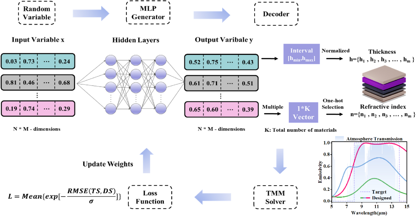
Schematic of the inversed design process for the subwavelength metacoatings. A multilayer perceptron (MLP) generator maps a random variable distribution to a distribution of device with varying thickness and materials by a decoder using predefined rules, evaluated using a transfer matrix method (TMM) solver, and the resulting loss function is used to update the network weights through backpropagation, enabling the optimization to the setting targets.
Figure 2(a) illustrates the MMC structure generated by DNN optimizer, comprising six layers with the following composition and thicknesses: Ge (240 nm), YbF3 (517 nm), Bi (187 nm), Ti (28 nm), Ge (124 nm), and Cr (100 nm). The theoretical emission spectrum of optimized MMC device depicted by the solid line in Figure 2(b), demonstrates good agreement with the ideal LWIR camouflage spectra, represented by the dotted line. Specifically, the optimized MMC structure exhibits an average emissivity of 0.96 within the LWIR atmospheric transmission window (ATW) and a low average emissivity of 0.25 in other mid-infrared (MIR) bands, thereby achieving the desired spectral characteristics for effective LWIR camouflage.
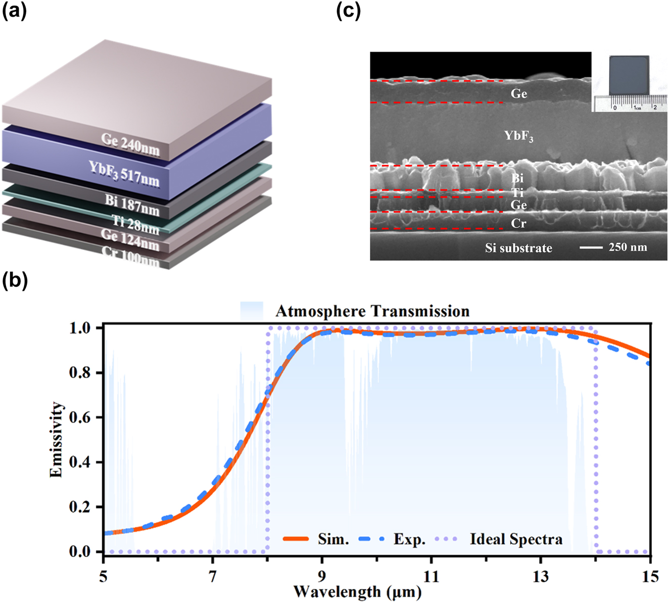
Multilayered metacoating (MMC) for infrared camouflage concept and fabrication. (a) Illustration schematically depicting the proposed MMC. (b) Emissivity spectra for the MMC, where the simulation results (orange line) and experimental measurements (blue dash line) are presented. The comparison includes the ideal high thermal radiation background spectra (purple dot line) and the atmospheric transmission spectra (blue-shaded area). (c) The cross-section SEM and top-view optical images of the experimental sample.
To provide theoretical insights, numerical simulations and calculations were conducted. As shown in Figure 3(a), the normalized power loss spectra for the total and individual components of the MMC device were examined. Most of the power dissipation occurs in the high-loss layers, such as Bi, Ti, and Cr. On average, over 55 % of the incident wave energy is absorbed by the Bi layer in the LWIR band, while the Ti and Cr layers dissipate approximately 30 % and 10 %, respectively. This remarkable energy dissipation is strongly correlated to the unique optical properties of Bi (exhibiting a high refractive index and large absorption coefficient in the MIR band) [46], [47], and Ti (possessing strong optical absorption despite its extremely small thickness). The measured optical properties of these materials are shown in Section S2 of the supplementary Material. We further investigated the mechanism underlying the MMC device’s highly efficient absorption over the LWIR ATW. Since the bottom Cr film is sufficiently thick to prevent light transmission, maximizing absorption involves minimizing reflection, which can be analyzed through optical impedance (Z). The optical impedance Z, used here to analyze the emission properties, is given by the normalized expression Z = Z eff/Z 0, with Z 0 = 377Ω denoting the free-space impedance and Z eff representing the absolute impedance of the MMC structure. As illustrated in Figure 3(b–d), the optical impedance locus of the proposed MMC was examined at different resonance wavelengths (see Section S3 of the supplementary material for detailed numerical computations) as the thickness of various layers increased. The point (1,0) on the chart represents perfect absorption, indicating ideal impedance matching to free space. The purple short-dotted circles represent the impedance trajectory where absorption equals 95 %. It was observed that the optical impedance locus of the MMC device, though initially far from the perfect absorption point, consistently falls within the 95 % absorption circle as the structural parameters approach the design configuration at the typical wavelengths (9.5, 11.0, 13.0 μm), indicating that the condition of impedance matching is reasonably well satisfied in the total working band.
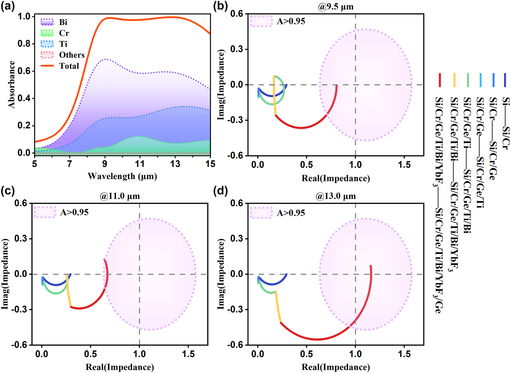
Power dissipation mechanism and optical impedance of the MMC device. (a) The normalized power loss spectra for the total and individual components of the proposed structure. (b–d) The trends of the optical impedance (Z) of the MMC layered by layered at the three resonant wavelengths of 9.5, 11.0, and 13.0 μm. The purple short-dotted circles represent the impedances as A > 0.95.
To gain a more comprehensive understanding of the mechanism behind broadband emission, the finite-difference time-domain (FDTD) method was used to analyze the distributions of electromagnetic fields and energy dissipation within the proposed structure, excited by a plane wave incident perpendicular to the MMC emitter. The simulated results revealed that the magnetic field is concentrated in three distinct regions: the YbF3 layer, the interface between the Bi and Ti layers, and the interface of the underlying Ge and Cr layers, while the electric field is predominantly concentrated at the interface between the YbF3 and Bi layers. Specifically, Figure 4(a) displays the field distributions at the wavelength of 9.5 μm, where the magnetic field is localized in those aforementioned areas and the electric field is slightly concentrated at the interface between YbF3 and Bi. At 11.0 μm, as shown in Figure 4(b), the localization of the magnetic field in the YbF3 layer has diminished, while the other regions maintain a strongly localized magnetic field. Concurrently, the electric field in the interface of YbF3 and Bi increases. Moving to the longer wavelength of 13.0 μm, Figure 4(c) indicates that the localization of the magnetic field in the YbF3 layer further weakens, and the electric field displays a downward trend inside the structure without obvious localization. These field localizations correspond to the energy dissipation within the high-lossy materials in their vicinity. Figure 4(a–c) reveal that the energy loss within the Bi layer decreases with increasing wavelength, which is attributed to the continuous decrease in the localization of the magnetic field within the nearby YbF3 layer. Since the magnetic field maintains a higher level of localization in the other regions, the Ti layer sustains a high absorption, while the absorption of the Cr layer remains relatively stable, consistent with the observations in Figure 3(a). The results indicate that the structure consistently exhibits high energy dissipation characteristics through various forms of electromagnetic field localization across the LWIR spectral region, which is critical for achieving broadband emission. These findings confirm that the broadband emission characteristics depend critically on both the engineered field localization within the precisely optimized MMC’s multilayer structure and the selection of high-loss materials (Bi/Ti). The phenomenon is driven by multiple localized dielectric cavities that confine light, where the adjacent Bi/Ti layers efficiently dissipate the confined energy, resulting in high energy dissipation across a wide LWIR bandwidth. A detailed analysis of the impact of the thickness of each layer of the metacoating on its emission properties is provided in Section S4 of the supplementary material.
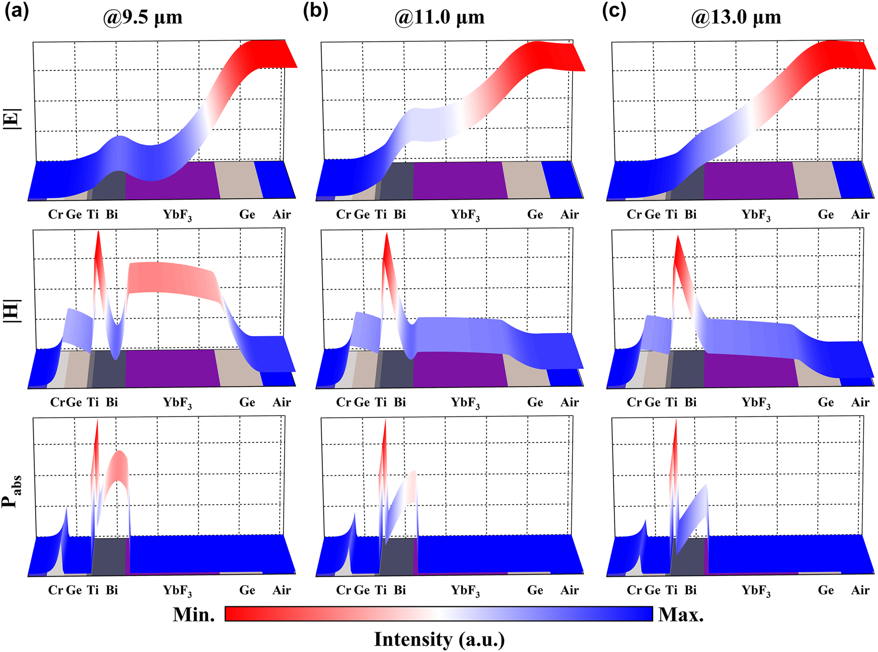
(a–c) Simulated normalized electric field, magnetic field, and time-averaged power dissipation distribution at 9.5 μm, 11.0 μm, and 13.0 μm, respectively.
To experimentally validate the proposed design, the MMC devices were fabricated using electron beam evaporation, as detailed in the Experimental Section. The measured emissivity spectra of the fabricated devices are presented in Figure 2(b) as short-dashed lines, demonstrating excellent agreement with the theoretical results. This correlation between experimental and theoretical results confirms the guidance of the design optimization process. The morphology of the metacoating was characterized using scanning electron microscopy (SEM), and a wafer-scale sample’s optical image is displayed in Figure 2(c). Notably, the prototype device exhibits remarkable deep-subwavelength characteristics, with a total thickness of only 1,220 nm, which is less than one-tenth of the maximum working wavelength.
To evaluate the thermal infrared camouflage performance of the proposed MMC emitter, two distinct experimental setups were employed. In the first experiment, the MMC emitter and a metallic reference sample (a 200 nm Cr film) that has low emissivity across LWIR spectral region were positioned on the author’s palm side by side, as confirmed by the optical image in Figure 5(a). The thermal emission profile was recorded with an LWIR camera (8–14 μm) under ambient temperature conditions, with results depicted in Figure 5(b). The metallic reference sample displayed strong infrared contrast against the palm background due to its distinct thermal radiation properties. In striking contrast, the MMC emitter achieved exceptional infrared camouflage, becoming virtually indistinguishable from the palm background. This remarkable performance stems from the precisely engineered thermal emission characteristics of the MMC emitter, which closely mimics the high emissivity of the human palm.
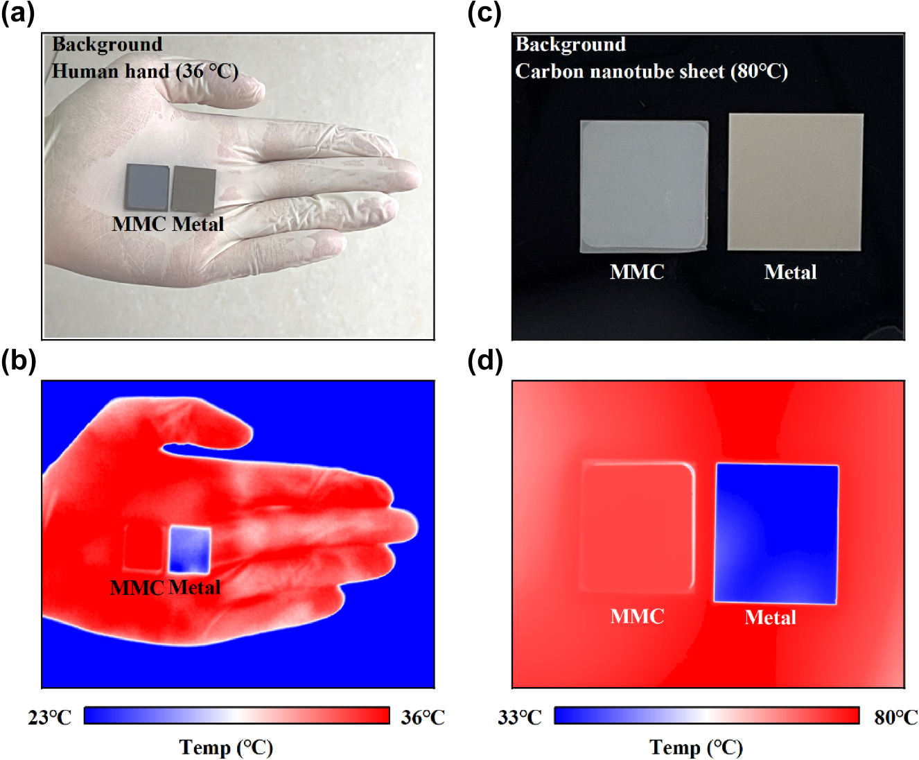
(a) Optical and (b) infrared images of the MC and metal samples placed on the author’s palm. (c) Optical and (d) infrared images of the fabricated samples and reference samples were placed on a carbon nanotube sheet that was mounted on a heating stage and the temperature was set as 80 °C.
The second experiment involved placing the samples on a carbon nanotube sheet mounted on a heated stage maintained at 80 °C. The carbon nanotube substrate is distinguished by its broadband super-black behavior, with detailed emissivity and radiance properties provided in Section S5 of the supplementary material. Figure 5(c) and (d) present the optical and LWIR images of this case, respectively. While the metallic reference sample remained discernible in the infrared image, the MMC emitter demonstrated superior camouflage performance against the high-emissivity carbon nanotube background. The experimental validation involved two distinct high-emission backgrounds to rigorously assess the MMC emitter’s camouflage capabilities. In the first scenario, the MMC sample became virtually indistinguishable from a human palm (ε < 1), a common real-world background with moderate emissivity. This exceptional performance confirms that the MMC’s precisely engineered thermal emission successfully mimics the spectral characteristics of natural skin. In the second scenario, the sample was evaluated against a carbon nanotube (CNT) sheet – a near-blackbody surface with broadband, high emissivity. The MMC emitter again demonstrated superior camouflage, seamlessly blending into the high-emissivity background, whereas the metallic reference remained clearly visible. Both these experiments conclusively validate the MMC emitter’s practical applicability for infrared camouflage.
The angular performance of the proposed MMC emitter was comprehensively characterized through measurements spanning an angular range of 30–80°. Figure 6(a–c) illustrate the experimental emissivity as functions of wavelength and incident angle for s-polarized, p-polarized, and unpolarized light. The results reveal the emitter’s robust angular performance, sustaining an average LWIR emissivity exceeding 0.9 up to a 70° incidence angle across all polarizations. The theoretical spectra, calculated via the transfer matrix method (TMM), are displayed in Figure 6(d–f), exhibiting excellent consistency with the experimental findings. The MMC emitter’s angle-independent emission behavior is attributed to its deep-subwavelength thickness of merely 1.2 μm, a dimension substantially smaller than the wavelengths in the LWIR region. Additionally, its impedance matching property, detailed in Section S6 of the supplementary material, further contributes to this phenomenon. To underscore the practical significance of this angular insensitivity, Figure 6(g) presents infrared images captured in the second experimental scenario (heated carbon nanotube sheet background) at various observation angles. Notably, even at a large oblique angle of 70°, the MMC emitter retains its effective camouflage capability, seamlessly blending into the high-radiation background. This further demonstrates the emitter’s potential for real-world thermal infrared camouflage applications.
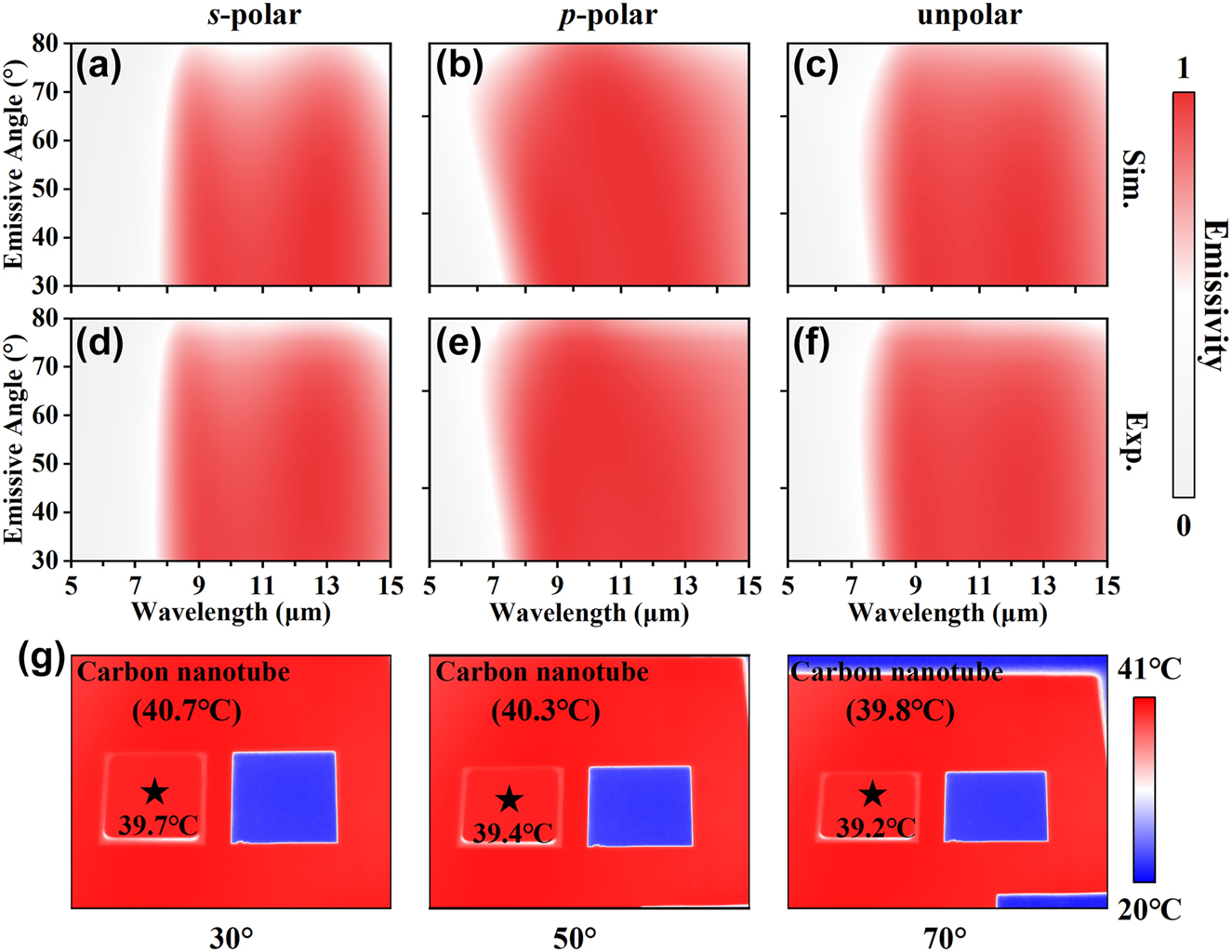
(a–c) Simulated and (d–f) experimental measured spectra as a function of wavelengths and incident angles for s-, p-, and unpolar light, respectively. (g) Infrared images of the MMC and metal samples placed on the carbon nanotube captured at different observation angles (30°, 50°, 70°).
3 Conclusions
In conclusion, this work has proposed and experimentally demonstrated a broadband, lithography-free, ultra-thin, high-performance metacoating emitter for LWIR camouflage applications in high-emission environments. The optimized MMC emitter was developed through an automated framework empowered by a DNN optimizer. The resulting emitter exhibits an exceptional average emissivity exceeding 0.96 across the LWIR ATW, while maintaining a low emissivity below 0.25 in the other MIR spectral region, as validated by both experimental and theoretical analyses. The outstanding thermal emission characteristics of the MMC emitter can be primarily attributed to its broadband impedance matching design, which facilitates efficient energy dissipation through localized EM field confinement within the multi-layer structure, particularly in the proximity of high-lossy Bi and Ti components. Furthermore, IR imaging experiments were conducted to directly showcase the superior camouflage performance of the proposed emitter against highly radiative backgrounds. Importantly, the deep-subwavelength thickness (1.22 μm) of the MMC structure confers angle-independent emission properties, with the favorable emissive behavior (∼0.9 emissivity) being maintained even at large incidence angles up to 70°. This angular robustness would be an asset in real-world thermal IR camouflage applications, as it enables effective concealment against modern detection methods employing wide-angle and polarization-sensitive measurements. The findings of this work indicate the significant potential of the developed MMC emitter for advanced IR camouflage applications.
4 Materials and methods
4.1 Optical constants measurement
The optical constants of the deposited layers Cr, Ge, Ti, Bi, and YbF3 were measured and fitted in the infrared range using infrared spectroscopic ellipsometry (Sendira Sentech, 1,500–25,000 nm) and the optical constants of Au, Ag, Al, Ti, MgF2, Si, ZnS, SiO2, HfO2 were obtained from literature [50].
4.2 Numerical computations and simulations
The numerical computations were carried out through transfer matrix methods (TMM). Electromagnetic wave numerical simulations were conducted based on finite-difference-time-domain (FDTD) method. In the simulations, a plane source was launched into a two-dimensional FDTD simulation zone. Periodic boundary conditions were imposed on the x axes, and perfect matched layer (PML) were imposed on the y axes.
4.3 Sample fabrication and characterization
The samples and reference sample were fabricated by electron-beam evaporation (Syskey Technology UHEB-LC6-03) based on layer-by-layer deposition process. The Ge, YbF3, Bi, Ti and Cr layers were deposited at room temperature at rates of 0.3 nm/s, 0.6 nm/s, 0.2 nm/s, 0.2 nm/s and 0.1 nm/s, respectively. The deposition rates were monitored by gold coated crystals (Inficon) and the chamber pressure were maintained at ∼10-6 Torr (Pfeiffer) during the deposition process. The cross-section of the sample was characterized by scanning electron microscopy (FEI Sirion 200).
The angle-resolved reflectance spectra over a range of 30–80° were obtained using a Fourier transform infrared spectrometer (Thermo Scientific Nicolet iS50), both covering a spectral range of 8,000–400 cm−1. Additionally, the morphologies of the proposed MMC were characterized using a scanning electron microscope (FEI Sirion 200) with an accelerating voltage of 10 kV. Thermal measurements were conducted using an LWIR camera (Fotric 220) with a default emissivity of 0.95, operating in the 8–14 μm wavelength range.
Funding source: National Natural Science Foundation of China
Award Identifier / Grant number: 11933006
Award Identifier / Grant number: 62075231
Award Identifier / Grant number: U2141240
Funding source: Shanghai Science and Technology Committee
Award Identifier / Grant number: 20JC1414603
Award Identifier / Grant number: 23ZR1473300
Award Identifier / Grant number: 23dz2260100
Funding source: National Key Research and Development Program of China
Award Identifier / Grant number: 2022YFA1404701
Funding source: Shanghai Innovation Project
Award Identifier / Grant number: 2021-cyxt1-kj04
-
Research funding: This work was supported by the National Key R&D Program of China (2022YFA1404700), National Natural Science Foundation of China (U2141240, 62075231), Shanghai Science and Technology Committee (23dz2260100, 23ZR1473300).
-
Author contributions: QQ: conceptualization, methodology, software, investigation, validation, formal analysis, visualization, writing original draft. KL: investigation, validation, visualization, writing review & editing. DZ: investigation, validation, visualization, writing review & editing. YZ: formal analysis, validation. JZ: investigation, validation. ZZ: investigation, validation. YS: resources, supervision, investigation, validation, funding acquisition. LZ: resources, supervision, funding acquisition. ND: resources, supervision, funding acquisition. JC: resources, supervision, funding acquisition. JH: conceptualization, methodology, validation, formal analysis, writing review & editing, resources, supervision, project administration, funding acquisition. All authors have accepted responsibility for the entire content of this manuscript and consented to its submission to the journal, reviewed all the results and approved the final version of the manuscript.
-
Conflict of interest: Authors state no conflicts of interest.
-
Data availability: All data are available in the main text or the Supplementary Materials. Requests should be directed to the corresponding authors.
References
[1] D. G. Baranov, Y. Xiao, I. A. Nechepurenko, A. Krasnok, A. Alù, and M. A. Kats, “Nanophotonic engineering of far-field thermal emitters,” Nat. Mater., vol. 18, no. 9, pp. 920–930, 2019. https://doi.org/10.1038/s41563-019-0363-y.Search in Google Scholar PubMed
[2] X. Pan et al.., “Spatial and frequency selective plasmonic metasurface for long wavelength Infrared spectral region,” Adv. Opt. Mater., vol. 6, no. 20, p. 1800337, 2018. https://doi.org/10.1002/adom.201800337.Search in Google Scholar
[3] B. Qin, Y. Zhu, Y. Zhou, M. Qiu, and Q. Li, “Whole-infrared-band camouflage with dual-band radiative heat dissipation,” Light Sci. Appl., vol. 12, p. 246, 2023, https://doi.org/10.1038/s41377-023-01287-z.Search in Google Scholar PubMed PubMed Central
[4] J. Zhou et al.., “Angle-selective thermal emitter for directional radiative cooling and heating,” Joule, vol. 7, no. 12, pp. 2830–2844, 2023. https://doi.org/10.1016/j.joule.2023.10.013.Search in Google Scholar
[5] A. P. Raman, M. A. Anoma, L. Zhu, E. Rephaeli, and S. Fan, “Passive radiative cooling below ambient air temperature under direct sunlight,” Nature, vol. 515, no. 7528, pp. 540–544, 2014. https://doi.org/10.1038/nature13883.Search in Google Scholar PubMed
[6] M.-T. Tsai et al.., “Scalable, flame-resistant, superhydrophobic ceramic metafibers for sustainable all-day radiative cooling,” Nano Today, vol. 48, p. 101745, 2023, https://doi.org/10.1016/j.nantod.2022.101745.Search in Google Scholar
[7] M. Dirnwoeber, R. Machan, and J. Herler, “Coral reef surveillance: Infrared-sensitive video surveillance technology as a new tool for diurnal and nocturnal long-term field observations,” Remote Sens-Basel, vol. 4, no. 11, pp. 3346–3362, 2012. https://doi.org/10.3390/rs4113346.Search in Google Scholar PubMed PubMed Central
[8] P. Martyniuk, J. Antoszewski, M. Martyniuk, L. Faraone, and A. Rogalski, “New concepts in infrared photodetector designs,” Appl. Phys. Rev., vol. 1, no. 4, p. 041102, 2014. https://doi.org/10.1063/1.4896193.Search in Google Scholar
[9] Z. Zhou et al.., “Surface plasmon enhanced InAs-based mid-wavelength infrared photodetector,” Appl. Phys. Lett., vol. 122, no. 9, p. 091105, 2023. https://doi.org/10.1063/5.0140370.Search in Google Scholar
[10] Z. Zhou et al.., “Narrowband HgCdTe infrared photodetector with integrated plasmonic structure,” Opt. Lett., vol. 48, no. 7, p. 1882, 2023. https://doi.org/10.1364/ol.486788.Search in Google Scholar
[11] J. E. Vázquez-Lozano and I. Liberal, “Review on the scientific and technological breakthroughs in thermal emission engineering,” ACS Appl. Opt. Mater., vol. 2, no. 6, pp. 896–1244, 2024. https://doi.org/10.1021/acsaom.4c00030.Search in Google Scholar PubMed PubMed Central
[12] B. Wang, X. Qin, G. Duan, G. Yang, W. Huang, and Z. Huang, “Dielectric‐based metamaterials for near‐perfect light absorption,” Adv. Funct. Mater., vol. 34, no. 37, p. 2402068, 2024. https://doi.org/10.1002/adfm.202402068.Search in Google Scholar
[13] J. Zhang, R. Wei, M. ElKabbash, E. M. Campbell, and C. Guo, “Thin-film perfect infrared absorbers over single- and dual-band atmospheric windows,” Opt. Lett., vol. 45, no. 10, p. 2800, 2020. https://doi.org/10.1364/ol.392651.Search in Google Scholar PubMed
[14] Q. Chu, F. Zhong, X. Shang, Y. Zhang, S. Zhu, and H. Liu, “Controlling thermal emission with metasurfaces and its applications,” Nanophotonics, vol. 13, no. 8, pp. 1279–1301, 2024. https://doi.org/10.1515/nanoph-2023-0754.Search in Google Scholar PubMed PubMed Central
[15] R. Hu et al.., “Thermal camouflaging metamaterials,” Mater. Today, vol. 45, pp. 120–141, 2021, https://doi.org/10.1016/j.mattod.2020.11.013.Search in Google Scholar
[16] S. Dang and H. Ye, “A visible-infrared-compatible camouflage photonic crystal with heat dissipation by radiation in 5–8 μm,” Cell Rep. Phys. Sci., vol. 2, no. 11, p. 100617, 2021. https://doi.org/10.1016/j.xcrp.2021.100617.Search in Google Scholar
[17] L. Huang et al.., “Multiband camouflage design with thermal management,” Photon. Res., vol. 11, no. 5, p. 839, 2023. https://doi.org/10.1364/prj.484448.Search in Google Scholar
[18] I. Celanovic, N. Jovanovic, and J. Kassakian, “Two-dimensional tungsten photonic crystals as selective thermal emitters,” Appl. Phys. Lett., vol. 92, no. 19, p. 193101, 2008. https://doi.org/10.1063/1.2927484.Search in Google Scholar
[19] J. Zhang et al.., “Long-wavelength infrared selective emitter for thermal infrared camouflage under a hot environment,” Opt. Express., vol. 30, no. 13, p. 24132, 2022. https://doi.org/10.1364/oe.462166.Search in Google Scholar PubMed
[20] J. Kim, C. Park, and J. W. Hahn, “Metal–semiconductor–metal metasurface for multiband infrared stealth technology using camouflage color pattern in visible range,” Adv. Opt. Mater., vol. 10, no. 6, p. 2101930, 2022. https://doi.org/10.1002/adom.202101930.Search in Google Scholar
[21] Y. Liu, Z. Feng, C. Xu, A. Chatterjee, and A. A. Gorodetsky, “Reconfigurable Micro- and nano-structured camouflage surfaces inspired by cephalopods,” ACS Nano, vol. 15, no. 11, pp. 17299–17309, 2021. https://doi.org/10.1021/acsnano.0c09990.Search in Google Scholar PubMed
[22] D. Zhou et al.., “Semimetal–dielectric–metal metasurface for infrared camouflage with high-performance energy dissipation in non-atmospheric transparency window,” Nanophotonics, vol. 14, no. 8, pp. 1101–1111, 2025. https://doi.org/10.1515/nanoph-2024-0538.Search in Google Scholar PubMed PubMed Central
[23] X. Ruan et al.., “Ultrathin, broadband, omnidirectional, and polarization-independent infrared absorber using all-dielectric refractory materials,” Nanophotonics, vol. 10, no. 6, pp. 1683–1690, 2021. https://doi.org/10.1515/nanoph-2020-0627.Search in Google Scholar
[24] M. J. Moghimi, G. Lin, and H. Jiang, “Broadband and ultrathin infrared stealth sheets,” Adv. Eng. Mater., vol. 20, no. 11, p. 1800038, 2018. https://doi.org/10.1002/adem.201800038.Search in Google Scholar
[25] W. Xi et al.., “Ultrahigh-efficient material informatics inverse design of thermal metamaterials for visible-infrared-compatible camouflage,” Nat. Commun., vol. 14, p. 4694, 2023, https://doi.org/10.1038/s41467-023-40350-6.Search in Google Scholar PubMed PubMed Central
[26] Y. Li et al.., “Scalable‐manufactured plasmonic metamaterial with omnidirectional absorption bandwidth across visible to far‐infrared,” Adv. Funct. Mater., vol. 32, no. 46, p. 2207239, 2022. https://doi.org/10.1002/adfm.202207239.Search in Google Scholar
[27] H. Zhang et al.., “Super broadband mid-infrared absorbers with ultrathin folded highly-lossy films,” J. Colloid Interface Sci., vol. 629, pp. 254–262, 2023, https://doi.org/10.1016/j.jcis.2022.09.046.Search in Google Scholar PubMed
[28] C. Yang, Y. Liu, S. Xie, and Z. Guo, “PDMS-based photothermal super-ice-repellent films with bendable stretchability and efficient anti-icing/de-icing properties,” Nano Today, vol. 62, p. 102704, 2025, https://doi.org/10.1016/j.nantod.2025.102704.Search in Google Scholar
[29] B. Leng, Y. Zhang, D. P. Tsai, and S. Xiao, “Meta-device: Advanced manufacturing,” Light Adv. Manu., vol. 5, no. 1, p. 5, 2024. https://doi.org/10.37188/lam.2024.005.Search in Google Scholar
[30] J. Toudert, R. Serna, M. G. Pardo, N. Ramos, R. J. Peláez, and B. Maté, “Mid-to-far infrared tunable perfect absorption by a sub - λ/100 nanofilm in a fractal phasor resonant cavity,” Opt. Express., vol. 26, no. 26, p. 34043, 2018. https://doi.org/10.1364/oe.26.034043.Search in Google Scholar PubMed
[31] W. Wang et al.., “Broadband thin-film and metamaterial absorbers using refractory vanadium nitride and their thermal stability,” Opt. Express., vol. 29, no. 21, p. 33456, 2021. https://doi.org/10.1364/oe.439546.Search in Google Scholar PubMed
[32] Z. Deng, Y. Su, W. Qin, T. Wang, X. Wang, and R. Gong, “Nanostructured Ge/ZnS films for multispectral camouflage with low visibility and low thermal emission,” ACS Appl. Nano Mater., vol. 5, no. 4, pp. 5119–5127, 2022. https://doi.org/10.1021/acsanm.2c00088.Search in Google Scholar
[33] M. He et al.., “Deterministic inverse design of Tamm plasmon thermal emitters with multi-resonant control,” Nat. Mater., vol. 20, no. 10, pp. 1663–1669, 2021. https://doi.org/10.1038/s41563-021-01094-0.Search in Google Scholar PubMed
[34] C. Wang et al.., “Multifunctional wearable thermal management textile fabricated by one-step sputtering,” Nano Today, vol. 45, p. 101526, 2022, https://doi.org/10.1016/j.nantod.2022.101526.Search in Google Scholar
[35] X. Jiang et al.., “Implementing of infrared camouflage with thermal management based on inverse design and hierarchical metamaterial,” Nanophotonics, vol. 12, no. 10, pp. 1891–1902, 2023. https://doi.org/10.1515/nanoph-2023-0067.Search in Google Scholar PubMed PubMed Central
[36] M. Li, D. Liu, H. Cheng, L. Peng, and M. Zu, “Manipulating metals for adaptive thermal camouflage,” Sci. Adv., vol. 6, no. 22, p. eaba3934, 2020. https://doi.org/10.1126/sciadv.aba3494.Search in Google Scholar PubMed PubMed Central
[37] D. Zhou et al.., “Subwavelength broadband light-harvesting metacoating for infrared camouflage and anti-counterfeiting empowered by inverse design,” Mater. Today Phys., vol. 50, p. 101614, 2025, https://doi.org/10.1016/j.mtphys.2024.101614.Search in Google Scholar
[38] C. Tan et al.., “Deep-subwavelength multilayered meta-coatings for visible-infrared compatible camouflage,” Nanophotonics, vol. 13, no. 13, pp. 2391–2400, 2024. https://doi.org/10.1515/nanoph-2024-0029.Search in Google Scholar PubMed PubMed Central
[39] Z. Ren et al.., “Infrared camouflage based on the crystalline and amorphous GST multilayer films,” Appl. Phys. Lett., vol. 121, no. 25, p. 253504, 2022. https://doi.org/10.1063/5.0134673.Search in Google Scholar
[40] Y. Xiong, Y. Zhou, J. Tian, W. Wang, W. Zhang, and D. Zhang, “Scalable, color‐matched, flexible plasmonic film for visible–infrared compatible camouflage,” Adv. Sci., vol. 10, no. 35, p. 2303452, 2023. https://doi.org/10.1002/advs.202303452.Search in Google Scholar PubMed PubMed Central
[41] N. Wang, W. Yan, Y. Qu, S. Ma, S. Z. Li, and M. Qiu, “Intelligent designs in nanophotonics: From optimization towards inverse creation,” PhotoniX, vol. 2, p. 22, 2021, https://doi.org/10.1186/s43074-021-00044-y.Search in Google Scholar
[42] S. Molesky, Z. Lin, A. Y. Piggott, W. Jin, J. Vucković, and A. W. Rodriguez, “Inverse design in nanophotonics,” Nat. Photon., vol. 12, no. 10, pp. 659–670, 2018. https://doi.org/10.1038/s41566-018-0246-9.Search in Google Scholar
[43] A. Sakurai et al.., “Ultranarrow-band wavelength-selective thermal emission with aperiodic multilayered metamaterials designed by bayesian optimization,” ACS Cent. Sci., vol. 5, no. 2, pp. 319–326, 2019. https://doi.org/10.1021/acscentsci.8b00802.Search in Google Scholar PubMed PubMed Central
[44] S. Yu et al.., “General deep learning framework for emissivity engineering,” Light Sci. Appl., vol. 12, p. 291, 2023, https://doi.org/10.1038/s41377-023-01341-w.Search in Google Scholar PubMed PubMed Central
[45] P. Dai et al.., “Accurate inverse design of Fabry–Perot-cavity-based color filters far beyond sRGB via a bidirectional artificial neural network,” Photon. Res., vol. 9, no. 5, p. B236, 2021. https://doi.org/10.1364/prj.415141.Search in Google Scholar
[46] Q. Guan, A. Raza, S. S. Mao, L. F. Vega, and T. Zhang, “Machine learning-enabled inverse design of radiative cooling film with On-Demand transmissive color,” ACS Photonics, vol. 10, no. 3, pp. 715–726, 2023. https://doi.org/10.1021/acsphotonics.2c01857.Search in Google Scholar
[47] J. Jiang and J. A. Fan, “Simulator-based training of generative neural networks for the inverse design of metasurfaces,” Nanophotonics, vol. 9, no. 5, pp. 1059–1069, 2019. https://doi.org/10.1515/nanoph-2019-0330.Search in Google Scholar
[48] J. Jiang and J. A. Fan, “Multiobjective and categorical global optimization of photonic structures based on ResNet generative neural networks,” Nanophotonics, vol. 10, no. 1, pp. 361–369, 2020. https://doi.org/10.1515/nanoph-2020-0407.Search in Google Scholar
[49] D. E. Rumelhart, G. E. Hinton, and R. J. Williams, “Learning representations by back-propagating errors,” Nature, vol. 323, no. 6088, pp. 533–536, 1986. https://doi.org/10.1038/323533a0.Search in Google Scholar
[50] E. D. Palik, Handbook of Optical Constants of Solids, San Diego, Academic Press, 1998.Search in Google Scholar
Supplementary Material
This article contains supplementary material (https://doi.org/10.1515/nanoph-2025-0409).
© 2025 the author(s), published by De Gruyter, Berlin/Boston
This work is licensed under the Creative Commons Attribution 4.0 International License.
Articles in the same Issue
- Frontmatter
- Reviews
- Light-driven micro/nanobots
- Tunable BIC metamaterials with Dirac semimetals
- Large-scale silicon photonics switches for AI/ML interconnections based on a 300-mm CMOS pilot line
- Perspective
- Density-functional tight binding meets Maxwell: unraveling the mysteries of (strong) light–matter coupling efficiently
- Letters
- Broadband on-chip spectral sensing via directly integrated narrowband plasmonic filters for computational multispectral imaging
- Sub-100 nm manipulation of blue light over a large field of view using Si nanolens array
- Tunable bound states in the continuum through hybridization of 1D and 2D metasurfaces
- Integrated array of coupled exciton–polariton condensates
- Disentangling the absorption lineshape of methylene blue for nanocavity strong coupling
- Research Articles
- Demonstration of multiple-wavelength-band photonic integrated circuits using a silicon and silicon nitride 2.5D integration method
- Inverse-designed gyrotropic scatterers for non-reciprocal analog computing
- Highly sensitive broadband photodetector based on PtSe2 photothermal effect and fiber harmonic Vernier effect
- Online training and pruning of multi-wavelength photonic neural networks
- Robust transport of high-speed data in a topological valley Hall insulator
- Engineering super- and sub-radiant hybrid plasmons in a tunable graphene frame-heptamer metasurface
- Near-unity fueling light into a single plasmonic nanocavity
- Polarization-dependent gain characterization in x-cut LNOI erbium-doped waveguide amplifiers
- Intramodal stimulated Brillouin scattering in suspended AlN waveguides
- Single-shot Stokes polarimetry of plasmon-coupled single-molecule fluorescence
- Metastructure-enabled scalable multiple mode-order converters: conceptual design and demonstration in direct-access add/drop multiplexing systems
- High-sensitivity U-shaped biosensor for rabbit IgG detection based on PDA/AuNPs/PDA sandwich structure
- Deep-learning-based polarization-dependent switching metasurface in dual-band for optical communication
- A nonlocal metasurface for optical edge detection in the far-field
- Coexistence of weak and strong coupling in a photonic molecule through dissipative coupling to a quantum dot
- Mitigate the variation of energy band gap with electric field induced by quantum confinement Stark effect via a gradient quantum system for frequency-stable laser diodes
- Orthogonal canalized polaritons via coupling graphene plasmon and phonon polaritons of hBN metasurface
- Dual-polarization electromagnetic window simultaneously with extreme in-band angle-stability and out-of-band RCS reduction empowered by flip-coding metasurface
- Record-level, exceptionally broadband borophene-based absorber with near-perfect absorption: design and comparison with a graphene-based counterpart
- Generalized non-Hermitian Hamiltonian for guided resonances in photonic crystal slabs
- A 10× continuously zoomable metalens system with super-wide field of view and near-diffraction–limited resolution
- Continuously tunable broadband adiabatic coupler for programmable photonic processors
- Diffraction order-engineered polarization-dependent silicon nano-antennas metagrating for compact subtissue Mueller microscopy
- Lithography-free subwavelength metacoatings for high thermal radiation background camouflage empowered by deep neural network
- Multicolor nanoring arrays with uniform and decoupled scattering for augmented reality displays
- Permittivity-asymmetric qBIC metasurfaces for refractive index sensing
- Theory of dynamical superradiance in organic materials
- Second-harmonic generation in NbOI2-integrated silicon nitride microdisk resonators
- A comprehensive study of plasmonic mode hybridization in gold nanoparticle-over-mirror (NPoM) arrays
- Foundry-enabled wafer-scale characterization and modeling of silicon photonic DWDM links
- Rough Fabry–Perot cavity: a vastly multi-scale numerical problem
- Classification of quantum-spin-hall topological phase in 2D photonic continuous media using electromagnetic parameters
- Light-guided spectral sculpting in chiral azobenzene-doped cholesteric liquid crystals for reconfigurable narrowband unpolarized light sources
- Modelling Purcell enhancement of metasurfaces supporting quasi-bound states in the continuum
- Ultranarrow polaritonic cavities formed by one-dimensional junctions of two-dimensional in-plane heterostructures
- Bridging the scalability gap in van der Waals light guiding with high refractive index MoTe2
- Ultrafast optical modulation of vibrational strong coupling in ReCl(CO)3(2,2-bipyridine)
- Chirality-driven all-optical image differentiation
- Wafer-scale CMOS foundry silicon-on-insulator devices for integrated temporal pulse compression
- Monolithic temperature-insensitive high-Q Ta2O5 microdisk resonator
- Nanogap-enhanced terahertz suppression of superconductivity
- Large-gap cascaded Moiré metasurfaces enabling switchable bright-field and phase-contrast imaging compatible with coherent and incoherent light
- Synergistic enhancement of magneto-optical response in cobalt-based metasurfaces via plasmonic, lattice, and cavity modes
- Scalable unitary computing using time-parallelized photonic lattices
- Diffusion model-based inverse design of photonic crystals for customized refraction
- Wafer-scale integration of photonic integrated circuits and atomic vapor cells
- Optical see-through augmented reality via inverse-designed waveguide couplers
- One-dimensional dielectric grating structure for plasmonic coupling and routing
- MCP-enabled LLM for meta-optics inverse design: leveraging differentiable solver without LLM expertise
- Broadband variable beamsplitter made of a subwavelength-thick metamaterial
- Scaling-dependent tunability of spin-driven photocurrents in magnetic metamaterials
- AI-based analysis algorithm incorporating nanoscale structural variations and measurement-angle misalignment in spectroscopic ellipsometry