Wafer-scale CMOS foundry silicon-on-insulator devices for integrated temporal pulse compression
-
Ju Won Choi
 ,
Kenny Y.K. Ong
,
Kenny Y.K. Ong


Abstract
Optical pulses are essential as information carriers, for driving nonlinear light sources, imaging, the study of attosecond science and 3D printing. In many applications, short pulses are needed. For example, the resolution of imaging methods which utilize short pulses is limited by the temporal width of the pulses, as is the capacity of time division multiplexed data. The temporal compression of optical pulses is an important approach to achieving ultrashort pulses. With the widespread proliferation of silicon photonics and their use in a multitude of applications, an integrated, CMOS-compatible approach for pulse compression would allow its seamless integration with other photonic integrated circuits. In this work, we experimentally demonstrate silicon-based pulse compression fabricated in a CMOS foundry. The first technique utilizes two stages, one for generating self-phase modulation through the Kerr nonlinearity in silicon, and the second for temporal synchronization of the new wavelengths. The second technique leverages Bragg soliton-effect temporal compression. We experimentally demonstrate temporal compression of up to 3.6× and good agreement with numerical calculations. This work represents efficient silicon-on-insulator devices for temporal compression realized using a wafer-scale CMOS foundry process and may therefore be mass manufactured and integrated seamlessly with other photonic and electronic circuits.
1 Introduction
Temporal compression of optical pulses may leverage the Kerr effect, facilitating access to ultrashort pulses required for a variety of applications including optical imaging and high-speed communications based on optical time division multiplexing (OTDM) [1], [2], [3], [4], [5], [6]. OTDM may further be combined with wavelength multiplexing to augment the aggregate data rate [6], while the temporal compression of optical pulses allows a larger number of pulse trains to be interleaved to achieve a higher overall OTDM rate [7]. Earliest demonstrations of temporal compression utilized bulk optics. In 1969, Treacy reported compression using a diffraction grating pair [8]. Temporal compression involving the Kerr effect was reported by Fischer et al. that same year, forming the foundations for a compression method which is widely used today [9]. In that work, temporal compression utilized nonlinear phase acquisition in an optical Kerr liquid followed by differential optical delays. With advancements in the manufacture of low-loss, high-quality single mode fiber, methods for temporal compression which were once limited to theory could be experimentally demonstrated. Theoretical predictions of fiber-based self-phase modulation combined with a grating pair could be used to temporally compress pulses [10]. In this method of optical pulse compression, the optical pulse undergoes a frequency chirp, prior to rephasing with a dispersive element. This approach decouples nonlinearity and dispersion. In integrated photonics, a waveguide is analogous to bulk crystal used for nonlinear phase acquisition whereas a chirped on-chip grating is used in place of a bulk grating.
In parallel, seminal work from Molleneur set the stage for decades of advancements in optical soliton science, providing new approaches for short pulse generation [11]. Today, the field of solitons is flourishing not just within the optical fiber community but also in integrated photonics. Short pulses may be generated through soliton effects via the initial temporal narrowing experienced by a high order soliton. Contrary to compression using self-phase modulation prior to propagation through a dispersive element, in soliton-effect compression, the nonlinearity and dispersion are distributed over the fiber or waveguide. Bragg-soliton effect compression facilitates strong compression dynamics through the strong grating induced dispersion on the stopband edge [12], [13]. In particular, Bragg soliton phenomena in chip-scale platforms have undergone tremendous advancements in the last few years due to improvements in nanofabrication and the availability of high nonlinear figure of merit platforms [14], [15], [16], [17]. Compared to optical fiber, chip-scale devices may have nonlinear parameters six orders of magnitude larger, enabling significantly lower power operation and smaller form factors to be used [14], [18].
Significant progress has been made in both types of compression in chip-scale devices [19], [20], [21], [22], [23], [24]. In many of these demonstrations, devices with sub-100 nm critical dimensions were required. To achieve the requisite fabrication resolution, electron-beam (e-beam) lithography is typically used. While e-beam allows very high-resolution patterning to be performed, it requires line by line writing which limits the throughput. Conversely, the use of processing techniques which adopt optical lithography (e.g. UV lithography) such as that used in CMOS foundries allows very high throughput manufacture of photonic devices. The research question which needs to be answered is whether designs which work within the limited resolutions available in wafer-scale processes may be successfully established and reduced to practice.
In this paper, we explore nonlinear temporal pulse compression fabricated using an 8-inch wafer-scale CMOS foundry process. We present the design and experimental characterization of two types of nonlinear phenomena for temporal compression in integrated devices, achieving a compression factor of up to 3.6×. We further explore how foundry limitations may be overcome to achieve the required device performance and device limitations arising from the material platform. These results showcase the widescale manufacturability of such devices which thus far have been mainly limited to realization using e-beam lithography and may accelerate their implementation in more complex photonic integrated circuits for applications in high-speed communications and optical sources.
2 Device design
Figure 1 shows the schematic of the device studied in this paper. The device is implemented on the silicon-on-insulator platform with a height, H = 220 nm. All devices have SiO2 under- and over-cladding. Though this is a prolific material in CMOS-wafer scale fabrication of photonics devices, silicon has some drawbacks in nonlinear efficiency due to its small bandgap of 1.1 eV. This results in two-photon absorption (TPA) and free-carrier absorption (FCA) at wavelengths shorter than 2.2 μm including the important telecommunications wavelengths [25], [26]. We analyze the impact of these effects through numerical simulations later. The device shown in Figure 1(a) consists of two sinusoidally modulated gratings which are coupled. The coupled grating has widths, W
1 = 400 nm and W
2 = 500 nm and a length of 4 mm. The maximum modulation amplitude for W
1 and W
2 is 40 nm and 50 nm respectively. The gap between the modulation peaks is 150 nm which is selected such that it may be well resolved by the 8-inch CMOS foundry process used to fabricate the devices. The coupled grating’s modulation amplitude varies from its maximum value at the center of the grating to 0 at the ends in a raised cosine profile to achieve apodization. The average grating pitch, Λ0 is selected to have a stopband within the C-band and varies linearly along the length of the coupled grating according to the expression,
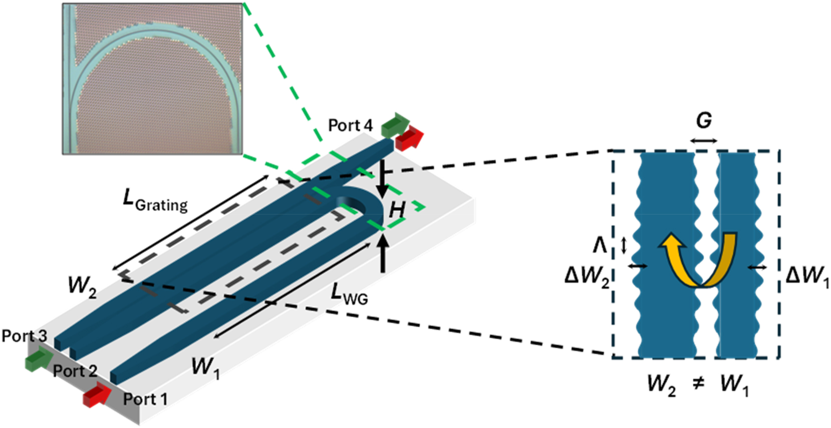
Schematic of the device used for temporal compression. An optical micrograph of the device is shown. Configuration 1 refers to an input at Port 3 and output at Port 4. Configuration 2 refers to an input at Port 1 and output at Port 4.
We describe the two configurations for using the device for temporal compression. Configuration 1 involves launching input pulses at Port 3 and pulses undergo Bragg-soliton effect compression prior to exiting at Port 4. In this configuration, the single grating with width, W
2 generates a stopband within the C-band. The stopband is centered at wavelength,
λ
B
,1, is governed by the equation,
λ
B
,1 = 2 ×
n
eff,2 × Λ, where n
eff2 is the effective index of the grating with width W
2. The blue-side of the grating stopband is characterized as having a rapidly increasing group index as wavelength is increased. Figure 2(a) shows the measured transmission and group index spectrum for the grating with ΔΛ = 0. The transmission spectrum is measured using a broadband light source adjusted for transverse electric polarization and an optical spectrum analyzer, whereas the group index spectrum is measured using a dispersion analyzer. It may be observed that as the wavelength increases from 1556 nm to 1561 nm, the group index undergoes a large increase from 4.2 to 5.4, further indicating a large anomalous dispersion. This large dispersion originates from the interaction between the forward and backward propagating grating modes that are a result of the grating periodicity [27]. In addition, the elevated group index results in an augmented effective nonlinear parameter,

Optical properties of the device when using configuration 1. (a) Measured transmission spectrum and group delay profile for the silicon grating used for temporal compression. The inset shows the group index as a function of wavelength. (b) Measured transmission spectrum of silicon gratings with for ΔΛ from 0 nm to 10 nm. It may be observed that the bandwidth of the stopband increases with ΔΛ.
The second configuration for temporal compression (configuration 2), involves launching input pulses into Port 1 and an output at Port 4. In this configuration, the wavelength of the input pulses needs to be located within the grating stopband. The optical pulses will first undergo self-phase modulation in the 4 mm long silicon waveguide with width W
1. The spectrally broadened pulses will next enter the coupled grating, where cross coupling between gratings with width W
1 and W
2 will generate a stopband centered at wavelength,
We design and fabricate several devices with different values of ΔΛ. All gratings have a length of 4 mm. The transmission spectrum of the gratings when using configuration 1 (input at Port 3 and output at Port 4) is first measured using an amplified spontaneous emission source and optical spectrum analyzer. Light from the source is first aligned for transverse-electric (TE) polarization. Figure 2(b) shows the measured transmission spectra of the gratings where minimal ripple exists in the transmission spectrum. It may also be observed that the bandwidth of grating stopband increases with ΔΛ. The transmission and group delay spectra of the grating with ΔΛ = 0 nm used for the temporal compression measurements in configuration 1 are shown in Figure 2(a). The group delay spectrum is measured using a dispersion analyzer.
Next, the measured transmission spectra for configuration 2 for the devices with different values of ΔΛ are shown in Figure 3(a). It may be observed that the bandwidth of the stopband increases with ΔΛ. The measured dispersion within the stopband as a function of ΔΛ is further shown in Figure 3(b). The achievable dispersion within the range of devices 5.7 × 10⁵ ps/nm/km to 1.1 × 10⁷ ps/nm/km. Figure 3(c) shows the measured transmission and group delay spectrum for ΔΛ = 10 nm, corresponding to a dispersion of 5.7 × 10⁵ ps/nm/km, which will be used for demonstrating pulse compression. It may be observed that the group delay within the stopband is linear, with the delay increasing with wavelength, generating anomalous dispersion.

Optical properties of the device when using configuration 2. (a) The measured transmission spectrum and (b) dispersion for Configuration 2 as a function of chirp. (c) The measured transmission and group delay spectrum within the grating stopband for ΔΛ = 10 nm.
3 Temporal compression characterization
We first study configuration 1 for temporal compression of pulses using the grating shown in Figure 2(a). In this configuration, Bragg soliton-effect compression is leveraged. The wavelength of the optical pulses is located on the blue side of the stopband edge, varied between 1548 nm–1558 nm. We first characterize the output of 1.4 ps pulses at a fixed input peak power of 12.5 W as a function of the pulse wavelength. The measured output pulse width is shown in Figure 4(a) while Figure 4(b) shows the autocorrelation traces as a function of the wavelength of the input pulses. It may be observed that the compression strengthens as the pulse wavelength approaches the stopband centered at 1565 nm. The strongest compression is observed at a wavelength of 1558 nm where the pulses are compressed to a pulse width of 0.39 ps, corresponding to a compression factor,

Experimentally measured wavelength dependent temporal compression for configuration 1. (a) The output pulse width and (b) the normalized autocorrelation as a function of input pulse wavelength. (c) Experimentally measured autocorrelation traces. (d) Measured (blue diamonds) and calculated (fuchsia dashed line) output pulse width as a function of input peak power for 1.4 ps pulses centered at 1558 nm.
Next, we study configuration 2 using the device shown in Figure 3(c) for temporal compression. In these experiments, 5.7 ps pulses are coupled into Port 1 and the output measured at Port 4. The pulses are centered at a wavelength of 1544 nm so as to be located well within the stopband of the grating where transmission is high and the group delay profile is linear. The output pulses are measured with an autocorrelator as a function of the input peak power of the pulses. Figure 5(a) shows the autocorrelation traces as the input peak power of the pulses is increased. The output pulse width as a function of power is shown in Figure 5(b), where it may be seen that the pulses are compressed to 1.7 ps at an input peak power of 6.2 W, representing 3.4× compression of 5.7 ps pulses.

Experimentally measured temporal compression for configuration 2. (a) The measured autocorrelation traces as a function of input peak power of 5.7 ps input pulses for Configuration 2, from lowest (bottom) to highest (top) input peak power. (b) The experimentally measured (fuchsia diamonds) and numerically calculated (blue dashed line) compressed pulse width as a function of input peak.
Next, we perform numerical calculations using the generalized nonlinear Schrödinger equation (GNLSE). The GNLSE may be described by the following expression [28], [29]:
Here, we assume a slowly varying pulse envelope, A(z, t). α, β and γ
eff refer to the experimentally measured loss coefficient, dispersion and effective nonlinear parameter, respectively. The effective nonlinear parameter is derived from the experimentally measured group index and reported n
2 for silicon [25], [30]. β
TPA, σ and k
c denote the TPA coefficient, FCA cross section and the free-carrier dispersion coefficient, respectively [29]. The free carrier density, N(z,t) varies as a function of the propagation distance and time, described by the expression,
We first calculate the output pulse widths as a function of input power for configuration 1 using the experimental conditions used for Figure 4(c) and (d). The calculated values are plotted on Figure 4(d) as the dotted fuchsia line. Good agreement with the measured values is obtained, corroborating the observed trend of decreasing pulse width with an increase in the pulse peak power.
The output pulse widths for configuration 2 as a function of input peak power corresponding to the experimental conditions used for Figure 5(a) and (b) are calculated and plotted in Figure 5(b) as the blue dashed line. Good agreement with the measured data is achieved.
4 Discussion
In this work, an 8-inch CMOS foundry process was leveraged for fabrication of the devices. This work showcases the feasibility of wafer-scale manufacturing to realize devices which have in the past involved designs with very small critical dimensions, requiring low throughput lithographic approaches such as electron-beam lithography. However, some inherent trade-offs and limitations associated with the wafer-scale process exist which needed to be accounted for in the device design.
Due to resolution limitations, the coupled grating was designed to have a gap of 150 nm, which was around the smallest value that could be resolved. For strong cross-coupling, the condition, κ.L >> π where κ is the cross-coupling coefficient needs to be satisfied to ensure that most of the light undergoes cross coupling [31]. If this condition is not satisfied, the optical loss incurred through incomplete cross-coupling will be large. In previous reports of coupled gratings fabricated using electron-beam lithography, gaps of tens of nanometers could be used and the condition could be easily satisfied. In this work, due to limitations to the critical dimensions, the grating length needed to be extended to ensure that κ.L >> π is satisfied. In addition, as a result of the longer grating length required, the resulting dispersion could have a large magnitude that would exceed that required for optimal compression. A trade-off with the selected value of ΔΛ would help to counter this effect. In addition, we note that with the small gap of 150 nm, non-conformal deposition of the oxide cladding in the deposition could occur which may lead to some air gaps. The air gaps may cause a slight modification in the coupling between the coupled gratings. As the wafer-scale process is well controlled and consistent from across different runs, this artifact can be accounted for in the design and not pose issues for reliability.
The resolution limitation of the wafer-scale process also restricted the type of grating modulation that could be used. Previous reports of gratings used for Bragg soliton effects utilized a periodic effective index modulation realized with pillars placed a distance, G(z) away from a central waveguide with the smallest value of G being 50 nm [17]. Since this value of G is too small to be resolved by the 8-inch process, the grating designs in this work utilized sinusoidal sidewall modulation which did not require small gaps. The gap of 150 nm between the coupled gratings could be resolved, enabling the good performance of the temporal compression device. In addition, one question which needed to be answered was whether the apodization which required the modulation amplitude to increase from a value of 0 nm at the ends to 50 nm in the center could be well resolved. The smooth transmission spectrum achieved for the gratings (Figure 2(b)) with minimal out of band ripple showcases the effectiveness of the apodization.
Of particular significance in this work is the use of silicon for implementation of the wafer-scale fabricated devices. In wafer-scale processing of photonic integrated circuits, silicon and silicon nitride are two common materials that are used for waveguide devices. Of the two, silicon waveguides have a significantly larger nonlinear parameter, 100× larger than silicon nitride waveguides and implementing the device on silicon allows lower powers and shorter device footprints. However, it is well known that silicon suffers from TPA and FCA at telecommunications wavelengths. The efficiency of nonlinear phase acquisition is sub-optimal compared to other platforms such as ultra-silicon-rich nitride which may be grown using low-temperature, CMOS-compatible processes but are not widely available yet in foundries [18], [32].
To study the impact of TPA and FCA, we utilize Eq. (1) to observe the output pulse profile as a function if input peak power for Configurations 1 and 2 in the presence and absence of TPA and FCA. Figure 6(a) and (b) simulate the temporal pulse profile as the input peak power is varied between 0.001 W (low power) and 15 W for Configuration 1, using the conditions used for experiments in

Numerical calculations of configurations 1 and 2. The output pulse profile as a function of input pulse peak power for configuration 1 using the input pulse width of 1.4 ps used in the experiments, in the (a) presence and (b) absence of TPA and FCA. The output pulse profile as a function of input pulse peak power for configuration 2 using the input pulse width of 5 ps used in the experiments, in the (a) presence and (b) absence of TPA and FCA.
Figures 4 and 6(a) simulates the pulse profile in the presence of TPA and FCA. It may be seen that for an input peak power range between 0.001 W and 15 W, temporal compression occurs. However, the highest peak power of the output pulse is 7.5 W, corresponding to an input peak power of 9 W. This suggests that while temporal compression has successfully reduced the pulse width, the attenuation in the pulse power has led to the peak power of the compressed pulse being even lower than the uncompressed pulse.
Conversely, Figure 6(b) simulates the pulse profile as a function of input peak power in the absence of TPA and FCA. The output pulse width is observed to monotonically decrease up to an input peak power of 7.2 W. The shortest pulse width and the peak power at which it occurs is similar in the presence or absence of TPA and FCA. However, with TPA and FCA absent, this compressed pulse is associated with an output pulse peak power of 15 W, which is considerably higher than when TPA and FCA is present. From Figure 6(b), it may be observed that as the input peak power of the pulses is increased beyond 7.2 W, the compressed pulse starts to broaden from its narrowest point and starts to develop pulse pedestals with increasing amplitude. At these power levels, the nonlinear phase acquisition continues to be efficient in the absence of TPA and FCA, resulting in the Bragg soliton evolving into a high-order soliton which splits over the length of the grating. For optimal temporal compression at these power levels, the length of the grating should be shorter to capture the regime of initial pulse narrowing where significant enhancement in the pulse peak power occurs, prior to the splitting of the high-order Bragg soliton.
A similar observation may be made when simulating the temporal pulse profile as a function of input peak power for configuration 2, using the conditions used for the experiments in Figure 5 and varying the input peak power from 0.001 W to 15 W. It may be observed from Figure 6(c) that the pulse gradually narrows when the input peak power is increased. A compressed pulse width of 1.1 ps corresponds to an input peak power of 11 W and output pulse peak power of 4.0 W. In the ideal scenario where the system is lossless and the compressed pulses are transform limited, the peak power increase should be proportional to the compression factor,
Figure 6(d) simulates the temporal pulse profile as a function of input peak power for configuration 2, using the conditions used for the experiments in Figure 5, but in the absence of TPA and FCA. In this case, the compressed pulses have a narrowest pulse width of 0.8 ps at an input peak power of 15 W, which is a compressed pulse width similar to the case with TPA and FCA. However, this is associated with a maximum peak power of 80 W, which is significantly larger than when TPA and FCA is present. The temporal compression dynamics for configurations 1 and 2 implemented on silicon, are efficient from the standpoint of narrowing the pulse width. However, simulations for both configurations confirm that the peak power of the compressed pulses suffers from significant impairment from TPA and FCA.
In this paper, we have explored the feasibility of implementing temporal compression systems based on high-resolution gratings using an 8-inch CMOS-foundry process. The resolution limitations intrinsic to the manufacturing process dictated the device design. The silicon-on-insulator based devices were used to demonstrate two types of nonlinear optical compression phenomena, namely Bragg soliton-effect compression and compression through decoupled self-phase modulation in a waveguide and dispersive temporal synchronization in a grating. The devices were experimentally shown to enable up to 3.6× compression of 1.4 ps optical pulses to a pulse width of 0.39 ps. It is further elucidated that resolution limitations in wafer-scale CMOS-foundry manufactured devices could be overcome through device design modifications. While silicon was used in this work thus resulting in reduced power efficiency as a result of TPA and FCA, reasonably good compression factors could be achieved. Today, there are several foundries providing wafer-scale manufacturing on high nonlinear figure of merit platforms such as silicon nitride and aluminium nitride [32], [33], [34], [35]. Silicon nitride and aluminum nitride possess similar nonlinear refractive indices of 2.4 × 10⁻¹⁵ cm2/W [36], [37] and 2.4 × 10⁻¹⁵ cm2/W [38] and no TPA and FCA at telecommunications wavelengths. Both materials are widely used for nonlinear optics given the availability of low loss devices. Their availability has greatly accelerated advancements in wide-scale manufacturing of photonic devices. One limitation is the low nonlinear refractive index associated with these platforms which necessitates very high powers or extremely long interaction lengths in non-resonant, waveguide-based nonlinear effects. In the future, foundry availability of high nonlinear figure of merit CMOS platforms with Kerr nonlinearities on par with or better than silicon [18], [39] could provide a useful alternative for the design and implementation of efficient, low power nonlinear devices to be implemented in wafer-scale foundry processing.
Funding source: National Semiconductor Translation and Innovation Center
Award Identifier / Grant number: M24W1NS004 and M24W1NS008
Funding source: National Research Foundation Singapore
Award Identifier / Grant number: NRF-NRFI08-2022-0003
-
Research funding: Funding from the National Research Foundation Investigatorship (NRF-NRFI08-2022-0003) and National Semiconductor Translation and Innovation Center (M24W1NS004 and M24W1NS008) is gratefully acknowledged.
-
Author contributions: JWC and KYKO performed experimental characterization. MK and RN manufactured the devices. JWC, GYNC and DTHT performed numerical calculations. JWC, KYKO, BJE, RN and DTHT analzyed the data. DTHT designed the devices and supervised the project. All authors have accepted responsibility for the entire content of this manuscript and consented to its submission to the journal, reviewed all the results and approved the final version of the manuscript.
-
Conflict of interest: The authors state no conflict of interest.
-
Data availability: The datasets generated and/or analysed during the current study are available from the corresponding author upon reasonable request.
References
[1] J. Liang and L. V. Wang, “Single-shot ultrafast optical imaging,” Optica, vol. 5, no. 9, pp. 1113–1127, 2018. https://doi.org/10.1364/optica.5.001113.Search in Google Scholar
[2] T. Nagy, P. Simon, and L. Veisz, “High-energy few-cycle pulses: post-compression techniques,” Adv. Phys.: X, vol. 6, no. 1, 2020, Art. no. 1845795. https://doi.org/10.1080/23746149.2020.1845795.Search in Google Scholar
[3] H. Gao, J. An, C. K. Chua, D. Bourell, C.-N. Kuo, and D. T. H. Tan, “3D printed optics and photonics: processes, materials and applications,” Mater. Today, vol. 69, pp. 107–132, 2023. https://doi.org/10.1016/j.mattod.2023.06.019.Search in Google Scholar
[4] T. D. Vo et al.., “Photonic chip based transmitter optimization and receiver demultiplexing of a 1.28 Tbit/s OTDM signal,” Opt. Express, vol. 18, no. 16, pp. 17252–17261, 2010. https://doi.org/10.1364/oe.18.017252.Search in Google Scholar
[5] H. Hu, et al.., “640 GBd phase-correlated OTDM NRZ-OOK generation and field trial transmission,” J. Lightwave Technol., vol. 31, no. 4, pp. 696–701, 2013. https://doi.org/10.1109/jlt.2012.2225411.Search in Google Scholar
[6] B. G. Cincotti, T. Murakawa, T. Nagashima, S. Shimizu, M. Hasegawa, and K. Hattori, “Enhanced optical communications through joint time-frequency multiplexing strategies,” J. Lightwave Technol., vol. 38, no. 2, pp. 346–351, 2019.10.1109/JLT.2019.2942452Search in Google Scholar
[7] C. Hao Hu, et al.., “10 GHz pulse source for 640 Gbit/s OTDM based on phase modulator and self-phase modulation,” Opt. Express, vol. 19, no. 26, pp. B343–B349, 2011. https://doi.org/10.1364/oe.19.00b343.Search in Google Scholar PubMed
[8] E. Treacy, “Optical pulse compression with diffraction gratings,” IEEE J. Quantum Electron., vol. 5, no. 9, pp. 454–458, 1969. https://doi.org/10.1109/jqe.1969.1076303.Search in Google Scholar
[9] R. A. Fisher, P. L. Kelley, and T. K. Gustafson, “Subpicosecond pulse generation using the optical Kerr effect,” Appl. Phys. Lett., vol. 14, no. 4, pp. 140–143, 1969. https://doi.org/10.1063/1.1652749.Search in Google Scholar
[10] W. J. Tomlinson, R. H. Stolen, and C. V. Shank, “Compression of optical pulses chirped by self-phase modulation in fibers,” J. Opt. Soc. Am. B, vol. 1, no. 2, pp. 139–149, 1984. https://doi.org/10.1364/josab.1.000139.Search in Google Scholar
[11] L. F. Mollenauer, R. H. Stolen, and J. P. Gordon, “Experimental observation of picosecond pulse narrowing and solitons in optical fibers,” Phys. Rev. Lett., vol. 45, no. 13, p. 1095, 1980. https://doi.org/10.1103/physrevlett.45.1095.Search in Google Scholar
[12] H. G. Winful, “Pulse compression in optical fiber filters,” Appl. Phys. Lett., vol. 46, no. 6, p. 527, 1985. https://doi.org/10.1063/1.95580.Search in Google Scholar
[13] B. J. Eggleton, R. E. Slusher, C. M. de Sterke, P. A. Krug, and J. E. Sipe, “Bragg grating solitons,” Phys. Rev. Lett., vol. 76, no. 10, p. 1627, 1996. https://doi.org/10.1103/physrevlett.76.1627.Search in Google Scholar PubMed
[14] D. T. H. Tan and B. J. Eggleton, “Bragg solitons – historical and future perspectives,” Laser Photonics Rev., vol. 17, no. 12, 2023, Art. no. 2300373. https://doi.org/10.1002/lpor.202300373.Search in Google Scholar
[15] J. W. Choi et al.., “Gap solitons on an integrated CMOS chip,” Nanophotonics, vol. 12, no. 8, pp. 1421–1433, 2023. https://doi.org/10.1515/nanoph-2022-0623.Search in Google Scholar PubMed PubMed Central
[16] J. W. Choi, et al.., “Pure-quartic Bragg solitons in chip-scale nonlinear integrated circuit,” Optica, vol. 10, no. 11, pp. 1452–1460, 2023. https://doi.org/10.1364/optica.496026.Search in Google Scholar
[17] E. Sahin et al.., “Bragg soliton compression and fission on CMOS-compatible ultra-silicon-rich nitride,” Laser Photonics Rev., vol. 13, no. 8, 2019, Art. no. 1900114.10.1002/lpor.201900114Search in Google Scholar
[18] D. T. H. Tan et al.., “Nonlinear optics in ultra-silicon-rich nitride devices: recent developments and future outlook,” Adv. Phys.: X, vol. 6, no. 1, 2021, Art. no. 1905544. https://doi.org/10.1080/23746149.2021.1905544.Search in Google Scholar
[19] D. T. H. Tan, P. C. Sun, and Y. Fainman, “Monolithic nonlinear pulse compressor on a silicon chip,” Nat. Commun., vol. 1, no. 1, p. 116, 2010. https://doi.org/10.1038/ncomms1113.Search in Google Scholar PubMed
[20] P. Colman, C. Husko, S. Combrié, I. Sagnes, C. W. Wong, and A. De Rossi, “Temporal solitons and pulse compression in photonic crystal waveguides,” Nat. Photonics, vol. 4, no. 12, pp. 862–868, 2010. https://doi.org/10.1038/nphoton.2010.261.Search in Google Scholar
[21] A. Blanco-Redondo, et al.., “Observation of soliton compression in silicon photonic crystals,” Nat. Commun., vol. 5, no. 1, p. 3160, 2014. https://doi.org/10.1038/ncomms4160.Search in Google Scholar PubMed PubMed Central
[22] K. Kondo, N. Ishikura, T. Tamura, and T. Baba, “Temporal pulse compression by dynamic slow-light tuning in photonic-crystal waveguides,” Phys. Rev. A, vol. 91, no. 2, 2015, Art. no. 023831. https://doi.org/10.1103/physreva.91.023831.Search in Google Scholar
[23] D. T. H. Tan, A. M. Agarwal, and L. C. Kimerling, “Nonlinear photonic waveguides for on-chip optical pulse compression,” Laser Photonics Rev., vol. 9, no. 3, pp. 294–308, 2015. https://doi.org/10.1002/lpor.201400420.Search in Google Scholar
[24] J. W. Choi, et al.., “High spectro-temporal compression in a nonlinear CMOS chip,” Light: Sci. Appl., vol. 10, no. 1, p. 130, 2021. https://doi.org/10.1038/s41377-021-00572-z.Search in Google Scholar PubMed PubMed Central
[25] M. Dinu, F. Quochi, and H. Garcia, “Third-order nonlinearities in silicon at telecom wavelengths,” Appl. Phys. Lett., vol. 82, no. 18, pp. 2954–2956, 2003. https://doi.org/10.1063/1.1571665.Search in Google Scholar
[26] T. Wang, et al.., “Multi-photon absorption and third-order nonlinearity in silicon at mid-infrared wavelengths,” Opt. Express, vol. 21, no. 26, pp. 32192–32198, 2013. https://doi.org/10.1364/oe.21.032192.Search in Google Scholar PubMed
[27] B. J. Eggleton, C. M. de Sterke, and R. E. Slusher, “Nonlinear pulse propagation in Bragg gratings,” J. Opt. Soc. Am. B, vol. 14, no. 11, pp. 2980–2993, 1997. https://doi.org/10.1364/josab.14.002980.Search in Google Scholar
[28] G. P. Agrawal, Nonlinear Fiber Optics, Amsterdam, The Netherlands, Elsevier Science, 2013.10.1016/B978-0-12-397023-7.00011-5Search in Google Scholar
[29] L. Yin and G. P. Agrawal, “Impact of two-photon absorption on self-phase modulation in silicon waveguides,” Opt. Lett., vol. 32, no. 14, p. 2031, 2007. https://doi.org/10.1364/ol.32.002031.Search in Google Scholar PubMed
[30] H. Fukuda, et al.., “Four-wave mixing in silicon wire waveguides,” Opt. Express, vol. 13, no. 12, pp. 4629–4637, 2005. https://doi.org/10.1364/opex.13.004629.Search in Google Scholar PubMed
[31] D. C. Flanders, H. Kogelnik, R. V. Schmidt, and C. V. Shank, “Grating filters for thin-film optical waveguides,” Appl. Phys. Lett., vol. 24, no. 4, p. 194, 1974. https://doi.org/10.1063/1.1655150.Search in Google Scholar
[32] X. Ji, R. N. Wang, Y. Liu, J. Riemensberger, Z. Qiu, and T. J. Kippenberg, “Efficient mass manufacturing of high-density, ultra-low-loss Si3N4 photonic integrated circuits,” Optica, vol. 11, no. 10, pp. 1397–1407, 2024. https://doi.org/10.1364/optica.529673.Search in Google Scholar
[33] C. G. H. Roeloffzen et al.., “Low-loss Si3N4 TriPleX optical waveguides: technology and applications overview,” IEEE J. Sel. Top. Quantum Electron., vol. 24, no. 4, 2018, Art. no. 4400321. https://doi.org/10.1109/jstqe.2018.2793945.Search in Google Scholar
[34] Y. Cao et al.., “Frequency comb generation in low-loss, low-stress, high-Q deuterated silicon nitride microring resonators in an 8-inch photonics platform,” 2025. arXiv:2507.17287.Search in Google Scholar
[35] N. Li et al.., “Broadband frequency comb generation on CMOS-compatible 8-inch aluminum nitride photonics platform,” in Conference on Lasers and Electro-Optics, OSA Technical Digest, Optica Publishing Group, 2025.10.1364/CLEO_SI.2025.SS185_5Search in Google Scholar
[36] K. Ikeda, R. E. Saperstein, N. Alic, and Y. Fainman, “Thermal and Kerr nonlinear properties of plasma-deposited silicon nitride/silicon dioxide waveguides,” Opt. Express, vol. 16, no. 17, pp. 12987–12994, 2008. https://doi.org/10.1364/oe.16.012987.Search in Google Scholar PubMed
[37] D. T. H. Tan, K. Ikeda, P. C. Sun, and Y. Fainman, “Group velocity dispersion and self phase modulation in silicon nitride waveguides,” Appl. Phys. Lett., vol. 96, no. 6, 2010, Art. no. 061101. https://doi.org/10.1063/1.3299008.Search in Google Scholar
[38] H. Jung, C. Xiong, K. Y. Fong, X. Zhang, and H. X. Tang, “Optical frequency comb generation from aluminum nitride microring resonator,” Opt. Lett., vol. 38, no. 15, pp. 2810–2813, 2013. https://doi.org/10.1364/ol.38.002810.Search in Google Scholar PubMed
[39] D. T. H. Tan, K. J. A. Ooi, and D. K. T. Ng, “Nonlinear optics on silicon rich nitride: a high nonlinear figure of merit CMOS platform,” Photonics Res., vol. 6, no. 5, pp. B50–B66, 2018. https://doi.org/10.1364/prj.6.000b50.Search in Google Scholar
© 2025 the author(s), published by De Gruyter, Berlin/Boston
This work is licensed under the Creative Commons Attribution 4.0 International License.
Articles in the same Issue
- Frontmatter
- Reviews
- Light-driven micro/nanobots
- Tunable BIC metamaterials with Dirac semimetals
- Large-scale silicon photonics switches for AI/ML interconnections based on a 300-mm CMOS pilot line
- Perspective
- Density-functional tight binding meets Maxwell: unraveling the mysteries of (strong) light–matter coupling efficiently
- Letters
- Broadband on-chip spectral sensing via directly integrated narrowband plasmonic filters for computational multispectral imaging
- Sub-100 nm manipulation of blue light over a large field of view using Si nanolens array
- Tunable bound states in the continuum through hybridization of 1D and 2D metasurfaces
- Integrated array of coupled exciton–polariton condensates
- Disentangling the absorption lineshape of methylene blue for nanocavity strong coupling
- Research Articles
- Demonstration of multiple-wavelength-band photonic integrated circuits using a silicon and silicon nitride 2.5D integration method
- Inverse-designed gyrotropic scatterers for non-reciprocal analog computing
- Highly sensitive broadband photodetector based on PtSe2 photothermal effect and fiber harmonic Vernier effect
- Online training and pruning of multi-wavelength photonic neural networks
- Robust transport of high-speed data in a topological valley Hall insulator
- Engineering super- and sub-radiant hybrid plasmons in a tunable graphene frame-heptamer metasurface
- Near-unity fueling light into a single plasmonic nanocavity
- Polarization-dependent gain characterization in x-cut LNOI erbium-doped waveguide amplifiers
- Intramodal stimulated Brillouin scattering in suspended AlN waveguides
- Single-shot Stokes polarimetry of plasmon-coupled single-molecule fluorescence
- Metastructure-enabled scalable multiple mode-order converters: conceptual design and demonstration in direct-access add/drop multiplexing systems
- High-sensitivity U-shaped biosensor for rabbit IgG detection based on PDA/AuNPs/PDA sandwich structure
- Deep-learning-based polarization-dependent switching metasurface in dual-band for optical communication
- A nonlocal metasurface for optical edge detection in the far-field
- Coexistence of weak and strong coupling in a photonic molecule through dissipative coupling to a quantum dot
- Mitigate the variation of energy band gap with electric field induced by quantum confinement Stark effect via a gradient quantum system for frequency-stable laser diodes
- Orthogonal canalized polaritons via coupling graphene plasmon and phonon polaritons of hBN metasurface
- Dual-polarization electromagnetic window simultaneously with extreme in-band angle-stability and out-of-band RCS reduction empowered by flip-coding metasurface
- Record-level, exceptionally broadband borophene-based absorber with near-perfect absorption: design and comparison with a graphene-based counterpart
- Generalized non-Hermitian Hamiltonian for guided resonances in photonic crystal slabs
- A 10× continuously zoomable metalens system with super-wide field of view and near-diffraction–limited resolution
- Continuously tunable broadband adiabatic coupler for programmable photonic processors
- Diffraction order-engineered polarization-dependent silicon nano-antennas metagrating for compact subtissue Mueller microscopy
- Lithography-free subwavelength metacoatings for high thermal radiation background camouflage empowered by deep neural network
- Multicolor nanoring arrays with uniform and decoupled scattering for augmented reality displays
- Permittivity-asymmetric qBIC metasurfaces for refractive index sensing
- Theory of dynamical superradiance in organic materials
- Second-harmonic generation in NbOI2-integrated silicon nitride microdisk resonators
- A comprehensive study of plasmonic mode hybridization in gold nanoparticle-over-mirror (NPoM) arrays
- Foundry-enabled wafer-scale characterization and modeling of silicon photonic DWDM links
- Rough Fabry–Perot cavity: a vastly multi-scale numerical problem
- Classification of quantum-spin-hall topological phase in 2D photonic continuous media using electromagnetic parameters
- Light-guided spectral sculpting in chiral azobenzene-doped cholesteric liquid crystals for reconfigurable narrowband unpolarized light sources
- Modelling Purcell enhancement of metasurfaces supporting quasi-bound states in the continuum
- Ultranarrow polaritonic cavities formed by one-dimensional junctions of two-dimensional in-plane heterostructures
- Bridging the scalability gap in van der Waals light guiding with high refractive index MoTe2
- Ultrafast optical modulation of vibrational strong coupling in ReCl(CO)3(2,2-bipyridine)
- Chirality-driven all-optical image differentiation
- Wafer-scale CMOS foundry silicon-on-insulator devices for integrated temporal pulse compression
- Monolithic temperature-insensitive high-Q Ta2O5 microdisk resonator
- Nanogap-enhanced terahertz suppression of superconductivity
- Large-gap cascaded Moiré metasurfaces enabling switchable bright-field and phase-contrast imaging compatible with coherent and incoherent light
- Synergistic enhancement of magneto-optical response in cobalt-based metasurfaces via plasmonic, lattice, and cavity modes
- Scalable unitary computing using time-parallelized photonic lattices
- Diffusion model-based inverse design of photonic crystals for customized refraction
- Wafer-scale integration of photonic integrated circuits and atomic vapor cells
- Optical see-through augmented reality via inverse-designed waveguide couplers
- One-dimensional dielectric grating structure for plasmonic coupling and routing
- MCP-enabled LLM for meta-optics inverse design: leveraging differentiable solver without LLM expertise
- Broadband variable beamsplitter made of a subwavelength-thick metamaterial
- Scaling-dependent tunability of spin-driven photocurrents in magnetic metamaterials
- AI-based analysis algorithm incorporating nanoscale structural variations and measurement-angle misalignment in spectroscopic ellipsometry