Heat management of LED-based Cu2O deposits on the optimal structure of heat sink
-
Congrong Wang


Abstract
This report investigates the thermal performance of light-emitting diodes (LEDs) using a heat sink structure based on an optimized design and a sprayed cuprous oxide (Cu2O) coating. An orthogonal array of 18 aluminum plates with various heat-dissipated structures was created. The optimal junction temperature of the LED package is determined by using the signal-to-noise ratio (S/N) of the heat-dissipated structure based on Taguchi’s method as well as the heat dissipation coating. According to the analysis of variance, the most important factors that influence the junction temperature can be obtained as the depth of groove, the layout of holes, the layout of LEDs, and the number of Cu block. These significant factors constituted approximately 91.06% of the variation in the experiment. The results show that by optimizing the structure of the LED heat sink based on the heat-dissipated coating, the efficiency of the junction temperature is increased by 23.88%. Also, a gain of 1.30 dB corresponds to a 9.67% reduction in variance, which indicates the improvement through the optimal setting by 1.162 times of variance, showing good reproducibility. Overall, the coating is based on the optimized design of the structure of the heat sink that has good heat transfer capability, which can provide a good solution to the heat-dissipated problem of LED and further give guidance to the future development of LED.
1 Introduction
Recently, a lot of attention has been paid to energy conservation and improvement of the environment due to the depletion of oil resources as well as high oil prices and the warming of the earth’s population [1,2,3]. A large number of countries are looking at green energy like light-emitting diode (LED) lighting as an efficient solution toward energy saving and carbon emission mitigation [4,5]. Right now, high-power LEDs in the global lighting market are handicapped by higher prices and a lack of industry standards, as well as problems with quality and skill, such as dimness, light color, durability, and flexibility, most of which are linked to thermal problems of the parts [6]. LEDs are a kind of semiconductor that serves as a light-emitting component. In contrast to traditional sources of light, such as gaseous emission lamps, vacuum lamps, and white lights, they possess a much longer working life. The light source made by LED does not have such environmental pollutants as mercury, lead, etc., which do not pollute the environment. Therefore, LED is known as the fourth-generation lighting source with no pre-heat time, high-speed response, smaller size, less power consumption, lower energy consumption, less environmental impact, and more reliability. Furthermore, it can be further made into minimal or series devices for various applications, such as automobiles, computers, traffic lights, telecommunication industry, backlighting of liquid-crystal display (LCD) panels, LED displays, etc. [7]. However, LED lights can also raise huge heat problems such as high temperatures and lack of heat dissipation that can lead to serious lighting failures and a shortened lifetime. Yet, LEDs use only approximately 20% of the energy, while about 80% of the energy is produced at the junctions of the LED modules with high heat [8]. Namely, most of the energy is converted into heat, not light. As a result, the heat dissipation of LEDs is insufficient, which results in reduced luminous efficiency and lifetime of LED lights. Thus, it is significant to improve the LED heat sink temperature of the substrate. In addition, thermal control of LED modules, which makes sure that the heat created in the LED chip is rapidly removed by the heat sink, has aroused the attention of many researchers. Many solutions have been proposed. Bera et al. [9] have studied the relationship as observed between LED luminous efficiency and junction temperature. It was shown that the thermal resistance impedance increases with the increase in the supplied power and the heat accumulated on the junction surface increases. Shatalov et al. [10] conducted a thermal analysis using a chip-packaged 280 nm nitrogen-based UV LED in an attempt to find an effective solution to the thermal problem of this LED. The experimental results show that the bottleneck of heat dissipation lies in the bonding area of the LED. LEDs with a small bonding area have high heat accumulation on the bonding surface, and the LED package produces lower thermal efficiency. Arik et al. [11,12] used SiC and sapphire wafers in two devices that were compared using thermal simulations with finite elements from ANSYS. It was found that the SiC packages exhibited much more homogeneous temperature distribution and lower joint temperature, which is related to the high heat transfer coefficient of SiC. Ngo et al. [13] studied the thermal performance of surface mounted device-LED chips under the influence of wire patterns and LED arrangements in an experiment. The results show that the printed circuit board of the wire pattern not only induces LED temperature but also impacts the difference in temperature between LEDs, as well as non-uniform distribution of temperature. Sui et al. [14] use integrated thermocouple cooling device to improve LED performance. This study offers a solution for LED heat dissipation as well as examines the influence of thermoelectric cooler (TEC) temperature on the optical performance of LEDs. It provides a basis for tuning the optical performance of LEDs by TEC. As mentioned in the literature earlier, the problem of high heat generated by LED lamp junctions is a serious challenge that must be overcome [15,16,17,18,19,20,21,22]. In order to solve the thermal problems of a considerable number of manufacturers, the creative solution of introducing novel ideas is warranted by the heat dissipation technology [23,24,25]. However, many of the different structures of the heat sink have been utilized, but there are few studies on the use of structural models of heat sink as well as a Cu2O coating by electrostatic spraying [26,27,28]. As a result, the integration of highly conductive materials and the optimal heat dissipation structures as an alternative for solving the high heat problem of LEDs is an attractive solution [14,29–34]. Taguchi design, which is known as an orthogonal array, is a technique for the design of experiments using only a few factors overall [35,36]. The method enables to obtain the optimal experimental results. Taguchi’s method is a simple, high-efficient, and systematic approach to assess the quality of characteristics with less time and cost. This method implements an orthogonal array where each factor is systematically evaluated, as well as provides reasonable predictions of the response. In this study, heat sink structures and Cu2O coatings were utilized based on Taguchi design, and then, the parameters of the heat sink system were optimized, and the junction temperature was subsequently improved. In a further study, the pattern of heat dissipation structures, the morphology of Cu2O films, and the heat behavior were examined [37–45]. Optimization of the heat dissipation structure with Cu2O coating can be accomplished, and satisfactory results are expected compared to experimental results.
2 Experimental design and layout
2.1 Materials and measurement
In this experiment, Cu2O showed good thermal conductivity, photocatalysis, and corrosion resistance which became popular for degrading materials, but was not used for heat dissipation coating. Therefore, an attempt was made in this experiment to make Cu2O available for heat sink coating of LEDs. The Cu2O powder has a diameter of about 50 µm with a uniform surface distribution, which is helpful for gaining a high-quality deposit. In addition, the heat transfer surface between the LED heat sink and the copper dioxide-coated aluminum substrate using different coefficients of thermal paste (0.9, 1.85, 4.6 W·m−1·K−1) was analyzed experimentally. The Cu2O coating is deposited on the heat sink using an electrostatic spray system. The parameters and levels of electrostatic spraying are as follows: the baking temperature of 150℃, the spraying time of 25 s, the spraying speed of 55 mm·s−1, the flowrate of Cu2O powders of 3 cc·s−1, and the ratio of Cu2O/Resin of 3:1 and the baking time of 30 min. In this study, the junction temperature was used to assess the thermal performance of the LED package. The case temperatures at different locations were measured using a thermal imager (IRI-4010) and thermocouple sensors. A thermal imager is a device that converts the invisible infrared energy emitted by an object into a visible thermal image. In addition, the thermocouple is the most widely used contact temperature measurement device in the industry. A three-dimensional optical profiler (SJ-301) is used to measure surface roughness dimensions (Sa). The microstructural evolution was analyzed using a field emission scanning electron microscope (JEOL JSM-6700F). As shown in Figure 1, a fishbone diagram of the junction temperature of the LED module in the heat sink structure is achieved by using the technical route of the heat sink structure of the LED module as well as Cu2O coated with Al substrate by electrostatic. The structures of the heat sink as well as Cu2O powders in the experiment are shown in Figure 2, including the back side of the Al plate with a parallel type (Figure 2a), Cu2O powder with a size of 25–60 µm (Figure 2b), the Al plate with Cu2O coatings (Figure 2c), and the LED chip being mounted on the Cu2O surface of the aluminum substrate(Figure 2d).
A fishbone diagram of the junction temperature of LED modules during the structure of the heat sink.
(a) Parallel groove, (b) powders of Cu2O, (c) an Cu2O-coated Al substrate, and (d) the LED cores are mounted on a Cu2O-coated layer of Al substrate.
2.2 Experimental layout and factors
The factors affecting the LED junction temperature in this experiment are shown in the fishbone graph in Figure 1. There are a large number of factors that affect the thermal characteristics during the design of a heat sink, of which eight are the key control parameters and the rest are preset conditions. These eight control factors are type of groove (A), number of grooves (B), width of groove (C), depth of groove (D), layout of holes (E), types of heat dissipating paste (F), layout of LEDs (G), and the number of Cu block (H) as shown in Table 1. An orthogonal array suggests that the layout is balanced, so the weights are uniform at all levels of the factors. In this experiment, an orthogonal array with eight factors A through H was used. Factor A is a two-level factor, and seven factors B to H are three-level factors, as shown in Table 1. All of the factor combinations in all tests were experimentally implemented, and a total of 4,374 experiments were required, which is very time-consuming to run but only need to conduct 18 sets of experiments in the Taguchi method, as shown in Table 3.
Controllable factors and their levels based on the Taguchi method
| Symbol | Controllable factors | Level 1 | Level 2 | Level 3 |
|---|---|---|---|---|
| A | Type of groove | Parallel | Vertical | |
| B | No. of groove | 6 | 8 | 10 |
| C | Width of groove (mm) | 1 | 2 | 3 |
| D | Depth of groove (mm) | 1 | 2 | 4 |
| E | Layout of Hole | 0 | Neighbor | Opposite |
| F | Types of Heat dissipating paste (W·m−1·K−1) | 0.9 | 1.85 | 4.6 |
| G | Layout of LED | 5 × 5 × 1 × 1 | 3 × 3 × 3 × 3 | 5 × 3 × 3 × 1 |
| H | No. of Cu block | 0 | 1 | 2 |
2.3 Thermal resistance
The thermal performance of LEDs is estimated by the thermal resistance (R ja), which is determined by the difference in temperature between the junction and the environment, and the power generated by the LED under various operating conditions. The following equation is typically utilized to calculate heat resistance, as shown in equation (1).
where R ja is the thermal resistance of the chip node to the ambient, T j is the chip node temperature at steady-stateconditions, T a is the ambient temperature, and W is the electrical power of the initiator in the chip. Figure 3 shows a schematic diagram of an LED lamp module that includes a lens, an LED chip, a cooling block base, a dissipated layer (Cu2O), a substrate, and a block of heat sink. In this experiment, the four LED modules with three kinds as 5W-5W-1W-1W, 3W-3W-3W-3W, and 3W-1W-1W-5W yield a 12W power output.
Schematic diagram of an LED lamp module including a lens, an LED chip, a cooling block base, a dissipated layer (Cu2O), a substrate, and a block of heat sink.
2.4 Analysis of variance (ANOVA)
To determine how control factors influence junction temperature, an ANOVA was carried out to assess the effects of different variables on the response. Based on ANOVA, the factors that have the strongest influence on the junction temperature were decided. Further experiments were conducted to highlight these factors of heat dissipation. The ANOVA table includes sum of squares, random error, degrees of freedom, mean square, F-value, and the percent contribution. The percent contribution is used to calculate the relative importance of the comparison in terms of the contributions of the control factors. In the experiment, greater contributing factors were ranked higher in importance. That is, they provide a significant impact on the quality characteristics, which can be further used to explain the overall performance.
3 Experimental results and discussion
3.1 Evaluation using the signal-to-noise ratio (S/N) based on the Taguchi method
According to the Taguchi design, quality characteristics are measured by their S/N, which originally came from the field of communication and is used to assess the quality of sound or graphics. A decibel value, together with the mean and standard deviation of the experimental data, is obtained. In the case of smaller and better characteristics, such as the junction temperature of LEDs. A logarithmic function is employed. The S/N based on the loss function, Z j, denoting the S/N ratio, is formulated as
where y i is the junction temperature value obtained in the ith test. n is the total number of tests. For more details, Z j is also denoted as
where Y i represents the mean and S i represents the standard deviation of the junction temperature values of the repeated trials for each experimental test. The Taguchi method basically is aimed at maximizing the S/N ratio, which is the key to the standard of performance. The higher the S/N, the better the quality characteristics. In this study, each test was repeated twice to obtain its S/N in order to reduce cost and time.
3.2 The factorial effects and optimization based on the orthogonal array
The response tables are estimated by combining the control factors in the orthogonal array experiments. The effects of the mean values can reflect the importance of the relative performance between each of the control factorial levels. The level of each factor is calculated by equation (4). Examples of factor B in the L18 array are B1, B2, and B3, respectively.
where S/NB1 is the average value at the first level of factor B. S/N1,2,3 are the average values at the first level of the three tests for factor B. The optimum value of factor B is the maximum of the signal–noise ratio at the third level. The S/N was applied according to equation (4) in Table 3, and the average response and ranking of effects in the experimental results were evaluated. Table 3 shows the average SN and the result of the ranking of the response table. The maximum value is the highest SN for each level in which the factor is used. Each of the factors is prioritized based on the distance between the maxima and minima. The larger the linear distance, the stronger the response that corresponds to the control factor, i.e., the greater the temperature impact on the junction. The maximal SN for each level of the factors can be determined in the response table. The optimal value for each factor is obtained based on the maximal value of the SN for every factorial level. The optimal setting for the factorial levels is A2B3C3D3E2F3G1H1. That is, the optimal conditions of the factors are as follows: the type of groove is the parallel array; the number of grooves is 10; the width of the grooves is 3 mm; the depth of groove is 4 mm; layout of hole is neighbor in each other; the type of thermal dissipating paste is 4.6 W·m−1·K−1; layout of LED is 5W-5W-1W-1W, and number of Cu block is 0. According to Table 3, the influence of each factor on the junction temperature can be ranked as G, D, H, E, F, B, C, and A. However, there is no way to determine the degree of influence of each factor on the quality. Therefore, it needs to be analyzed further.
4 Experimental results and discussion
4.1 The heat dissipation properties of Cu2O cladding based on the heat sink
The results of the orthogonal array experiments are given in Table 3, which shows that most of the tests display much lower junction temperatures than the non-structural tests, which indicates excellent thermal management. For Table 3, in all the tests, the junction temperature measured with an infrared thermometer was computed, where the distribution of the junction temperature varied from 54 to 86°C. In comparison, the average value of junction temperature is 67 and 70°C, respectively, between parallel and vertical types. This shows that the two types do not differ much but the vertical type yields a larger change in the junction temperature. Overall, there was no significant difference in the average value of junction temperature between the parallel and vertical types throughout the 18 experiments. As shown in Table 3, Test 1 exhibits the lowest junction temperature T j value of 59.55°C. The microstructure contains few micro-mounds, fewer voids, and valleys, which corresponds to a surface roughness of 1.25 µm and its S/N of −35.50 dB. While Test 2 with a surface roughness of 2.81 µm had high T j values of 74.50°C where microstructures included high mounds, large voids, and contamination. The signal/noise ratio was −37.44 dB. As shown in Table 3, Test 16 showed the lowest value of junction temperature at 1.01 µm surface roughness, where the small grains generated in the microstructure were uniformly distributed with microporosity in this region. In contrast, test 13 showed a higher value of junction temperatures at 3.01 µm surface roughness where the coarser grains in the microstructure were unfairly dispersed with a considerable number of large pores. Nevertheless, there exists a pattern in the discussion above that the temperature of the junction under the LED lamp is closely related to the surface roughness value of the coating. This is mainly attributed to the small surface roughness value, namely the large surface contact area, which implies that heat can be carried away very quickly. As shown in Figure 4, the scanning electron microscopic (SEM) pattern is the graph measured by the roughness instrument. The maximum diameter of Cu2O porosity in test 1 is 3 μm, which is smaller than 5 μm in test 2. In addition, for the vertical type, the maximum diameter of Cu2O pores of test 13 is 6 μm, which is larger than that of test 16, which is 2.5 μm. So the contact resistance is reduced, which leads to a better thermal junction. The above result is confirmed by the junction temperature; i.e., low surface roughness is accompanied by low junction temperature. Overall, the structure on the coating surface affects the heat flux along with heat resistance and thus is critically important for the junction temperature distribution of the LEDs. Obviously, some defects, such as microscopic hills, voids, valleys, and poor surface flatness at the solid–air interface, can easily cause the generation of heat transfer barriers. In short, the junction temperature is influenced very closely by the roughness of the coating surface. As shown in Figure 4, the maximal and minimal trial values for the parallel and perpendicular types in the 18 orthogonal arrays were selected. The surface pattern of the captured Cu2O coatings, such as roughness, was checked as they were part of all the obtained trials. The surface texture of the sprayed Cu2O coating was examined with an optical microscopy, as shown in Figure 4 and was also examined by SEM. Compared to the full results in the L18 array, it is notable that the surface roughness of the coating is better than most results with finer texture types under optimal conditions. Therefore, the surface roughness of the coating under optimal conditions is better than most results with finer texture types based on orthogonal arrays.
OM Patterns with a 400× of Cu2O-coated Al substrate on the surface roughness (Sa) of LED heat sink: (a) trial 1of Sa:1.362 µm, (b) trial 2 of Sa:1.889 µm, (c) trial 13 of Sa:2.807 µm, and (d) trial 16 of Sa:1.248 µm using an SJ-301 instrument.
4.2 ANOVA on the basis of Taguchi design
An ANOVA was carried out on the experimental results with respect to the sources of variation in the junction temperature of the LED heat sink structure. The ANOVA allows you to determine which factors are most important in terms of junction temperature characteristics. Therefore, these important factors can be very carefully monitored during the measurement of temperature to obtain consistent results. Table 4 illustrates that the important control factors are the depth of groove (D), the layout of holes (E), the layout of LEDs (G), and number of Cu block (H). And yet the minor control factors are (A) the type of grooves, (B) the number of grooves, (C) the width of the grooves, and (F) the type of thermal paste cream, which give weak effects on the variance. Clearly, the contributions of important factors in terms of the junction temperature characteristics are depth of the groove (D, 12.28%), layout of the hole (E, 7.57%), layout of LED (G, 63.56%), and number of Cu block (H, 7.65%). In addition, the remaining less important factors, such as (A) the type of grooves, (B) the number of grooves, (C) the width of the grooves, and (F) the type of thermal paste, were also obtained. These four important factors accounted for approximately 91.06% of the variation in the experiment. Hence, these four parameters are representative of all the parameters that can be used for further in-depth analysis of heat dissipation. The observed results are in good agreement with those reflected in Table 3. Furthermore, the contribution of the error to the total variance is about 0.8%, indicating that the experiment is quite successful and robust results.
4.3 Prediction of the optimal structure of the heat sink
The prediction of Taguchi’s method demands a verification run to verify the validity of the experiment and the reproducibility of the experimental results. Before running the validation, it is critical to predict the expected performance under optimal conditions. The forecast of the S/N based on the ANOVA under the optimum conditions can be computed by the additive method as follows:
where S/Nop is the estimated S/N of the optimal setting. Also, S/N
i
is the highest level S/N of the ith factor,
Experimental layout of various tests and variables for heat-dissipated structures
| No. of tests | Control factors | Junction temperature (℃) | Signal/Noise (dB) | ||||||||||
|---|---|---|---|---|---|---|---|---|---|---|---|---|---|
| A | B | C | D | E | F | G | H | T 1 | T 2 | Mean | St.dev | dB | |
| 1 | 1 | 1 | 1 | 1 | 1 | 1 | 1 | 1 | 58.0 | 61.1 | 59.55 | 2.19 | −35.50 |
| 2 | 1 | 1 | 2 | 2 | 2 | 2 | 2 | 2 | 73.1 | 75.9 | 74.5 | 1.98 | −37.44 |
| 3 | 1 | 1 | 3 | 3 | 3 | 3 | 3 | 3 | 66.2 | 68.2 | 67.2 | 1.41 | −36.55 |
| 4 | 1 | 2 | 1 | 1 | 2 | 2 | 3 | 3 | 79.2 | 67.1 | 73.15 | 8.56 | −37.31 |
| 5 | 1 | 2 | 2 | 2 | 3 | 3 | 1 | 1 | 56.9 | 62.3 | 59.6 | 3.82 | −35.51 |
| 6 | 1 | 2 | 3 | 3 | 1 | 1 | 2 | 2 | 66.7 | 69.9 | 68.3 | 2.26 | −36.69 |
| 7 | 1 | 3 | 1 | 2 | 1 | 3 | 2 | 3 | 67.2 | 69.7 | 68.45 | 1.77 | −36.71 |
| 8 | 1 | 3 | 2 | 3 | 2 | 1 | 3 | 1 | 67.1 | 62.0 | 64.55 | 3.61 | −36.20 |
| 9 | 1 | 3 | 3 | 1 | 3 | 2 | 1 | 2 | 65.2 | 63.8 | 64.5 | 0.99 | −36.19 |
| 10 | 2 | 1 | 1 | 3 | 3 | 2 | 2 | 1 | 67.2 | 68.1 | 67.65 | 0.64 | −36.61 |
| 11 | 2 | 1 | 2 | 1 | 1 | 3 | 3 | 2 | 71.6 | 70.7 | 76.65 | 8.41 | −37.72 |
| 12 | 2 | 1 | 3 | 2 | 2 | 1 | 1 | 3 | 55.6 | 59.8 | 57.7 | 2.97 | −35.23 |
| 13 | 2 | 2 | 1 | 2 | 3 | 1 | 3 | 2 | 89.8 | 82.2 | 86.0 | 5.37 | −38.70 |
| 14 | 2 | 2 | 2 | 3 | 1 | 2 | 1 | 3 | 56.8 | 56.2 | 56.5 | 0.42 | −35.04 |
| 15 | 2 | 2 | 3 | 1 | 2 | 3 | 2 | 1 | 67.3 | 63.6 | 65.45 | 2.62 | −36.32 |
| 16 | 2 | 3 | 1 | 3 | 2 | 3 | 1 | 2 | 52.9 | 55.1 | 54.0 | 1.56 | −34.65 |
| 17 | 2 | 3 | 2 | 1 | 3 | 1 | 2 | 3 | 72.1 | 73.2 | 72.65 | 0.78 | −37.22 |
| 18 | 2 | 3 | 3 | 2 | 1 | 2 | 3 | 1 | 67.0 | 70.7 | 68.85 | 2.62 | −36.76 |
4.4 Heat dissipation properties of thermal heat sink with Cu2O coating
In this experiment, the structure of the Al substrate that is coated with Cu2O material was used as a heat sink, which was attached to a parallel circuit board to measure the junction temperature on the device’s 12W LED lamp. The observed cooling curves were recorded, but not shown in the article, where the distribution curves for cooling to room temperature were observed at 80 min. The increase of junction temperature with time at 60 min intervals is noticed in Figure 5a and b. The average junction temperature of test 1 was 59.55°C, with an increase from 32 to 66°C, and that of test 2 was 74.50°C, with an increase from 41 to 77°C, respectively. In test 1, the highest T j value of 59.55°C was observed in the center as well as in the region of the LED lamp. In addition, trial 2 with high-power LED chips had high values of 77°C around the LEDs, but not in the central area. As shown in Figure 5c and d, at the 60-minute interval, the average junction temperature of test 13 was 82°C, while that of test 16 was 54°C. Trial 13 with high-power LED chips had high values of 89.80°C around the LEDs, but not in the central area. In addition, for test 16, the highest T j value of 54.00°C was observed in the center as well as around the LED lamp. This may be attributed to the high heat generated by high-power LED chips concentrated in the lamp holder area, resulting in increased thermal resistance, which affects the efficiency of heat dissipation. However, the rise and cooling curves are similar to those shown in Figure 5c and d as shown in Figure 5a and b. This figure gives another way to plot the T j surface contour that allows us to understand the heat distribution of a heat sink structure on an Al substrate coated with Cu2O. It was found that most of the LED modules in the central part of the heat sink structure showed the highest T j values for the junction temperature on the heat sink module of the LED lamp. This may be due to the solid–air interface defect in the crystal structure, which increases the air contact area, resulting in a lower heat transfer coefficient and thus affecting the heat transfer. Additionally, following equation (1), the Ave. R ja values tested above were 2.88 and 4.13°C·W−1 for the parallel grooves, and 5.08 and 2.41°C·W−1 for the vertical grooves. The results show that the junction temperature of the LED package increases significantly with the increase in the value of R ja at 700 mA drive current. There is no significant difference in the thermal resistance values of the heat sink structures of Cu2O-coated aluminum substrates, regardless of whether they are parallel or vertical, which is only related to the roughness values.
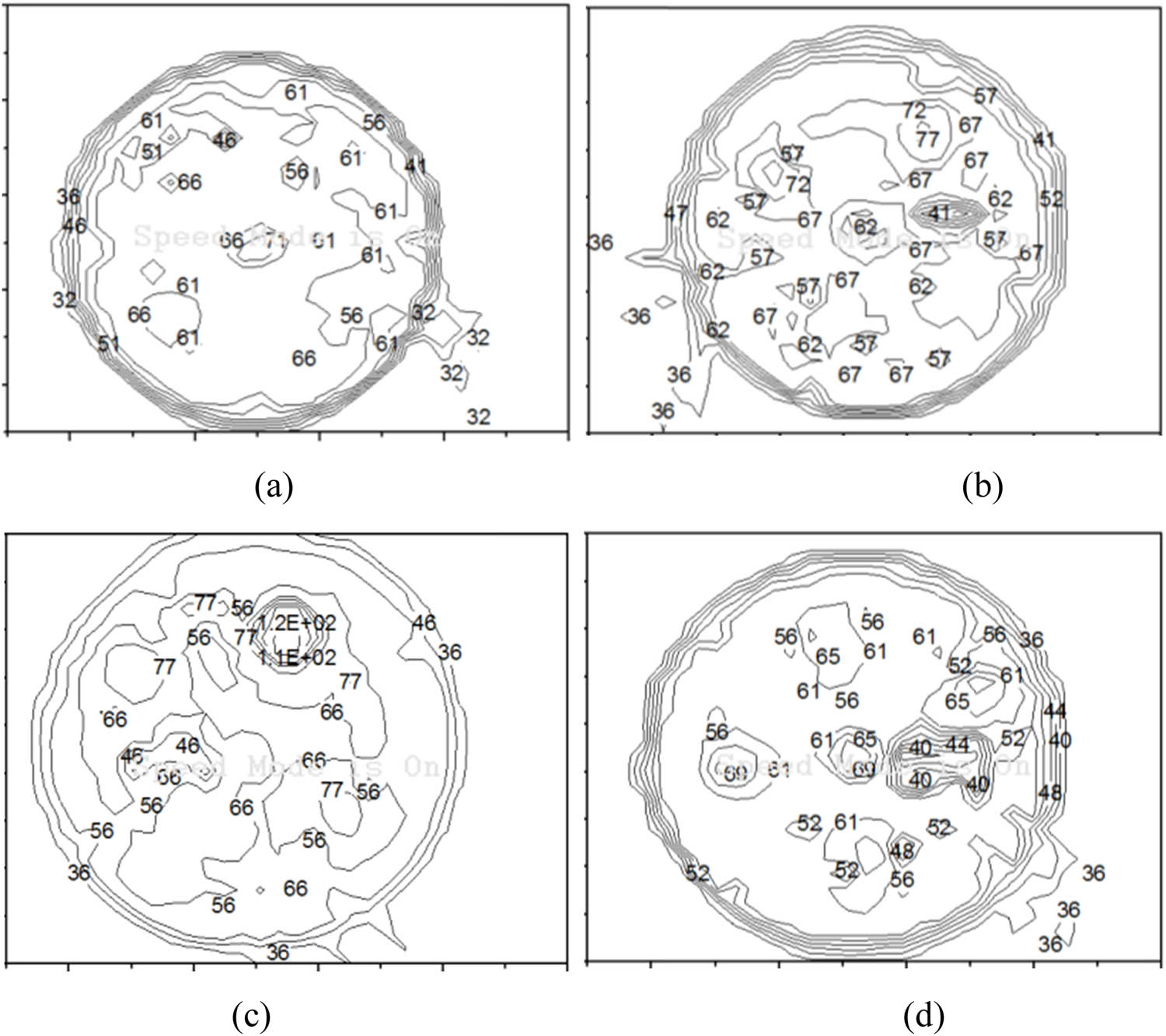
An Isotherm plot of the junction temperature for the LED module at 700 mA when the cooling time of the LED module reaches 60 min for various factors and levels: (a) trial 1, (b) trial 2, (c) trial 13, and (d) trial 16.
4.5 Verification experiments
The confirmation experiments on the optimal factor settings are typically required to verify that the obtained outcomes are consistent with the analytical results according to equation (5). Specifically, it verifies that the results of the experiments that are obtained with the best parameters actually provide the expected findings. In this study, a set of confirmation tests were conducted and the thermal dissipation structure module was successfully constructed and a series of tests were made. In addition, the improved % variation,
That is, by increasing the SN ratio by 6 dB, the variance is reduced to half of the original. Thus, a gain of 1.30 dB corresponds to a 9.67% reduction in variance, which indicates the improvement through the optimal setting by 1.162 times variance. Also, the histogram of the S/N ratio in Figure 6 shows the predicted values and the comparison with the actual values, which suggests that the predicted and actual values are reasonably similar using the additive method. As seen earlier, the predicted 0.23 dB is very close to the actual gain of 1.30 dB. This indicates that the optimal setting provides a strong enough resistance to the effects of noise and leads to high reproducibility.
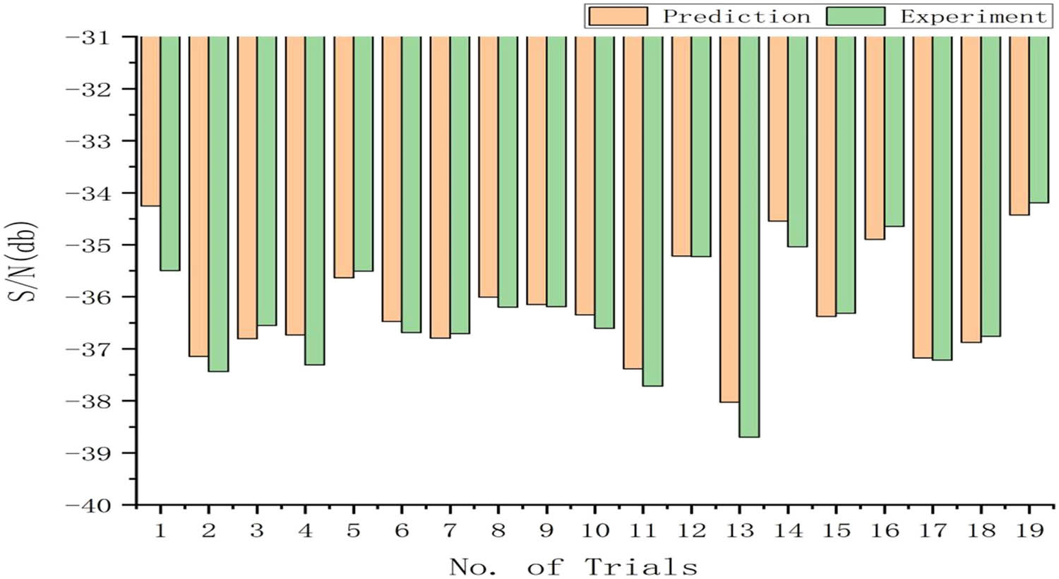
Comparison of predicted and actual values based on additive method.
In order to confirm the validity of the resulting values obtained by optimizing the control factors and to provide a good understanding of the performance of the junction temperature of the Cu2O coating mounted on the heat sink, a visual representation of the optimized heat sink structure is shown in Figure 7. The optimal factorial-level results of the junction temperature of the structure of the LED module based on Taguchi design are a vertical groove (A2), the number of groove is 10 (B3), the width of the groove is 3 mm (C3), the depth of the groove is 3 mm (D3), two heat dissipation holes are drilled neighbor to each other (E2), the heat dissipation cream coefficient is 4.6 W·m−1·K−1 (F3), the LED is a combination of 5W × 5W × 1W × 1W (G1), and there is no bump (H1) as shown in Figure 7a and b, which is the best factors based on the average analysis of response and an ANOVA as shown in Tables 3 and 4. Notably, the optimal factor of Test 19 in Figure 7 still yields the best S/N ratio of −34.20 dB when compared with Test 13 in Table 3, which has the highest S/N ratio of −34.65 dB. That is, the average temperature of 51.26°C in Figure 7c and d is more favorable than that of 54.0°C in Test 13 in Table 3. This shows that the quality characteristics obtained through the optimal setting of factors can be obtained robustly and result in well reproducible.
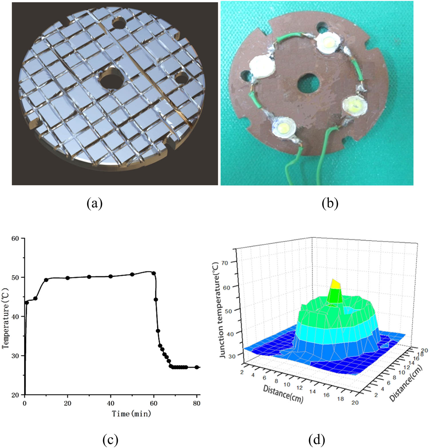
The confirm run of the optimal control factors and levels (a) 10 vertical grooves, (b) a 5W-5W-1W-1W module mounted on Cu2O-coated heat sink structure, (c) the temperature distribution of linear graphs, and (d) the temperature distribution of 3D graphs.
Response table of SN on the junction temperature with various control factors and their levels
| SN | A | B | C | D | E | F | G | H |
|---|---|---|---|---|---|---|---|---|
| Level 1 | −36.46 | −36.40 | −36.58 | −36.60 | −36.29 | −36.59 | −35.35 | −36.15 |
| Level 2 | −36.40 | −36.60 | −36.41 | −36.73 | −36.19 | −36.56 | −36.83 | −36.79 |
| Level 3 | 0.00 | −36.29 | −36.29 | −35.96 | −36.80 | −36.13 | −37.10 | −36.34 |
| Effect | 0.06 | 0.31 | 0.29 | 0.77 | 0.60 | 0.46 | 1.74 | 0.64 |
| Rank | 8 | 6 | 7 | 2 | 4 | 5 | 1 | 3 |
An ANOVA for the junction temperature based on the Taguchi design
| Control factors | Sum of squares | Degree of freedom | Variance | F-Value | Contribution percent |
|---|---|---|---|---|---|
| A | 0.016 | 1.0 | 0.016 | 0.246 | 0.10 |
| B | 0.291 | 2.0 | 0.145 | 2.195 | 1.75 |
| C | 0.253 | 2.0 | 0.126 | 1.906 | 1.52 |
| D | 2.042 | 2.0 | 1.021 | 15.405 | 12.28 |
| E | 1.259 | 2.0 | 0.629 | 9.495 | 7.57 |
| F | 0.794 | 2.0 | 0.397 | 5.986 | 4.77 |
| G | 10.569 | 2.0 | 5.284 | 79.729 | 63.56 |
| H | 1.273 | 2.0 | 0.636 | 9.600 | 7.65 |
| Error | 0.133 | 2.0 | 0.066 | 1.000 | 0.80 |
| Total | 16.628 | 17.0 | 0.978 | — | 100.00 |
Furthermore, for Figure 8, the temperature curves were plotted over a period of 60 min by optimizing the heat sink with Cu2O coating on the aluminum substrate at drive currents of 100, 200, and 350 mA. A comparison of the temperature curves for different currents reveals that as the time increased from 0 to 60 min at 100, 200, and 350 mA, the temperatures remained around 50, 51, and 41°C, respectively. For further comparison, the junction temperature for the two different current values of 200 and 350 mA at time around 60 min, the temperature was close to around 50°C and did not drastically vary with the increase of time. It is clear that in this experiment, when the current level is below 200 mA, the temperature curve increases with the increase of current. However, between 200 and 350 mA, the temperature profile tends to be stable. It can be predicted from the graph that the temperature curve at 350 mA is not sensitive to time. In total, it is evident that the temperature of the LED module is markedly reduced by the optimization of the heat sink of the Al substrate that is coated with Cu2O. It was found that the optimal heat sink structure with Cu2O-coated Al substrate could yield lower junction temperature values and further improve the thermal performance of the LEDs. Overall, validation tests were improved after optimization, and a satisfactory result was obtained.
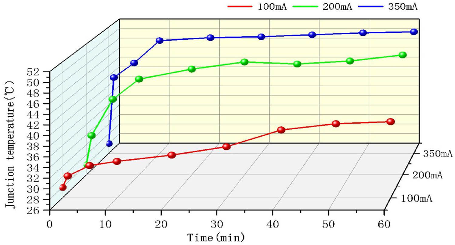
The junction temperature curves of the LEDs over 60 min at currents of 100, 200, and 350 mA by optimizing the heat sink of the aluminum substrate.
5 Conclusions
In this study, the thermal performance of 12W LEDs was investigated by electrostatic Cu2O coatings based on Al substrate heat sink structures according to Taguchi experiments. The influence of the control factors on the junction temperature of the LED module was further discussed. The Ave. R ja values are 3.5 and 3.75°C·W−1, respectively. It can be seen that the R ja values of parallel substrates are not significant compared to those of vertical substrates. This may be due to the solid–air interface defect in the crystal structure, which increases the air contact area, resulting in a lower heat transfer coefficient and thus affecting the heat transfer. Using Taguchi’s method, the most important factors which influence the junction temperature can be obtained. These significant factors constituted approximately 91.06% of the variation in the experiment. Meanwhile, the error of the significant factors contributed about 0.8% to the total variance, which demonstrated that the experiment was considerably effective and the findings were reliable. Through the optimization of significant control factors according to an ANOVA, the junction temperature in the optimal structure of Cu2O-coated heat sink can be optimized. Microstructural examination of Cu2O coating by electrostatic spraying showed few micro mounds, less voids and valleys, and little surface roughness. In addition, the efficiency of the measured junction temperature of the 12W LED module is improved by 23.88% through optimization when compared to the average value of the overall experiments. Also, a gain of 1.30 dB corresponds to a 9.67% reduction in variance, which indicates the improvement through the optimal setting by 1.162 times of variance. Evidently, the heat dissipation results after the optimization of the heat sink module proved to be greatly improved, and these findings were verified in terms of junction temperature. Overall, it shows that the experiment was fairly successful results, demonstrating an excellent reproducibility.
Acknowledgments
The authors gratefully acknowledge financial support from the Project of Science and Technology Department of Fujian Province(No. KL5022006), Project of Educational Teaching Reform of Fujian Province(No. C150825),Undergraduate Education and Teaching Reform Research Project of Fujian Province (No. FBJG20220194).
-
Funding information: This work was supported by the Project of Science and Technology Department of Fujian Province(KL5022006), Project of Educational Teaching Reform of Fujian Province(C150825),Undergraduate Education and Teaching Reform Research Project of Fujian Province FBJG20220194).
-
Author contributions: Congrong Wang: Research, revision, funding; Mingder Jean: Writing and graphics; Chaoyang Zhang: Experiment and data; Hui Lin: Conception of the study and manuscript preparation; Xinting Sun: Manuscript preparation; Jiahao Li: Calculation and data; Qiduan Chen: Revision.
-
Conflict of interest: Authors state no conflict of interest.
-
Data availability statement: All authors can confirm that all data used in this article can be published the Journal “High Temperature Materials and Processes”.
References
[1] Wang, J., M. Ijaz Khan, W. A. Khan, S. Z. Abbas, and M. Imran Khan. Heat transfer performance of a novel tubular oscillating heat pipe with sintered copper particles inside flat-plate evaporator and high-power LED heat sink application. Energy Conversion and Management, Vol. 189, 2019, pp. 215–222.10.1016/j.enconman.2019.03.093Search in Google Scholar
[2] Tang, Y., Y. Luo, P. Du, H. Wang, H. Ma, Y. Qin, et al. Experimental investigation on active heat sink with heat pipe assistance for high-power automotive LED headlights. Case Studies in Thermal Engineering, Vol. 28, 2021, id. 101503.10.1016/j.csite.2021.101503Search in Google Scholar
[3] Yang, C., X. Hou, and S. Chang. A synchronous placement and size-based multi-objective optimization method for heat dissipation design on antenna module of space solar power satellite. Sustainable Energy Technologies and Assessments, Vol. 45, 2021, id. 101183.10.1016/j.seta.2021.101183Search in Google Scholar
[4] Hamidnia, M., Y. Luo, and X. D. Wang. Application of micro/nano technology for thermal management of high power LED packaging–A review. Applied Thermal Engineering, Vol. 145, 2018, pp. 637–651.10.1016/j.applthermaleng.2018.09.078Search in Google Scholar
[5] Paniagua-Guerra, L. E., S. Sehgal, C. U. Gonzalez-Valle, and B. Ramos-Alvarado. Fractal channel manifolds for microjet liquid-cooled heat sinks. International Journal of Heat and Mass Transfer, Vol. 138, 2019, pp. 257–266.10.1016/j.ijheatmasstransfer.2019.04.039Search in Google Scholar
[6] Liang, S., R. Hao, D. Fan, B. Li, J. Huang, Y. Zhang, et al. Structural optimization and numerical thermal analysis of ultraviolet light-emitting diodes with high-power multi-chip arrays. Optik, Vol. 222, 2020, id. 165333.10.1016/j.ijleo.2020.165333Search in Google Scholar
[7] Şevik, S., M. Abuşka, and Ö. Özdilli. Thermal performance analysis of a novel linear LED housing with inner and outer fins. International Communications in Heat and Mass Transfer, Vol. 119, 2020, id. 104970.10.1016/j.icheatmasstransfer.2020.104970Search in Google Scholar
[8] Yu, Y., L. L. Ma, W. Y. Huang, J. L. Li, P. K. Wong, and J. C. Yu. Coating MWNTs with Cu2O of different morphology by a polyol process. Journal of Solid State Chemistry, Vol. 178, No. 5, 2005, pp. 1488–1494.10.1016/j.jssc.2005.02.016Search in Google Scholar
[9] Bera, S. C., R. V. Singh, and V. K. Garg. Temperature behavior and compensation of light-emitting diode. IEEE Photonics Technology Letters, Vol. 17, No. 11, 2005, pp. 2286–2288.10.1109/LPT.2005.858154Search in Google Scholar
[10] Shatalov, M., A. Chitnis, P. Yadav, M. F. Hasan, J. Khan, V. Adivarahan, et al. Thermal analysis of flip-chip packaged 280 nm nitride-based deep ultraviolet light-emitting diodes. Applied Physics Letters, Vol. 86, No. 20, 2005, id. 201109.10.1063/1.1927695Search in Google Scholar
[11] Arik, M., C. A. Becker, S. E. Weaver, and J. Petroski. Thermal management of LEDs: package to system. Third International Conference on Solid State Lighting, Vol. 5187, SPIE, 2004, pp. 64–75.10.1117/12.512731Search in Google Scholar
[12] Arik, M., and S. Weaver. Chip-scale thermal management of high-brightness LED packages. Fourth International Conference on Solid State Lighting, Vol. 5530, SPIE, 2004, pp. 214–223.10.1117/12.566061Search in Google Scholar
[13] Ngo, I. L., H. Jang, C. Byon, and B. J. Lee. Experimental study on thermal performance of SMD-LED chips under the effects of electric wire pattern and LED arrangement. International Journal of Heat and Mass Transfer, Vol. 127, 2018, pp. 746–757.10.1016/j.ijheatmasstransfer.2018.08.089Search in Google Scholar
[14] Sui, G., J. Chen, H. Ni, Y. Ma, X. Gao, and N. Wang. Improvement of LED performance with an integrated thermoelectric cooling package. IEEE Access, Vol. 8, 2020, pp. 116535–116543.10.1109/ACCESS.2020.3004142Search in Google Scholar
[15] Ghrib, T., N. K. AL-Saleem, A. Al-Naghmaish, A. A. Elshekhipy, S. Brini, K. Briki, et al. Annealing effect on the microstructural, optical, electrical, and thermal properties of Cu2O/TiO2/Cu2O/TiO2/Si heterojunction prepared by sol-gel technique. Micro and Nanostructures, Vol. 164, 2022, id. 107119.10.1016/j.spmi.2021.107119Search in Google Scholar
[16] Wei, X., H. Zhu, T. Kong, and L. Wang. Synthesis and thermal conductivity of Cu2O nanofluids. International Journal of Heat and Mass Transfer, Vol. 52, No. 19–20, 2009, pp. 4371–4374.10.1016/j.ijheatmasstransfer.2009.03.073Search in Google Scholar
[17] Borgohain, K., N. Murase, and S. Mahamuni. Synthesis and properties of Cu2O quantum particles. Journal of Applied Physics, Vol. 92, No. 3, 2002, pp. 1292–1297.10.1063/1.1491020Search in Google Scholar
[18] Zhang, L. and H. Wang. Cuprous oxide nanoshells with geometrically tunable optical properties. ACS Nano, Vol. 5, No. 4, 2011, pp. 3257–3267.10.1021/nn200386nSearch in Google Scholar PubMed
[19] Xu, L., L. P. Jiang, and J. J. Zhu. Sonochemical synthesis and photocatalysis of porous Cu2O nanospheres with controllable structures. Nanotechnology, Vol. 20, No. 4, 2008, id. 045605.10.1088/0957-4484/20/4/045605Search in Google Scholar PubMed
[20] Wu, W., W. Zhao, Y. Wu, C. Zhou, L. Li, Z. Liu, et al. Antibacterial behaviors of Cu2O particles with controllable morphologies in acrylic coatings. Applied Surface Science, Vol. 465, 2019, pp. 279–287.10.1016/j.apsusc.2018.09.184Search in Google Scholar
[21] Park, J., M. Shin, and C. C. Lee. Measurement of temperature profiles on visible light-emitting diodes by use of a nematic liquid crystal and an infrared laser. Optics letters, Vol. 29, No. 22, 2004, pp. 2656–2658.10.1364/OL.29.002656Search in Google Scholar PubMed
[22] Petroski, J. Spacing of high-brightness LEDs on metal substrate PCB’s for proper thermal performance. The Ninth Intersociety Conference on Thermal and Thermomechanical Phenomena In Electronic Systems (IEEE Cat. No. 04CH37543), Vol. 2, IEEE, 2004, pp. 507–514.10.1109/ITHERM.2004.1318326Search in Google Scholar
[23] Yin, L., L. Yang, W. Yang, Y. Guo, K. Ma, S. Li, et al. Thermal design and analysis of multi-chip LED module with ceramic substrate. Solid-State Electronics, Vol. 54, No. 12, 2010, pp. 1520–1524.10.1016/j.sse.2010.06.028Search in Google Scholar
[24] Anithambigai, P., K. Dinash, D. Mutharasu, S. Shanmugan, and C. K. Lim. Thermal analysis of power LED employing dual interface method and water flow as a cooling system. Thermochimica Acta, Vol. 523, No. 1–2, 2011, pp. 237–244.10.1016/j.tca.2011.06.001Search in Google Scholar
[25] Parbrook, P. J., B. Corbett, J. Han, T. Y. Seong, and H. Amano. Micro‐light emitting diode: from chips to applications. Laser & Photonics Reviews, Vol. 15, No. 5, 2021, id. 2000133.10.1002/lpor.202000133Search in Google Scholar
[26] Rammohan, A. and V. P. Chandramohan. Experimental analysis on estimating junction temperature and service life of high power LED array. Microelectronics Reliability, Vol. 120, 2021, id. 114121.10.1016/j.microrel.2021.114121Search in Google Scholar
[27] Liu, C. C., M. T. Sheen, and S. F. Wang. Optimal design of heat dissipation modules for high-power LED based on the Taguchi method. Thermal Science, Vol. 27(1A), 2023, pp. 219–231.10.2298/TSCI220329124LSearch in Google Scholar
[28] Feng, S., Z. Liu, B. Cheng, S. Sun, T. J. Lu, and F. Xu. Design of a novel LED bulb with entire surface thermally activated for passive cooling. Applied Thermal Engineering, Vol. 198, 2021, id. 117466.10.1016/j.applthermaleng.2021.117466Search in Google Scholar
[29] Gatapova, E. Y., G. Sahu, S. Khandekar, and R. Hu. Thermal management of high-power LED module with single-phase liquid jet array. Applied Thermal Engineering, Vol. 184, 2021, id. 116270.10.1016/j.applthermaleng.2020.116270Search in Google Scholar
[30] Khandekar, S., G. Sahu, K. Muralidhar, E. Y. Gatapova, O. A. Kabov, R. Hu, et al. Cooling of high-power LEDs by liquid sprays: Challenges and prospects. Applied Thermal Engineering, Vol. 184, 2021, id. 115640.10.1016/j.applthermaleng.2020.115640Search in Google Scholar
[31] Wang, J. B., X. H. Li, J. Wang, T. Zhu, and Y. C. Bao. Thermal performance evaluation of a thermoelectric cooler coupled with corona wind. Applied Thermal Engineering, Vol. 179, 2020, id. 115753.10.1016/j.applthermaleng.2020.115753Search in Google Scholar
[32] Peng, X., S. Li, Z. Liu, B. Zhang, Y. Peng, D. Yu, et al. Highly thermal conductive red-emitting AlN-CaAlSiN3: Eu2 + composite phosphor ceramics for high-power laser-driven lighting. Journal of the European Ceramic Society, Vol. 41, No. 11, 2021, pp. 5650–5657.10.1016/j.jeurceramsoc.2021.03.066Search in Google Scholar
[33] Zou, C., Y. Liu, D. S. Ginger, and L. Y. Lin. Suppressing efficiency roll-off at high current densities for ultra-bright green perovskite light-emitting diodes. ACS Nano, Vol. 14, No. 5, 2020, pp. 6076–6086.10.1021/acsnano.0c01817Search in Google Scholar PubMed
[34] Kumar, P., G. Sahu, D. Chatterjee, and S. Khandekar. Copper wick based loop heat pipe for thermal management of a high-power LED module. Applied Thermal Engineering, Vol. 211, 2022, id. 118459.10.1016/j.applthermaleng.2022.118459Search in Google Scholar
[35] Ross, P. J. Taguchi techniques for quality engineering, 2nd edn, McGraw-Hill, New York, 1995.Search in Google Scholar
[36] Myers, R. H., D. C. Montgomery, and C. M. Anderson-Cook. Response surface methodology: Process and product optimization using designed experiments, 3rd edn, John Wiley & Sons, Inc, Hoboken, New Jersey, 2009.Search in Google Scholar
[37] Zheng, Z., J. Dai, Y. Zhang, H. Wang, A. Wang, M. Shan, et al. Enhanced heat dissipation of phosphor film in WLEDs by AlN-coated sapphire plate. IEEE Transactions on Electron Devices, Vol. 67, No. 8, 2020, pp. 3180–3185.10.1109/TED.2020.2997758Search in Google Scholar
[38] Mou, Y., Z. Yu, Z. Lei, M. Chen, and Y. Peng. Enhancing opto-thermal performances of white laser lighting by high reflective phosphor converter. Journal of Alloys and Compounds, Vol. 918, 2022, id. 165637.10.1016/j.jallcom.2022.165637Search in Google Scholar
[39] Zhou, F., G. Zhou, J. Zhou, X. Huai, Y. Jiang, and Q. Huang. Thermal performance evaluation of a novel ultra-thin vapor chamber with Laval-like nozzle composite wick under different air cooling conditions. Case Studies in Thermal Engineering, Vol. 31, 2022, id. 101845.10.1016/j.csite.2022.101845Search in Google Scholar
[40] Mou, Y., H. Wang, Y. Peng, H. Cheng, Q. Sun, and M. Chen. Enhanced heat dissipation of high-power light-emitting diodes by Cu nanoparticle paste. IEEE Electron Device Letters, Vol. 40, No. 6, 2019, pp. 949–952.10.1109/LED.2019.2912458Search in Google Scholar
[41] Xu, Z. Thermal performance and multi-objective optimization of thermosyphon heat sinks with rectangular radial fins for high power LED lamps cooling. Case Studies in Thermal Engineering, Vol. 30, 2022, id. 101778.10.1016/j.csite.2022.101778Search in Google Scholar
[42] Huang, J., W. Zhou, J. Xiang, C. Liu, Y. Gao, S. Li, et al. Development of novel flexible heat pipe with multistage design inspired by structure of human spine. Applied Thermal Engineering, Vol. 175, 2020, id. 115392.10.1016/j.applthermaleng.2020.115392Search in Google Scholar
[43] Huang, J., J. Xiang, X. Chu, W. Sun, R. Liu, W. Ling, et al. Thermal performance of flexible branch heat pipe. Applied Thermal Engineering, Vol. 186, 2021, id. 116532.10.1016/j.applthermaleng.2020.116532Search in Google Scholar
[44] Peng, Y., Z. Yu, J. Zhao, Q. Wang, J. Liu, B. Sun, et al. Unique sandwich design of high-efficiency heat-conducting phosphor-in-glass film for high-quality laser-driven white lighting. Journal of Advanced Ceramics, Vol. 11, No. 12, 2022, pp. 1889–1900.10.1007/s40145-022-0654-7Search in Google Scholar
[45] Li, Y. H., Y. K. Zhao, and H. Q. Chen. Prediction model of interfacial heat transfer coefficient changing with time and ingot diameter. High Temperature Materials and Processes, Vol. 41, 2022, pp. 238–246.10.1515/htmp-2022-0008Search in Google Scholar
© 2023 the author(s), published by De Gruyter
This work is licensed under the Creative Commons Attribution 4.0 International License.
Articles in the same Issue
- Research Articles
- First-principles investigation of phase stability and elastic properties of Laves phase TaCr2 by ruthenium alloying
- Improvement and prediction on high temperature melting characteristics of coal ash
- First-principles calculations to investigate the thermal response of the ZrC(1−x)Nx ceramics at extreme conditions
- Study on the cladding path during the solidification process of multi-layer cladding of large steel ingots
- Thermodynamic analysis of vanadium distribution behavior in blast furnaces and basic oxygen furnaces
- Comparison of data-driven prediction methods for comprehensive coke ratio of blast furnace
- Effect of different isothermal times on the microstructure and mechanical properties of high-strength rebar
- Analysis of the evolution law of oxide inclusions in U75V heavy rail steel during the LF–RH refining process
- Simultaneous extraction of uranium and niobium from a low-grade natural betafite ore
- Transfer and transformation mechanism of chromium in stainless steel slag in pedosphere
- Effect of tool traverse speed on joint line remnant and mechanical properties of friction stir welded 2195-T8 Al–Li alloy joints
- Technology and analysis of 08Cr9W3Co3VNbCuBN steel large diameter thick wall pipe welding process
- Influence of shielding gas on machining and wear aspects of AISI 310–AISI 2205 dissimilar stainless steel joints
- Effect of post-weld heat treatment on 6156 aluminum alloy joint formed by electron beam welding
- Ash melting behavior and mechanism of high-calcium bituminous coal in the process of blast furnace pulverized coal injection
- Effect of high temperature tempering on the phase composition and structure of steelmaking slag
- Numerical simulation of shrinkage porosity defect in billet continuous casting
- Influence of submerged entry nozzle on funnel mold surface velocity
- Effect of cold-rolling deformation and rare earth yttrium on microstructure and texture of oriented silicon steel
- Investigation of microstructure, machinability, and mechanical properties of new-generation hybrid lead-free brass alloys
- Soft sensor method of multimode BOF steelmaking endpoint carbon content and temperature based on vMF-WSAE dynamic deep learning
- Mechanical properties and nugget evolution in resistance spot welding of Zn–Al–Mg galvanized DC51D steel
- Research on the behaviour and mechanism of void welding based on multiple scales
- Preparation of CaO–SiO2–Al2O3 inorganic fibers from melting-separated red mud
- Study on diffusion kinetics of chromium and nickel electrochemical co-deposition in a NaCl–KCl–NaF–Cr2O3–NiO molten salt
- Enhancing the efficiency of polytetrafluoroethylene-modified silica hydrosols coated solar panels by using artificial neural network and response surface methodology
- High-temperature corrosion behaviours of nickel–iron-based alloys with different molybdenum and tungsten contents in a coal ash/flue gas environment
- Characteristics and purification of Himalayan salt by high temperature melting
- Temperature uniformity optimization with power-frequency coordinated variation in multi-source microwave based on sequential quadratic programming
- A novel method for CO2 injection direct smelting vanadium steel: Dephosphorization and vanadium retention
- A study of the void surface healing mechanism in 316LN steel
- Effect of chemical composition and heat treatment on intergranular corrosion and strength of AlMgSiCu alloys
- Soft sensor method for endpoint carbon content and temperature of BOF based on multi-cluster dynamic adaptive selection ensemble learning
- Evaluating thermal properties and activation energy of phthalonitrile using sulfur-containing curing agents
- Investigation of the liquidus temperature calculation method for medium manganese steel
- High-temperature corrosion model of Incoloy 800H alloy connected with Ni-201 in MgCl2–KCl heat transfer fluid
- Investigation of the microstructure and mechanical properties of Mg–Al–Zn alloy joints formed by different laser welding processes
- Effect of refining slag compositions on its melting property and desulphurization
- Effect of P and Ti on the agglomeration behavior of Al2O3 inclusions in Fe–P–Ti alloys
- Cation-doping effects on the conductivities of the mayenite Ca12Al14O33
- Modification of Al2O3 inclusions in SWRH82B steel by La/Y rare-earth element treatment
- Possibility of metallic cobalt formation in the oxide scale during high-temperature oxidation of Co-27Cr-6Mo alloy in air
- Multi-source microwave heating temperature uniformity study based on adaptive dynamic programming
- Round-robin measurement of surface tension of high-temperature liquid platinum free of oxygen adsorption by oscillating droplet method using levitation techniques
- High-temperature production of AlN in Mg alloys with ammonia gas
- Review Article
- Advances in ultrasonic welding of lightweight alloys: A review
- Topical Issue on High-temperature Phase Change Materials for Energy Storage
- Compositional and thermophysical study of Al–Si- and Zn–Al–Mg-based eutectic alloys for latent heat storage
- Corrosion behavior of a Co−Cr−Mo−Si alloy in pure Al and Al−Si melt
- Al–Si–Fe alloy-based phase change material for high-temperature thermal energy storage
- Density and surface tension measurements of molten Al–Si based alloys
- Graphite crucible interaction with Fe–Si–B phase change material in pilot-scale experiments
- Topical Issue on Nuclear Energy Application Materials
- Dry synthesis of brannerite (UTi2O6) by mechanochemical treatment
- Special Issue on Polymer and Composite Materials (PCM) and Graphene and Novel Nanomaterials - Part I
- Heat management of LED-based Cu2O deposits on the optimal structure of heat sink
- Special Issue on Recent Developments in 3D Printed Carbon Materials - Part I
- Porous metal foam flow field and heat evaluation in PEMFC: A review
- Special Issue on Advancements in Solar Energy Technologies and Systems
- Research on electric energy measurement system based on intelligent sensor data in artificial intelligence environment
- Study of photovoltaic integrated prefabricated components for assembled buildings based on sensing technology supported by solar energy
- Topical Issue on Focus of Hot Deformation of Metaland High Entropy Alloys - Part I
- Performance optimization and investigation of metal-cored filler wires for high-strength steel during gas metal arc welding
- Three-dimensional transient heat transfer analysis of micro-plasma arc welding process using volumetric heat source models