Shock and impact reliability of electronic assemblies with perimeter vs full array layouts: A numerical comparative study
-
Mohammad A. Gharaibeh


Abstract
This study aims to assess the effect of the solder joint array layouts, including full and peripheral designs, on the mechanical response and reliability of electronic packages subjected to shock and impact loadings. Linear and nonlinear finite element simulations using the global-local modeling technique are employed to perform the analysis. Several peripheral array configurations are considered and compared to the full array systems. The results showed that, for optimum electronic package designs in terms of reliability and cost, it is highly recommended to use peripheral packages having three or four rows of solder interconnects in electronic systems under shock and impact loadings.
1 Introduction
Ball grid array (BGA) solder technologies are rapidly becoming of popular interest in designing electronic devices due to its cost-efficient properties [1,2], smaller size [3] and high input/output (I/O) electrical characteristics [4,5]. In fact, BGAs are commonly categorized based on the solder shape, i.e., geometry, and array layout [6]. Actually, BGA reliability is highly dependent on the geometric factors of the joint, i.e., diameter and standoff height [7,8,9]. For the layout configurations, peripheral (or perimeter) and full arrays are the most popular solder array or matrix layouts [10]. Generally, full arrays are available in most BGA component types while the perimeter configuration is widely used in wafer-level packages (WLP) and plastic ball grid array (PBGA) components [11]. Only a few published works are available for the reliability assessment of full vs peripheral array layouts. Using the finite element (FE) simulations, Chandran et al. [12] identified the location of solders with maximum damage to be at the package corner in both peripheral and full arrays in accelerated thermal cycling testing. In addition, their results showed that the risk of solder thermal fatigue is much possible in peripheral arrays than full array configurations. Such findings were recently confirmed with Gharaibeh’s simulation-based work [13]. Liu et al. [14] used FE models to enhance the thermal reliability of peripheral WLP systems by installing dummy solder interconnects of larger sizes (height and diameter) at the array corner and around the corner. Titus and Jaiswal [15] discussed the reliability of solder balls of several arrangements of array designs considering different I/O counts. They found that the package with larger I/O count number could generally improve the solder interconnect thermal cycling reliability. However, BGA packages with high I/O counts and small pitch distance (distance between two adjacent joints) might lead to routing defects between the solders. Jung et al. [16] used two-dimensional (2-D) FE models to investigate the thermal fatigue characteristics of lead-based solders in both perimeter and full PBGA components. Their results showed that the full array layout systems could last longer than peripheral arrays. However, their results were based on FE numerical models with coarse mesh characteristics and the important and crucial in-plane deformations of the test package were not considered due to the use of 2-D models. Recently, Gharaibeh [17] discussed the random vibration reliability of perimeter and full BGA layouts using comprehensive nonlinear FE analysis. Gharaibeh’s findings stated that in both array arrangements, the location of the critical solder joint is at the corner of the solder matrix. In addition, the value and the distributions of the critical solder stresses are not affected by the array type. Thus, the random vibration reliability is not influenced by the array layout. This was explained based on the fact that the outer solder rows/columns of the solder matrix carry most of the bending induced mechanical stresses and loadings while the inner interconnects do not meaningfully contribute to that. However, the use of peripheral arrangements could lead to electrical conductivity problems.
Based on the previous literature discussions, it is proved that most of the work done on the effect of the solder array configuration on electronic package reliability was limited to the thermal cycling and vibration loading conditions. Evidently, there is a lack of research studies investigating the behavior of full and peripheral solder layouts in drop, shock and impact loadings. Therefore, this article aims to bridge this research gap and discuss the mechanical behavior and reliability of electronic packages with both peripheral and full array configurations due to shock and impact loadings using computationally effective nonlinear finite element analysis (FEA) models with high-quality mesh properties.
This article begins with a detailed description of the package array layouts studied as well as the test assembly considered. Consequently, the FE modeling approach and global-local analysis techniques are fully presented. The correlations of the present FE models with modal analysis with hammer testing experiments are discussed, accordingly. Subsequently, a comprehensive presentation of the effect of solder matrix layout on the impact-induced mechanical behavior is explored. Finally, the present work provides useful design recommendations of BGA electronic packages exposed to shock and impact loadings.
2 Methodology
2.1 Area array layouts
In the present work, an integrated circuit (IC) package with body size of 17 mm2 × 17 mm2 and

Solder array layouts:
Test configurations details
| Part | Configuration |
|---|---|
| PCB size (
|
|
| PCB thickness (
|
|
| Component size (
|
|
| Component thickness (
|
1 |
| IC Package |
|
| I/O count | Full: 256, peripheral: 192 |
| Solder joint type | BGA |
| Solder joint alloy |
|
| Solder joint height and diameter (
|
|
| Pitch distance (
|
1 |
2.2 FE modeling
ANSYS R17.1 is considered to build the FE model and to analyze the problem. For the FE mesh process in this model, only 3-dimensional hexahedron SOLID185 elements are generated to produce high-quality mapped mesh properties. During the modeling, only linear elastic mechanical properties are employed for the PCB, IC component and copper pads. However, for the SAC305 metallic alloy, both linear and nonlinear mechanical properties are considered. For the nonlinear material modeling, Anand visco-plastic constitutive material model [18,19] is implemented. All material properties are listed in listed in Tables 2 and 3. For the boundary conditions and to properly restrain the FE model, zero translational and rotational motions are imposed on the four corners of the PCB. This FE model is presented in Figure 2.
| Material Parameter | PCB | Component | SAC305 | Copper pads |
|---|---|---|---|---|
| Young’s modulus
|
32.0 | 27.0 | 43.0 | 120.0 |
| Poisson’s ratio | 0.24 | 0.25 | 0.36 | 0.30 |
| Density
|
3,000 | 1,100 | 7,400 | 8,800 |
Anand model parameters used in the FE model for the SAC305 solder alloy [23]
| Anand’s parameter | Description | Units | SAC305 |
|---|---|---|---|
|
|
Initial value of deformation resistance |
|
32.2 |
|
|
Activation energy/Boltzmann’s constant |
|
9,320 |
|
|
Pre-exponential factor |
|
2,800 |
|
|
Stress multiplier | Dimensionless | 4 |
|
|
Strain rate sensitivity of stress | Dimensionless | 0.29 |
|
|
Hardening-softening constant |
|
186,000 |
|
|
Coefficient for saturation value of deformation resistance |
|
44.67 |
|
|
Strain rate sensitivity of the saturation value | Dimensionless | 0.0120 |
|
|
Strain rate sensitivity of the Hardening-softening | Dimensionless | 1.72 |

Finite element model.
In impact loadings, the electronic structure undergoes very large deformation and high strains during a very short period of time. In fact, performing nonlinear simulations in impact loading conditions is computationally very expensive in terms of computer run durations and memory as well as hardware resources usage. Nonetheless, it is very important to simulate the large deformations and the nonlinear behavior of the solder interconnect to reasonably estimate stresses and strains of the critical regions of the electronic structure, of course with computationally effective approaches. For this reason, the current study adopts the global-local modeling technique for executing the analysis for best results and for optimum simulation characteristics. This technique generally consists of two steps. In the first step, the global (full) model is executed using the mode superposition transient ANSYS analysis considering only linear mechanical properties for all parts of the electronic assembly. This step aims to simulate the overall deformations of the assembly with shortest simulation times. This is followed by the second and final analysis step in which a local model (submodel) of the most-critical solder interconnect, with improved mesh properties, is analyzed using nonlinear static analysis. The main goal of implementing the submodeling approach here is to generate and simulate an engineered and finely tweaked FE model of the most important solder joint. Figure 3 shows the corner solder joint mesh used in the full (global) model and in the submodel (local) configuration. In this submodel, the mechanical properties of the PCB, IC package and copper pads are remained linear elastic and are the same for the global model. However, the SAC305 solder mechanical properties in the local modeling are nonlinear for best solder stress computations. This is a common practice as it is very well known that the solder properties do not significantly influence the overall stiffness of the test assembly; however, solder stresses are highly dependent on the mechanical properties. If the nonlinear mechanical properties are plugged into the full model, the FEA simulation time will be very long and computationally intensive. Thus, the nonlinearities are only included in the local modeling. As a result, in this global-local modeling process, both accuracy and simulation efficiency are optimized.

Solder joint used in (a) global model and (b) local model.
Internationally, Joint Electron Device Engineering Council (JEDEC) recommends general rules and standards for conducting and simulating the reliability performance of electronic assemblies under shock impact loadings [23,24,25]. One specific JEDEC condition, namely JEDEC B-Condition, is widely used for the evaluation of SAC305 shock reliability performance. Therefore, JEDEC B-condition, which is characterized by a half-sine wave profile of 1,500 g’s shock level with 0.5
2.3 Modal analysis experiment
Like any other numerical approach, the results of this FE model are required to be validated and correlated. Thus, the current FEA model is correlated with modal analysis with hammer testing experimental findings in terms of the basic dynamic characteristics, i.e., natural frequencies and mode shapes. In other words, the free vibration data (natural frequencies and mode shapes) of the FEA model are systemically compared to their corresponding experimental results and hence discrepancies are quantified by the relative error in the resonant frequencies and modal assurance criterion (MAC) number for the mode shapes. Throughout this correlation process, free boundary conditions are considered, and the first five vibratory modes are tested.
For the details of the modal analysis experiment, the setup is composed of an impact hammer (exciter), a data acquisition system (DAQ), a light-weight accelerometer, a computer and the test vehicle. Table 4 lists all the specifications of this setup. For the measurement procedure, a 7-by-7 equally spread-out grid is marked on the test sample. The hammer is accordingly used to softly tap the assembly at each measurement point (total of 49), while the board accelerations are continuously measured using the accelerometer. For more accurate measurement, the average of three consecutive taps is computed and hence considered. Consequently, the transfer function between the output acceleration and the input hammer force is acquired using the DAQ device. Finally, the PUMA V7.2 software from Spectral Dynamics is used for the modal data generation. Figure 4 shows the schematics of the test and a photograph for the actual test piece.
Modal analysis experimental setup details
| Equipment | Make and model number |
|---|---|
| Impulse hammer | PCB Piezoeletronics 086C01 |
| Accelerometer | PCB Piezoeletronics 352C23 |
| DAQ system | National Instruments NI-DAQ 4431 |
| Software | Spectral Dynamics STAR Version 7.2 |

Modal analysis experiment.
The results of this validation analysis, detailed in Tables 5 and 6, show that the FEA natural frequency and mode shapes are in a very good agreement with the corresponding measured data. As a result, the present FE model can be further employed with confident to perform the rest of the analysis in this work.
Natural frequencies correlation results
| Mode number | Experiment natural frequency (
|
FEA natural frequency (
|
% Error |
|---|---|---|---|
| 1 | 422 | 421 | –0.24 |
| 2 | 626 | 636 | 1.60 |
| 3 | 770 | 691 | –10.34 |
| 4 | 1,036 | 993 | –4.25 |
Vibratory mode shapes correlation results
| Mode # | Measured mode shape | FEA mode shape | MAC |
|---|---|---|---|
| 1 |
|

|
0.99 |
| 2 |
|

|
0.97 |
| 3 |

|

|
0.96 |
| 4 |

|

|
0.91 |
3 Results and discussions
3.1 Board deflections
Figure 5 shows the time response of the transverse deformations (U
Z), in both full and perimeter array layouts, at the PCB center due to the applied shock profile. The first conclusion that can be drawn here is that the boards with any array configuration have the same natural frequency as the natural period time is the same for both systems. Another important observation is that the maximum lateral deflection of the PCB is almost the same for both array configurations. Specifically, in full array

Time response of the out-of-plane deflections of the PCB in full and perimeter rray.
3.2 Solder interconnects stress analysis
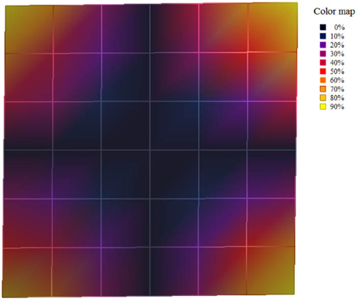
Figure 6 presents the von Mises stress contour plots of the studied configurations. The figure shows that, in both array styles, the corner joint is the joint with highest stress value, i.e., the most critical solder interconnect. This is due to the bending difference between the PCB and the IC package is often maximum at the package corners. In addition, the stress contour plots show that the solder stresses of the peripheral array are very similar to the stresses of the corresponding interconnects of the full array system. This is true for both solder stress values and distributions. Such findings suggest that for a 4-row/column perimeter array and the full array layouts, the interconnect matrix type does not affect solder stresses. Therefore, the solder located at the outer rows/columns of the matrix undergoes most of the mechanical loading induced by the drop impact and the solder of the inner columns and rows does not exhibit much of the deformations, as explained in Figure 7. From a financial point of view, the use of peripheral arrays is highly preferable, and it could lead to cheaper electronic assemblies’ designs, as less number of solder interconnects are required. However, the use of partial array systems must not interfere with the electrical properties, i.e., conductivity properties, of the electronic system.

Von Mises stresses of the solder matrix in (a) full and (b) peripheral layouts.

Schematics for (a) nondeformed and (b) deformed electronic package after bending due to vibration.
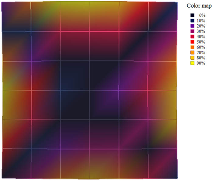
For a closer look on the critical interconnect, i.e., corner joint, the submodel is considered, for both array schemes. Figure 8 presents the von Mises stresses in the critical joints. The plots show that solder stress distributions and values are the same in both peripheral and full array layouts. In addition, the maximum stress in the solder is located at the top (component side). Therefore, the solder mechanical failure due to impact loadings is expected to be the same in both array systems and this failure is more likely to occur at the component side of the outer most interconnect.

Critical solder joints von Mises stress distributions in (a) full and (b) peripheral arrays.
For deeper analysis and understanding of the difference between solder failure in full and perimeter array configurations, an additional FEA investigations are performed. In these investigations, a peripheral array component with four, three, double and single rows (or columns) of the

Von Mises stress distributions of the interconnect array in one-, two-, three- and four-row partial array configurations.

Von Mises stress distributions of the critical solder interconnect in one-, two-, three- and four-row partial array configurations.
Table 7 lists the maximum von Mises stress values of all tested partial array configurations. The results here show that solder stresses are higher for the single row system (
Solder maximum von Mises stress results in several row configurations
| Number of rows in the partial array | von Mises stress (MPa) |
|---|---|
| 1 | 26.1 |
| 2 | 24.7 |
| 3 | 22.3 |
| 4 | 22.3 |
This phenomenon can be justified again using Figure 7. Considering the deformed shape of this figure, the explanation is that the outer rows/columns of the solder ball array do the heavy lifting of the bending-induced mechanical loading while the inner most interconnects do not effectively participate in the loading carrying process. Thus, if the inner joints are not included in (or removed from) the array that would not appreciably affect the outer solders deformations and stresses.
As a result of this discussion, the present work recommends integrated packages with 3- or 4-row/column peripheral arrays designs for cheaper and more dependable electronic structures exposed to shock and impact loadings.
4 Conclusions
Extensive linear and non-linear FE analysis simulations were conducted in the present work to investigate the effect of the solder array layouts, peripheral vs full, on the mechanical behavior and reliability performance of electronic assemblies due to impact and shock loadings. In this investigation, a
-
Funding information: The author states no funding involved.
-
Author contributions: The author has accepted responsibility for the entire content of this manuscript and approved its submission.
-
Conflict of interest: The author states no conflict of interest.
-
Data availability statement: The data that support the findings of this study are available from the corresponding author upon a reasonable request.
References
[1] Borgesen P, Li CY, Conway HD. Mechanical design considerations for area array solder joints. IEEE Trans Components Hybrids Manuf Technol. 1993 May;16(3):272–83.10.1109/33.232053Search in Google Scholar
[2] Lau JH. Ball grid array technology. New York, USA: McGraw-Hill Professional; 1995.Search in Google Scholar
[3] Heinrich SM. Selection of design and process parameters for non-uniform ball grid arrays. Adv Electron Packaging. 1995;1(1):273–88.Search in Google Scholar
[4] Borgesen P, Bolton SC, Yost B, Maggard JG, Brown DD, Li CY. Effects of composition on fatigue crack growth rates in area array solder joints. Adv Electron Packaging. 1993;4(2):969–77.Search in Google Scholar
[5] Marrs RC, Olachea G. BGAs for MCMs. United Kingdom: Advanced Packaging, IHS Publishing Group; 1994 September/October. p. 48–52.Search in Google Scholar
[6] Lasky RC, Singer A, Chouta P. Packaging assembly techniques. Fiber optic data communication: technology advances and futures. 1st ed. Cambridge (MA), USA: Academic Press; 2002 Jan 1. p. 303.10.1016/B978-012207892-7/50009-6Search in Google Scholar
[7] Liu X. Processing and reliability assessment of solder joint interconnection for power chips [dissertation]. Blacksburg, USA: Virginia Polytechnic Institute and State University; 2001.Search in Google Scholar
[8] Liu X, Lu GQ. Effects of solder joint shape and height on thermal fatigue lifetime. IEEE Trans Comp Packaging Technol. 2003 Aug 4;26(2):455–65.10.1109/TCAPT.2003.815089Search in Google Scholar
[9] Lim SS, Rajoo R, Wong EH, Hnin WY. Reliability performance of stretch solder interconnections. 2006 Thirty-First IEEE/CPMT International Electronics Manufacturing Technology Symposium; 2006 Nov 8-10; Petaling Jaya, Malaysia. IEEE; 2008. p. 43–9.10.1109/IEMT.2006.4456430Search in Google Scholar
[10] Gharaibeh MA, Makhlouf AS. Failures of electronic devices: solder joints failure modes, causes and detection methods. In: Hamdy AS, Aliofkhazraei M, editors. Handbook of materials failure analysis. Oxford, UK: Butterworth-Heinemann; 2020 Jan 1. p. 3–17.10.1016/B978-0-08-101937-5.00001-4Search in Google Scholar
[11] Lau CS, Khor CY, Soares D, Teixeira JC, Abdullah MZ. Thermo-mechanical challenges of reflowed lead-free solder joints in surface mount components: a review. Soldering & surface mount technology. UK: Emerald Group Publishing Limited. 2016;28(2):41–62. 10.1108/SSMT-10-2015-0032.Search in Google Scholar
[12] Chandran B, Goyal D, Thomas J. Effect of package design and layout on BGA solder joint reliability of an organic C4 package. In 2000 Proceedings. 50th Electronic Components and Technology Conference (Cat. No. 00CH37070); 2000 May 21–24; Las Vegas (NV), USA. IEEE; 2002. p. 1205–14.10.1109/ECTC.2000.853327Search in Google Scholar
[13] Gharaibeh MA. Finite element analysis on the thermal fatigue life of full vs peripheral array packages. Multidiscipline modeling in materials and structures. Multidiscip Model Mater Struct. 2021;18(1):87–94. https://doi.org/10.1108/MMMS-08-2021-0148.10.1108/MMMS-08-2021-0148Search in Google Scholar
[14] Liu CM, Lee CC, Chiang KN. Enhancing the reliability of wafer level packaging by using solder joints layout design. IEEE Trans Comp Packaging Technol. 2006 Nov 30;29(4):877–85.10.1109/TCAPT.2006.886846Search in Google Scholar
[15] Titus AH, Jaiswal B. A visualization-based approach for bump-pad/IO-ball placement and routing in flip-chip/BGA technology. IEEE Trans Adv Packaging. 2006 Aug 7;29(3):576–86.10.1109/TADVP.2006.875421Search in Google Scholar
[16] Jung W, Lau JH, Pao YH. Nonlinear analysis of full-matrix and perimeter plastic ball grid array solder joints. ASME J Electron Packaging. 1997;119:163–70.10.1115/1.2792229Search in Google Scholar
[17] Gharaibeh MA. A simulation-based study on the effect of package parameters on the random vibration behavior of electronic packages. Eur Phys J Plus. 2021 Nov;136(11):1–4.10.1140/epjp/s13360-021-02102-7Search in Google Scholar
[18] Anand L. Constitutive equations for hot-working of metals. Int J Plasticity. 1985 Jan 1;1(3):213–31.10.1016/0749-6419(85)90004-XSearch in Google Scholar
[19] Brown SB, Kim KH, Anand L. An internal variable constitutive model for hot working of metals. Int J Plasticity. 1989 Jan 1;5(2):95–130.10.1016/0749-6419(89)90025-9Search in Google Scholar
[20] Gharaibeh MA. A numerical study on the effect of the fixation methods on the vibration fatigue of electronic packages. Microelectron Reliab. 2020 Dec 1;115:113967.10.1016/j.microrel.2020.113967Search in Google Scholar
[21] Gharaibeh MA. A numerical analysis on the effect of point-support methods on the fatigue performance of thermally cycled electronic assemblies. Microelectron Reliab. 2021 Dec 1;127:114419.10.1016/j.microrel.2021.114419Search in Google Scholar
[22] Alam MS, Basit M, Suhling JC, Lall P. Mechanical characterization of SAC305 lead free solder at high temperatures. 2016 15th IEEE Intersociety Conference on Thermal and Thermomechanical Phenomena in Electronic Systems (ITherm); 2016 31 May - 3 Jun; Las Vegas (NV), USA. IEEE; 2016. p. 755–60.10.1109/ITHERM.2016.7517622Search in Google Scholar
[23] Standard JEDEC. Board level drop test method of components for handheld electronic products. JESD22-B111. Arlington, VA; 2003.Search in Google Scholar
[24] Standard JEDEC. Mechanical shock. JESD22-B104-C. Arlington, VA; 2004.Search in Google Scholar
[25] Standard JEDEC. Subassembly mechanical shock. JESD22-B110-A. Arlington, VA; 2004.Search in Google Scholar
[26] Gharaibeh MA, Su QT, Pitarresi JM. Analytical model for the transient analysis of electronic assemblies subjected to impact loading. Microelectron Reliab. 2018;91:112–9.10.1016/j.microrel.2018.08.009Search in Google Scholar
© 2022 Mohammad A. Gharaibeh, published by De Gruyter
This work is licensed under the Creative Commons Attribution 4.0 International License.
Articles in the same Issue
- Research Articles
- Calcium carbonate nanoparticles of quail’s egg shells: Synthesis and characterizations
- Effect of welding consumables on shielded metal arc welded ultra high hard armour steel joints
- Stress-strain characteristics and service life of conventional and asphaltic underlayment track under heavy load Babaranjang trains traffic
- Corrigendum to: Statistical mechanics of cell decision-making: the cell migration force distribution
- Prediction of bearing capacity of driven piles for Basrah governatore using SPT and MATLAB
- Investigation on microstructural features and tensile shear fracture properties of resistance spot welded advanced high strength dual phase steel sheets in lap joint configuration for automotive frame applications
- Experimental and numerical investigation of drop weight impact of aramid and UHMWPE reinforced epoxy
- An experimental study and finite element analysis of the parametric of circular honeycomb core
- The study of the particle size effect on the physical properties of TiO2/cellulose acetate composite films
- Hybrid material performance assessment for rocket propulsion
- Design of ER damper for recoil length minimization: A case study on gun recoil system
- Forecasting technical performance and cost estimation of designed rim wheels based on variations of geometrical parameters
- Enhancing the machinability of SKD61 die steel in power-mixed EDM process with TGRA-based multi criteria decision making
- Effect of boron carbide reinforcement on properties of stainless-steel metal matrix composite for nuclear applications
- Energy absorption behaviors of designed metallic square tubes under axial loading: Experiment-based benchmarking and finite element calculation
- Synthesis and study of magnesium complexes derived from polyacrylate and polyvinyl alcohol and their applications as superabsorbent polymers
- Artificial neural network for predicting the mechanical performance of additive manufacturing thermoset carbon fiber composite materials
- Shock and impact reliability of electronic assemblies with perimeter vs full array layouts: A numerical comparative study
- Influences of pre-bending load and corrosion degree of reinforcement on the loading capacity of concrete beams
- Assessment of ballistic impact damage on aluminum and magnesium alloys against high velocity bullets by dynamic FE simulations
- On the applicability of Cu–17Zn–7Al–0.3Ni shape memory alloy particles as reinforcement in aluminium-based composites: Structural and mechanical behaviour considerations
- Mechanical properties of laminated bamboo composite as a sustainable green material for fishing vessel: Correlation of layer configuration in various mechanical tests
- Singularities at interface corners of piezoelectric-brass unimorphs
- Evaluation of the wettability of prepared anti-wetting nanocoating on different construction surfaces
- Review Article
- An overview of cold spray coating in additive manufacturing, component repairing and other engineering applications
- Special Issue: Sustainability and Development in Civil Engineering - Part I
- Risk assessment process for the Iraqi petroleum sector
- Evaluation of a fire safety risk prediction model for an existing building
- The slenderness ratio effect on the response of closed-end pipe piles in liquefied and non-liquefied soil layers under coupled static-seismic loading
- Experimental and numerical study of the bulb's location effect on the behavior of under-reamed pile in expansive soil
- Procurement challenges analysis of Iraqi construction projects
- Deformability of non-prismatic prestressed concrete beams with multiple openings of different configurations
- Response of composite steel-concrete cellular beams of different concrete deck types under harmonic loads
- The effect of using different fibres on the impact-resistance of slurry infiltrated fibrous concrete (SIFCON)
- Effect of microbial-induced calcite precipitation (MICP) on the strength of soil contaminated with lead nitrate
- The effect of using polyolefin fiber on some properties of slurry-infiltrated fibrous concrete
- Typical strength of asphalt mixtures compacted by gyratory compactor
- Modeling and simulation sedimentation process using finite difference method
- Residual strength and strengthening capacity of reinforced concrete columns subjected to fire exposure by numerical analysis
- Effect of magnetization of saline irrigation water of Almasab Alam on some physical properties of soil
- Behavior of reactive powder concrete containing recycled glass powder reinforced by steel fiber
- Reducing settlement of soft clay using different grouting materials
- Sustainability in the design of liquefied petroleum gas systems used in buildings
- Utilization of serial tendering to reduce the value project
- Time and finance optimization model for multiple construction projects using genetic algorithm
- Identification of the main causes of risks in engineering procurement construction projects
- Identifying the selection criteria of design consultant for Iraqi construction projects
- Calibration and analysis of the potable water network in the Al-Yarmouk region employing WaterGEMS and GIS
- Enhancing gypseous soil behavior using casein from milk wastes
- Structural behavior of tree-like steel columns subjected to combined axial and lateral loads
- Prospect of using geotextile reinforcement within flexible pavement layers to reduce the effects of rutting in the middle and southern parts of Iraq
- Ultimate bearing capacity of eccentrically loaded square footing over geogrid-reinforced cohesive soil
- Influence of water-absorbent polymer balls on the structural performance of reinforced concrete beam: An experimental investigation
- A spherical fuzzy AHP model for contractor assessment during project life cycle
- Performance of reinforced concrete non-prismatic beams having multiple openings configurations
- Finite element analysis of the soil and foundations of the Al-Kufa Mosque
- Flexural behavior of concrete beams with horizontal and vertical openings reinforced by glass-fiber-reinforced polymer (GFRP) bars
- Studying the effect of shear stud distribution on the behavior of steel–reactive powder concrete composite beams using ABAQUS software
- The behavior of piled rafts in soft clay: Numerical investigation
- The impact of evaluation and qualification criteria on Iraqi electromechanical power plants in construction contracts
- Performance of concrete thrust block at several burial conditions under the influence of thrust forces generated in the water distribution networks
- Geotechnical characterization of sustainable geopolymer improved soil
- Effect of the covariance matrix type on the CPT based soil stratification utilizing the Gaussian mixture model
- Impact of eccentricity and depth-to-breadth ratio on the behavior of skirt foundation rested on dry gypseous soil
- Concrete strength development by using magnetized water in normal and self-compacted concrete
- The effect of dosage nanosilica and the particle size of porcelanite aggregate concrete on mechanical and microstructure properties
- Comparison of time extension provisions between the Joint Contracts Tribunal and Iraqi Standard Bidding Document
- Numerical modeling of single closed and open-ended pipe pile embedded in dry soil layers under coupled static and dynamic loadings
- Mechanical properties of sustainable reactive powder concrete made with low cement content and high amount of fly ash and silica fume
- Deformation of unsaturated collapsible soils under suction control
- Mitigation of collapse characteristics of gypseous soils by activated carbon, sodium metasilicate, and cement dust: An experimental study
- Behavior of group piles under combined loadings after improvement of liquefiable soil with nanomaterials
- Using papyrus fiber ash as a sustainable filler modifier in preparing low moisture sensitivity HMA mixtures
- Study of some properties of colored geopolymer concrete consisting of slag
- GIS implementation and statistical analysis for significant characteristics of Kirkuk soil
- Improving the flexural behavior of RC beams strengthening by near-surface mounting
- The effect of materials and curing system on the behavior of self-compacting geopolymer concrete
- The temporal rhythm of scenes and the safety in educational space
- Numerical simulation to the effect of applying rationing system on the stability of the Earth canal: Birmana canal in Iraq as a case study
- Assessing the vibration response of foundation embedment in gypseous soil
- Analysis of concrete beams reinforced by GFRP bars with varying parameters
- One dimensional normal consolidation line equation