Fabrication of PDMS nano-mold by deposition casting method
-
Ran Guo
 ,
Liguo Chen
and
Zhou Zheng
,
Liguo Chen
and
Zhou Zheng

Abstract
Nanoimprinting is a high-throughput, low-cost, and high-precision nanofabrication technology. In this article, we proposed a method for fabricating PDMS nano-molds by side etching deposition casting. During the fabrication process, we used a wet etching method to obtain the etching width, a nanogap was formed when the deposition process was completed, and finally, the nanochannel was obtained by the lift-off method. Then, the casting method was used to replicate the nanochannel pattern to create the polydimethylsiloxane (PDMS) nano-mold. The effect of development time on the morphology of photoresist patterns was studied, the relationship between etching time and etching width was analyzed, and the effect of different deposition methods on the formation of nanochannels was studied. We believe that the proposed method can play a certain role in promoting the development of nanotechnology and nanoscience.
1 Introduction
The level of nanomanufacturing technology has become an important indicator to measure a country’s manufacturing capabilities and represents the forefront of the development of manufacturing science. Nanofabrication technology is an important means to manufacture nanostructures and devices. Nanostructures and devices have excellent physical properties and unique structural characteristics and are widely used in micro-nano optics [1,2,3], micro-nano fluids [4,5,6], and biomedicine [7,8,9]. Therefore, nanofabrication technology is very important to meet the urgent needs of various applications.
So far, there are many nano-manufacturing technologies. A focused ion beam uses high energy to bombard samples to remove surface materials and can directly carve micro-nano channels without masks and additional etching processes to achieve direct writing effects [10,11,12]. However, due to its serial and time-consuming manufacturing characteristics, it is not an efficient and economical manufacturing method [13,14,15]. Interference lithography is a maskless lithography method that uses light and dark light field distribution to produce periodic micro-nano structure patterns over a large area without expensive equipment and with a short process cycle [16,17,18]. However, this technology can only produce limited patterns, so its application is limited to micro-nano devices with simple periodic channels [19,20]. The crack method is a new high-throughput micro-nano manufacturing technology that uses stress concentration to create an array of micro-nano cracks. It has a simple process, high efficiency, and low cost [21,22,23]. However, the crack position and number are difficult to control [24,25,26]. In addition, the uneven tensile stress intensity can easily lead to uneven crack size.
In contrast, nanoimprint lithography is a high-precision, high-throughput, low-cost nanomanufacturing technology that can produce patterns below 10 nm [27,28,29]. However, the quality of nanoimprinted patterns is mainly limited by the quality of the nano-mold [30,31,32,33]. Rao et al. proposed a method for preparing convex silicon nano-molds based on sidewall technology and finally obtained convex silicon nano-molds with a scale of less than 200 nm [34]. Yin et al. proposed a method for manufacturing concave silicon nano-molds based on tilted evaporation technology. They combined ultraviolet lithography, tilted evaporation, and sputtering etching processes to prepare large-scale concave silicon nano-molds with a scale of less than 100 nm [35]. Sun et al. proposed a method for manufacturing convex silicon nano-molds based on proximity ultraviolet lithography technology. The required size of the photoresist pattern is obtained by controlling the exposure gap between the mask and the photoresist. Finally, a convex silicon nano-mold with a size of 263 nm is obtained using deep reactive ion etching technology with the photoresist as a mask [36]. However, all the aforementioned processes require expensive dry etching equipment, and silicon nano-molds have high brittleness. During the nanoimprint process, they are prone to brittle cracking due to uneven stress or temperature changes.
To address the aforementioned problems, this article proposes a method for manufacturing convex polydimethylsiloxane (PDMS) nano-molds by side etch deposition casting. By optimizing the wet etching parameters, different etching widths were obtained. After wet etching, the nanochannel was obtained by combining deposition technology and lift-off process. The nanochannel pattern was replicated by the PDMS casting method to obtain a convex PDMS nano-mold with a size of less than 100 nm. In the process of manufacturing convex PDMS nano-molds, the effect of development time on photoresist patterns was studied, the influence of wet etching time on nanochannel size was revealed, and the impact of different metal deposition processes on the formation of nanochannels was analyzed. PDMS nano-molds have characteristics such as good flatness, low cost, and easy demolding, can be used repeatedly, and have a long life. It provides a new method for low-cost and high-precision preparation of nano-molds.
2 Experiments
The PDMS nano-mold can be fabricated in six steps: ultraviolet (UV) photolithography, wet etching, Cu deposition, Lift-off, PDMS casting, and demolding, as shown in Figure 1.

Illustration of PDMS nano-mold fabrication process. (a) UV photolithography, (b) wet etching, (c) Cu deposition, (d) lift-off, (e) PDMS casting, and (f) demolding.
In Figure 1(a) showing UV photolithography, a silicon wafer with a ∼100 nm silica thickness was selected as the substrate. The AZ703 photoresist was spin coated on the silica at a speed of 4,000 rpm for 30 s and prebaked at 85°C for 30 min. With a mask containing a 5 μm wide and 4 mm long line grating photomask, the photoresist was exposed to UV light for 30 s by a mask aligner (MA/BA6, SUSS MicroTec, Germany). After developing in developer for 60 s, micro photoresist mesas were obtained.
In Figure 1(b) showing wet etching, after the photoresist was developed, the sample was then wet etched with buffered hydrofluoric acid (BHF) solution (HF:NH4F:water = 3:6:10, v:v:v) in a 60°C water bath, then washed in deionized water, and dried under the nitrogen flow.
In Figure 1(c) showing Cu deposition, before Cu deposition, the sample was treated with oxygen plasma treatment for 1 min to remove any residues and enhance the bonding of the Cu metal film to the deposition substrate. The Cu deposition was carried out in a thin film deposition system (Kurt J. Lesker LAB18, Pittsburgh, US). The chamber pressure was maintained at 2.3–2.33 mTorr, and the radio frequency powder was 150 W. The nanogap can therefore be fabricated. Cu was selected as the deposition material in this process due to its inexpensiveness, further reducing the fabrication cost.
In Figure 1(d) showing lift-off, the sample after thermal evaporation was placed in an acetone solution and soaked for 30 min, and then the photoresist was gently lifted off with a cotton ball to obtain a nanochannel.
In Figure 1(e) showing PDMS casting, the sample with nanochannels was placed in a trimethylchlorosilane atmosphere for hydrophobic treatment for 20 min. Then, a 5:1 mixed solution of PDMS and curing agent was cast on the hydrophobic nanochannels, placed in a 10 Pa vacuum environment for 1 h, and then placed in a 60°C oven for curing for 4 h.
In Figure 1(f) showing demolding, after cooling to room temperature, the sample poured with the PDMS mixed solution was taken out of the oven, and the cured PDMS was gently separated from the sample to obtain a convex PDMS nano-mold.
3 Results and discussion
3.1 The influence of development time on the morphology of photoresist mesas
The soluble area of photoresist caused by exposure dissolved in the chemical developer is called photoresist development. Its main purpose is to copy the mask pattern into the photoresist accurately. If the development process is not controlled correctly, the photoresist pattern will have problems. The three main development problems are underdevelopment, incomplete development, and overdevelopment. Figure 2 shows three types of problematic developed photoresists compared to correctly developed photoresists. Underdeveloped photoresist patterns are wider and have a certain slope compared to normal (Figure 2(a) and (e)). The incomplete development of photoresist patterns will leave a thin photoresist layer on the substrate (Figure 2(b) and (f)). Overdevelopment is due to the prolonged development time, which removes too much photoresist, causing the photoresist pattern to narrow and be damaged (Figure 2(d) and (h)).
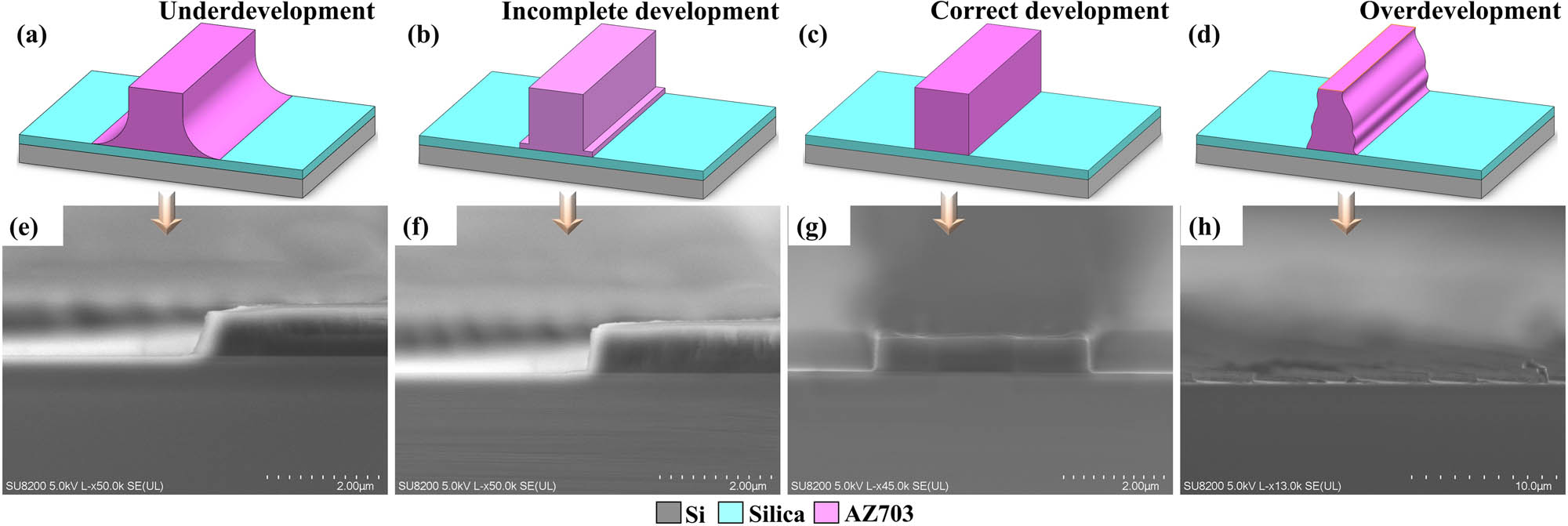
Photoresist development issues. (a) and (e) Schematic diagram and SEM image of photoresist underdevelopment, (b) and (f) schematic diagram and SEM image of incomplete photoresist development, (c) and (g) schematic diagram and SEM image of correct photoresist development, and (d) and (h) schematic diagram and SEM image of photoresist overdevelopment.
It can be seen that the development time directly affects the morphology of the photoresist pattern, thereby affecting the subsequent processing technology. Therefore, it is necessary to study the effect of development time on the morphology of the photoresist pattern. Figure 3 shows the microscopic images and scanning electron microscopy (SEM) image at different development times. When the development time is 30 s, the pattern lines of the photoresist are clear (Figure 3(a)), and the sidewalls of the photoresist are steep (Figure 3(b)), which is the optimal development time. When the development time is extended to 45 s, local corrosion occurs in the photoresist pattern, and a large number of corrosion points can be seen in the microscope image (Figure 3(c)). When the development time is 90 s, the photoresist pattern collapses and distorts. If the time is further extended, the photoresist pattern may even disappear.

Microscopic images of photoresists under different development times. (a) 30 s, (b) SEM image of photoresist with development time of 30 s, (c) 45 s, and (d) 90 s.
3.2 The influence of etching time on etching width
Etching time seriously affects the etching width and thus the nanochannel size. Therefore, it is necessary to study the effect of etching time on etching width. Figure 4 shows the cross-sectional profiles of the etched sample, the SEM (SU8220, Hitachi, Japan) images are shown on the left (Figure 4(a)), and the schematic diagram listing the dimensions of the etched sample is shown on the right (Figure 4(b)).

Schematic diagram of the wet etching process. (a) SEM image of the etched sample, (b) schematic diagram listing the dimensions of the etched sample (W is the etching width (t > 11 s), and H is the depth of nanochannel equal to the etching thickness of silica).
Because wet etching has the inherent property of etching any exposed surface, that is, isotropic etching. Therefore, during the initial stages of wet etching, the sidewalls are usually etched at a rate similar to the bottom, producing a lateral undercut distance of the same order as the etching depth, resulting in a curve profile whose radius is approximately equal to the etching depth, as shown in Figure 5(a), where the size of W 0 is approximately equal to H. When the etching time exceeds 11 s, the front of the etchant meets the stop layer (Si layer), the consumption of the etchant becomes less, the etching begins to accelerate in the horizontal direction, and the etching width gradually increases, and the SiO2 sidewalls gradually straighten, as shown in Figure 5(d).

The SEM images of the etched sample under different etching times. (a) etching time 11 s, (b) etching time 15 s, (c) etching time 17 s, and (d) etching time 22 s.
From the curve of the relationship between etching time and etching width (Figure 6), it can be seen that as the etching time increases, the etching width gradually increases. The etching width could be predicted from the etching time by the following formula:
where t is the etching time and W is the etching width. The average correlation of curve fitting can reach R 2 = 0.97, indicating good agreement between experimental data and fitting data.

Relationship between etching time and etching width.
3.3 The reproducibility of the wet etching process
To study the reproducibility of the wet etching process, the samples were placed in the BHF solution and three different samples were wet etched with silica in a 60°C water bath for 15 s (Figure 7). The etching width of the three samples was measured. Their dimensions were as follows: (a) etching width was 108 ± 3 nm, (b) etching width was 106 ± 3 nm, and (c) etching width was 110 ± 1 nm. The maximum width difference in etching width between chips is 4 nm, the average etching width is 114 nm, and the width variation is about 4%. It can be seen that the BHF wet etching process has good repeatability.

SEM images of etching width etched by BHF in different chips. The SEM images of (a)–(c) show the etching width from three samples. The etching time is 15 s: (a) 108 ± 3 nm, (b) 106 ± 3 nm, and (c) 110 ± 1 nm.
3.4 The influence of metal deposition methods on the formation of nanogap
Figure 8 shows the schematic and SEM images of nanogap obtained at different angles of thermal evaporation.

Schematic and SEM images of nanogap and nanochannel obtained under different metal deposition methods. (a) schematic diagram of magnetron sputtering deposition, (b) schematic diagram of thermal evaporation deposition, (c) SEM image of nanotube obtained by magnetron sputtering deposition, (d) SEM image and enlarged image of nanotubes obtained by thermal evaporation deposition, (e) SEM image of nanochannel obtained after lift-off using magnetron sputtering deposition method, and (f) SEM image of nanochannel obtained after lift-off using thermal evaporation deposition method.
Magnetron sputtering deposition has isotropic characteristics (Figure 8(a)) and has the advantages of good deposition quality, uniform film thickness, and good bonding strength between the film and the substrate. Using magnetron sputtering deposition, the metal film will be evenly deposited on the target substrate, such as the horizontal surface of the photoresist, the side wall of the photoresist, the silicon substrate, and the junction between the photoresist and the substrate (Figure 8(c)). Therefore, in the subsequent lift-off process, the metal film is easy to tear and is not easy to form nanochannels (Figure 8(e)).
Unlike magnetron sputtering deposition, thermal evaporation has anisotropic characteristics (Figure 8(b)) and has the advantages of a simple process, short deposition time, and good deposition directionality. During the thermal evaporation process, the metal film on the side wall of the photoresist is not connected to the metal film on the silicon substrate (Figure 8(d)). After the sample was lifted off, there was no connection between the metal film on the photoresist and the metal film on the substrate, indicating that thermal evaporation cannot form sealed nanotubes. After being lifted off, the metal film on the photoresist is not connected to the metal film on the substrate, so no tearing occurs, thus forming a nanochannel (Figure 8(f)). Therefore, thermal evaporation is more suitable for this process.
3.5 Fabrication of polymer nanochannel using the PDMS nano-mold
Figure 9 shows SEM images of nanochannels at different etching times. As the figure shows, the nanochannel size can be effectively controlled by changing the etching time. As the etching time increases, the nanochannel width gradually increases. When the etching time was 13 s, a nanochannel with a size of 82 nm in width and 56 nm in depth was obtained (Figure 9(a)). However, nanochannels based on silicon substrates are prone to brittle cracks if they are directly used as molds for hot embossing. Therefore, this article pours PDMS on the nanochannels to replicate the nanochannel pattern, thereby obtaining a convex PDMS nano-mold, in which the nano-ridge width is 82 ± 7 nm and the height is 40 ± 6 nm (Figure 10(a) and (b)). PDMS has good flatness and is easy to de-mold [37,38]. The SU-8 photoresist was imprinted with a convex PDMS nano-mold at 85°C for 20 min to transfer the nanopattern to the SU-8 substrate, and finally, a nanochannel with a width of 74 ± 9 nm and a depth of 37 ± 7 nm was obtained.

SEM images of nanochannel obtained under different etching times. (a) 82 nm wide and 56 nm deep nanochannel resulting from etching time of 13 s, (b) 108 nm wide and 55 nm deep nanochannel resulting from etching time of 15 s, (c) 167 nm wide and 86 nm deep nanochannel resulting from etching time of 20 s, and (d) 242 nm wide and 88 nm deep nanochannel resulting from etching time of 25 s.

SEM images of PDMS nano-mold and SU-8 nanochannel: (a) PDMS nano-mold with a width of 82 ± 7 nm and a height of 40 ± 6 nm, (b) SEM image of PDMS nano-mold, and (c) SU-8 nanochannel width 74 ± 9 nm, depth 37 ± 7 nm.
PDMS nano-molds with sizes less than 100 nm were successfully prepared by the deposition casting method proposed in this study. With this method, different sizes of nanochannels can be obtained by precisely controlling the wet etching parameters. In future studies, the duty cycle of the nanochannels can also be adjusted by changing the width of the photoresist mesas. However, there are still some limitations of this method that need to be overcome: (1) Since wet etching has the characteristic of isotropic etching, the preparation of molds by this method cannot produce molds with a width less than the depth. In future research, only the silica layer and the metal layer can be used as a mask, and then the dry etching process is used to etch the silicon substrate, and the silicon nano-molds with a higher depth-to-width ratio can be obtained by optimizing the parameters of the dry etching, but its production cost will also be greatly increased. Alternatively, metal deposition or parylene film deposition is performed on the mold after the lift-off process. Since the thickness of the metal and silica layer deposited on the surface by the deposition technique is much thicker compared to the thickness deposited on the sidewalls of the nanochannel and on the bottom of the nanochannel, the depth of the nanochannel increases rapidly, resulting in molds with widths that are less than the depth. (2) The nano-ridges on the PDMS nano-mold are not perfectly straight. A slight unevenness in the lines of the photolithography mask used in this study caused deformation, which led to a series of deformations in the silica layer, photoresist, and nanochannels. It is highly recommended that a photolithography mask with higher accuracy be used in future studies.
4 Conclusions
In this study, a sub-100 nm PDMS nano-mold was successfully fabricated by the side etching deposition casting method. We studied the effect of development time on the morphology of photoresists. A slope or a layer of stepped film at the bottom of the photoresist results from the development time being too short, which prevents the development solution from completely reacting with the photoresist. Overly extended development times can cause the photoresist to disintegrate or vanish. The influence of etching time on etching width was investigated. The impact of thermal evaporation and magnetron sputtering deposition methods on the formation of nanochannels was analyzed, and it was found that the anisotropic deposition characteristics of thermal evaporation better meet the needs of nanochannel preparation technology. Finally, PDMS nano-mold with a width of 82 ± 7 nm and a height of 40 ± 6 nm was prepared under optimized parameters.
Acknowledgments
The authors are grateful for the reviewers valuable comments that improved the manuscript.
-
Funding information: This research work was supported by the Excellent Postdoctoral Program of Jiangsu Province (No. 2023ZB694).
-
Author contributions: All authors have accepted responsibility for the entire content of this manuscript and approved its submission.
-
Conflict of interest: The authors state no conflict of interest.
-
Data availability statement: The datasets generated and/or analyzed during the current study are available from the corresponding author on reasonable request.
References
[1] Kasani S, Curtin K, Wu N. A review of 2D and 3D plasmonic nanostructure array patterns: fabrication, light management and sensing applications. Nanophotonics. 2019;8(12):2065–89.10.1515/nanoph-2019-0158Search in Google Scholar
[2] Zhao ZJ, Ahn J, Hwang SH, Ko J, Jeong Y, Bok M, et al. Large-area nanogap-controlled 3D nanoarchitectures fabricated via layer-by-layer nanoimprint. ACS Nano. 2021;15(1):503–14.10.1021/acsnano.0c05290Search in Google Scholar PubMed
[3] Jia Y, Chen F. Recent progress on femtosecond laser micro-/nano-fabrication of functional photonic structures in dielectric crystals: A brief review and perspective. APL Photonics. 2023;8(9):090901.10.1063/5.0160067Search in Google Scholar
[4] Zhang X, Liu H, Jiang L. Wettability and applications of nanochannels. Adv Mater. 2019;31(5):e1804508.10.1002/adma.201804508Search in Google Scholar PubMed
[5] Feng HQ, Shen ST, Jin ML, Zhang QL, Liu MJ, Wu ZH, et al. Microwell confined electro-coalescence for rapid formation of high-throughput droplet array. Small. 2023;19(45):2302998.10.1002/smll.202302998Search in Google Scholar PubMed
[6] Rahman M, Islam KR, Islam MR, Islam MJ, Kaysir MR, Akter M, et al. A critical review on the sensing, control, and manipulation of single molecules on optofluidic devices. Micromachines. 2022;13(6):968.10.3390/mi13060968Search in Google Scholar PubMed PubMed Central
[7] Higgins SG, Becce M, Belessiotis-Richards A, Seong H, Sero JE, Stevens MM. High-aspect-ratio nanostructured surfaces as biological metamaterials. Adv Mater. 2020;32(9):e1903862.10.1002/adma.201903862Search in Google Scholar PubMed PubMed Central
[8] Huang L, Yang DY, Yu ZM, He JX, Chen Y, Zhou JH. Deep learning-aided high-throughput screening of time-resolved protein crystallization on programmable microliter-droplet systems. Chem Eng J. 2022;450:138267.10.1016/j.cej.2022.138267Search in Google Scholar
[9] Alfaro JA, Bohländer P, Dai MJ, Filius M, Howard CJ, van Kooten XF, et al. The emerging landscape of single-molecule protein sequencing technologies. Nat Methods. 2021;18(6):604–17.10.1038/s41592-021-01143-1Search in Google Scholar PubMed PubMed Central
[10] Mahajan S, Sharkins JA, Hunter AH, Avishai A, Ereifej ES. Focused ion beam lithography to etch nano-architectures into microelectrodes. J Visualized Exp. 2020;155:e60004.10.3791/60004Search in Google Scholar PubMed PubMed Central
[11] Manoccio M, Esposito M, Passaseo A, Cuscuna M, Tasco V. Focused ion beam processing for 3D chiral photonics nanostructures. Micromachines. 2021;12(1):6.10.3390/mi12010006Search in Google Scholar PubMed PubMed Central
[12] He S, Tian R, Wu W, Li W-D, Wang D. Helium-ion-beam nanofabrication: extreme processes and applications. Int J Extreme Manuf. 2021;3(1):012001.10.1088/2631-7990/abc673Search in Google Scholar
[13] Li P, Chen S, Dai H, Yang Z, Chen Z, Wang Y, et al. Recent advances in focused ion beam nanofabrication for nanostructures and devices: fundamentals and applications. Nanoscale. 2021;13(3):1529–65.10.1039/D0NR07539FSearch in Google Scholar
[14] Tavares L, Chiriaev S, Adashkevich V, Taboryski R, Rubahn HG. Height patterning of nanostructured surfaces with a focused helium ion beam: a precise and gentle non-sputtering method. Nanotechnology. 2020;31(14):145303.10.1088/1361-6528/ab6679Search in Google Scholar PubMed
[15] Petrov YV, Grigoryev EA, Baraban AP. Helium focused ion beam irradiation with subsequent chemical etching for the fabrication of nanostructures. Nanotechnology. 2020;31(21):215301.10.1088/1361-6528/ab6fe3Search in Google Scholar PubMed
[16] Jee H, Park M-J, Jeon K, Jeong C, Lee J. Combining interference lithography and two-photon lithography for fabricating large-area photonic crystal structures with controlled defects. Appl Sciences-Basel. 2021;11(14):6559.10.3390/app11146559Search in Google Scholar
[17] Valsecchi C, Gomez Armas LE, de Menezes JW. Large area nanohole arrays for sensing fabricated by interference lithography. Sensors. 2019;19(9):2182.10.3390/s19092182Search in Google Scholar PubMed PubMed Central
[18] Hreshchuk OM, Yukhymchuk VO, Dzhagan VM, Danko VA, Minko VI, Indutnyi IZ, et al. Efficient SERS substrates based on laterally ordered gold nanostructures made using interference lithography. Semicond Phys Quantum Electron Optoelectron. 2019;22(2):215–23.10.15407/spqeo22.02.215Search in Google Scholar
[19] Holmes J, Zhang M, Greibe T, Schaich WL, Jacobson SC, Dragnea B. Mapping complex profiles of light intensity with interferometric lithography. Nanoscale Adv. 2023;5(7):2045–53.10.1039/D2NA00570KSearch in Google Scholar PubMed PubMed Central
[20] Sasidharan V, Neumann A, Brueck SRJ. Diffraction-grating beam splitter, interferometric-lithography nanopatterning with a multilongitudinal-mode diode laser. J Vac Sci Technol B. 2021;39(6):062603.10.1116/6.0001377Search in Google Scholar
[21] Chen M, Wang Z, Ge X, Wang Z, Fujisawa K, Xia J, et al. Controlled fragmentation of single-atom-thick polycrystalline graphene. Matter . 2019;2(3):666–79.10.1016/j.matt.2019.11.004Search in Google Scholar
[22] Zhang C, Wu M, Li M, Che L, Tan Z, Guo D, et al. A nanonewton-scale biomimetic mechanosensor. Microsyst Nanoeng. 2023;9:87.10.1038/s41378-023-00560-wSearch in Google Scholar PubMed PubMed Central
[23] Zhang C, Wu M, Cao S, Liu M, Guo D, Kang Z, et al. Bioinspired environment-adaptable and ultrasensitive multifunctional electronic skin for human healthcare and robotic sensations. Small. 2023;19(41):e2304004.10.1002/smll.202304004Search in Google Scholar PubMed
[24] Namdari N, Mohammadian B, Jafari P, Mohammadi R, Sojoudi H, Ghasemi H, et al. Advanced functional surfaces through controlled damage and instabilities. Mater Horiz. 2020;7(2):366–96.10.1039/C9MH01516GSearch in Google Scholar
[25] Zhou Y, Zhan P, Ren M, Zheng G, Dai K, Mi L, et al. Significant stretchability enhancement of a crack-based strain sensor combined with high sensitivity and superior durability for motion monitoring. ACS Appl Mater Interfaces. 2019;11(7):7405–14.10.1021/acsami.8b20768Search in Google Scholar PubMed
[26] Zhang S, Liu H, Yang S, Shi X, Zhang D, Shan C, et al. Ultrasensitive and highly compressible piezoresistive sensor based on polyurethane sponge coated with a cracked cellulose nanofibril/silver nanowire layer. ACS Appl Mater Interfaces. 2019;11(11):10922–32.10.1021/acsami.9b00900Search in Google Scholar PubMed
[27] Chou SY. Sub-10 nm imprint lithography and applications. J Vac Sci Technol B: Microelectron Nanometer Struct. 1997;15(6):032002.10.1116/1.589752Search in Google Scholar
[28] Zhang L, Yan JW. Study on nano-graphitic carbon coating on Si mold insert for precision glass molding. Surf Coat Technol. 2022;448:128893.10.1016/j.surfcoat.2022.128893Search in Google Scholar
[29] Moon J, Kwon S, Alahbakhshi M, Lee Y, Cho K, Zakhidov A, et al. Surface energy-driven preferential grain growth of metal halide perovskites: effects of nanoimprint lithography beyond direct patterning. ACS Appl Mater Interfaces. 2021;13(4):5368–78.10.1021/acsami.0c17655Search in Google Scholar PubMed
[30] Cates N, Einck V, Micklow L, Morere J, Okoroanyanwu U, Watkins JJ, et al. Roll-to-roll nanoimprint lithography using a seamless cylindrical mold nanopatterned with a high-speed mastering process. Nanotechnology. 2021;32(15):155301.10.1088/1361-6528/abd9f1Search in Google Scholar PubMed
[31] Mizoshita N, Yamada Y, Murase M, Goto Y, Inagaki S. Direct nanoimprinting of nanoporous organosilica films consisting of covalently crosslinked photofunctional frameworks. Nanoscale. 2020;12(41):21146–54.10.1039/D0NR03272GSearch in Google Scholar PubMed
[32] Guo R, Yan G, Niu W, Li X. Fabrication of SU-8 polymer micro/nanoscale nozzle by hot embossing method. Nanotechnology. 2024;35(25):255301.10.1088/1361-6528/ad3252Search in Google Scholar PubMed
[33] Guo R, Li X, Niu W, Feng J. Oxygen plasma assisted room temperature bonding for manufacturing SU-8 polymer micro/nanoscale nozzle. Nanotechnol Rev. 2023;12(1):20230113.10.1515/ntrev-2023-0113Search in Google Scholar
[34] Rao J, Zou H, Syms RRA, Cheng E, Liu C. Fabrication of 2D silicon nano-mold based on sidewall transfer. Micro Nano Lett. 2011;6(1):29–33.10.1049/mnl.2010.0155Search in Google Scholar
[35] Yin Z, Qi L, Zou H, Sun L. A novel 2D silicon nano-mold fabrication technique for linear nanochannels over a 4 inch diameter substrate. Sci Rep. 2016;6:18921.10.1038/srep18921Search in Google Scholar PubMed PubMed Central
[36] Sun L, Zou H, Sang S. A low-cost and high-efficiency method for four-inch silicon nano-mold by proximity UV exposure. Nanotechnology. 2021;33(7):075303.10.1088/1361-6528/ac25abSearch in Google Scholar PubMed
[37] Zhu X, Li Y, Shi Y, Hou L, Wang G, He Z, et al. Structure–mechanical property relationships of 3D-printed porous polydimethylsiloxane films. Nanotechnol Rev. 2023;12(1):20230188.10.1515/ntrev-2023-0188Search in Google Scholar
[38] He Z, Su J, Zhu X, Li Y, Yang L, Zhang X, et al. Integrated structure-function design of 3D-printed porous polydimethylsiloxane for superhydrophobic engineering. Rev Adv Mater Sci. 2024;63(1):20240074.10.1515/rams-2024-0074Search in Google Scholar
© 2025 the author(s), published by De Gruyter
This work is licensed under the Creative Commons Attribution 4.0 International License.
Articles in the same Issue
- Research Articles
- MHD radiative mixed convective flow of a sodium alginate-based hybrid nanofluid over a convectively heated extending sheet with Joule heating
- Experimental study of mortar incorporating nano-magnetite on engineering performance and radiation shielding
- Multicriteria-based optimization and multi-variable non-linear regression analysis of concrete containing blends of nano date palm ash and eggshell powder as cementitious materials
- A promising Ag2S/poly-2-amino-1-mercaptobenzene open-top spherical core–shell nanocomposite for optoelectronic devices: A one-pot technique
- Biogenic synthesized selenium nanoparticles combined chitosan nanoparticles controlled lung cancer growth via ROS generation and mitochondrial damage pathway
- Fabrication of PDMS nano-mold by deposition casting method
- Stimulus-responsive gradient hydrogel micro-actuators fabricated by two-photon polymerization-based 4D printing
- Physical aspects of radiative Carreau nanofluid flow with motile microorganisms movement under yield stress via oblique penetrable wedge
- Effect of polar functional groups on the hydrophobicity of carbon nanotubes-bacterial cellulose nanocomposite
- Review in green synthesis mechanisms, application, and future prospects for Garcinia mangostana L. (mangosteen)-derived nanoparticles
- Entropy generation and heat transfer in nonlinear Buoyancy–driven Darcy–Forchheimer hybrid nanofluids with activation energy
- Green synthesis of silver nanoparticles using Ginkgo biloba seed extract: Evaluation of antioxidant, anticancer, antifungal, and antibacterial activities
- A numerical analysis of heat and mass transfer in water-based hybrid nanofluid flow containing copper and alumina nanoparticles over an extending sheet
- Investigating the behaviour of electro-magneto-hydrodynamic Carreau nanofluid flow with slip effects over a stretching cylinder
- Electrospun thermoplastic polyurethane/nano-Ag-coated clear aligners for the inhibition of Streptococcus mutans and oral biofilm
- Investigation of the optoelectronic properties of a novel polypyrrole-multi-well carbon nanotubes/titanium oxide/aluminum oxide/p-silicon heterojunction
- Novel photothermal magnetic Janus membranes suitable for solar water desalination
- Green synthesis of silver nanoparticles using Ageratum conyzoides for activated carbon compositing to prepare antimicrobial cotton fabric
- Activation energy and Coriolis force impact on three-dimensional dusty nanofluid flow containing gyrotactic microorganisms: Machine learning and numerical approach
- Machine learning analysis of thermo-bioconvection in a micropolar hybrid nanofluid-filled square cavity with oxytactic microorganisms
- Research and improvement of mechanical properties of cement nanocomposites for well cementing
- Thermal and stability analysis of silver–water nanofluid flow over unsteady stretching sheet under the influence of heat generation/absorption at the boundary
- Cobalt iron oxide-infused silicone nanocomposites: Magnetoactive materials for remote actuation and sensing
- Magnesium-reinforced PMMA composite scaffolds: Synthesis, characterization, and 3D printing via stereolithography
- Bayesian inference-based physics-informed neural network for performance study of hybrid nanofluids
- Numerical simulation of non-Newtonian hybrid nanofluid flow subject to a heterogeneous/homogeneous chemical reaction over a Riga surface
- Enhancing the superhydrophobicity, UV-resistance, and antifungal properties of natural wood surfaces via in situ formation of ZnO, TiO2, and SiO2 particles
- Synthesis and electrochemical characterization of iron oxide/poly(2-methylaniline) nanohybrids for supercapacitor application
- Impacts of double stratification on thermally radiative third-grade nanofluid flow on elongating cylinder with homogeneous/heterogeneous reactions by implementing machine learning approach
- Synthesis of Cu4O3 nanoparticles using pumpkin seed extract: Optimization, antimicrobial, and cytotoxicity studies
- Cationic charge influence on the magnetic response of the Fe3O4–[Me2+ 1−y Me3+ y (OH2)] y+(Co3 2−) y/2·mH2O hydrotalcite system
- Pressure sensing intelligent martial arts short soldier combat protection system based on conjugated polymer nanocomposite materials
- Magnetohydrodynamics heat transfer rate under inclined buoyancy force for nano and dusty fluids: Response surface optimization for the thermal transport
- Fly ash and nano-graphene enhanced stabilization of engine oil-contaminated soils
- Enhancing natural fiber-reinforced biopolymer composites with graphene nanoplatelets: Mechanical, morphological, and thermal properties
- Performance evaluation of dual-scale strengthened co-bonded single-lap joints using carbon nanotubes and Z-pins with ANN
- Computational works of blood flow with dust particles and partially ionized containing tiny particles on a moving wedge: Applications of nanotechnology
- Hybridization of biocomposites with oil palm cellulose nanofibrils/graphene nanoplatelets reinforcement in green epoxy: A study of physical, thermal, mechanical, and morphological properties
- Design and preparation of micro-nano dual-scale particle-reinforced Cu–Al–V alloy: Research on the aluminothermic reduction process
- Spectral quasi-linearization and response optimization on magnetohydrodynamic flow via stenosed artery with hybrid and ternary solid nanoparticles: Support vector machine learning
- Ferrite/curcumin hybrid nanocomposite formulation: Physicochemical characterization, anticancer activity, and apoptotic and cell cycle analyses in skin cancer cells
- Enhanced therapeutic efficacy of Tamoxifen against breast cancer using extra virgin olive oil-based nanoemulsion delivery system
- A titanium oxide- and silver-based hybrid nanofluid flow between two Riga walls that converge and diverge through a machine-learning approach
- Enhancing convective heat transfer mechanisms through the rheological analysis of Casson nanofluid flow towards a stagnation point over an electro-magnetized surface
- Intrinsic self-sensing cementitious composites with hybrid nanofillers exhibiting excellent piezoresistivity
- Research on mechanical properties and sulfate erosion resistance of nano-reinforced coal gangue based geopolymer concrete
- Impact of surface and configurational features of chemically synthesized chains of Ni nanostars on the magnetization reversal process
- Porous sponge-like AsOI/poly(2-aminobenzene-1-thiol) nanocomposite photocathode for hydrogen production from artificial and natural seawater
- Multifaceted insights into WO3 nanoparticle-coupled antibiotics to modulate resistance in enteric pathogens of Houbara bustard birds
- Synthesis of sericin-coated silver nanoparticles and their applications for the anti-bacterial finishing of cotton fabric
- Enhancing chloride resistance of freeze–thaw affected concrete through innovative nanomaterial–polymer hybrid cementitious coating
- Development and performance evaluation of green aluminium metal matrix composites reinforced with graphene nanopowder and marble dust
- Morphological, physical, thermal, and mechanical properties of carbon nanotubes reinforced arrowroot starch composites
- Influence of the graphene oxide nanosheet on tensile behavior and failure characteristics of the cement composites after high-temperature treatment
- Central composite design modeling in optimizing heat transfer rate in the dissipative and reactive dynamics of viscoplastic nanomaterials deploying Joule and heat generation aspects
- Double diffusion of nano-enhanced phase change materials in connected porous channels: A hybrid ISPH-XGBoost approach
- Synergistic impacts of Thompson–Troian slip, Stefan blowing, and nonuniform heat generation on Casson nanofluid dynamics through a porous medium
- Optimization of abrasive water jet machining parameters for basalt fiber/SiO2 nanofiller reinforced composites
- Enhancing aesthetic durability of Zisha teapots via TiO2 nanoparticle surface modification: A study on self-cleaning, antimicrobial, and mechanical properties
- Nanocellulose solution based on iron(iii) sodium tartrate complexes
- Combating multidrug-resistant infections: Gold nanoparticles–chitosan–papain-integrated dual-action nanoplatform for enhanced antibacterial activity
- Novel royal jelly-mediated green synthesis of selenium nanoparticles and their multifunctional biological activities
- Direct bandgap transition for emission in GeSn nanowires
- Synthesis of ZnO nanoparticles with different morphologies using a microwave-based method and their antimicrobial activity
- Numerical investigation of convective heat and mass transfer in a trapezoidal cavity filled with ternary hybrid nanofluid and a central obstacle
- Halloysite nanotube enhanced polyurethane nanocomposites for advanced electroinsulating applications
- Low molar mass ionic liquid’s modified carbon nanotubes and its role in PVDF crystalline stress generation
- Green synthesis of polydopamine-functionalized silver nanoparticles conjugated with Ceftazidime: in silico and experimental approach for combating antibiotic-resistant bacteria and reducing toxicity
- Evaluating the influence of graphene nano powder inclusion on mechanical, vibrational and water absorption behaviour of ramie/abaca hybrid composites
- Dynamic-behavior of Casson-type hybrid nanofluids due to a stretching sheet under the coupled impacts of boundary slip and reaction-diffusion processes
- Influence of polyvinyl alcohol on the physicochemical and self-sensing properties of nano carbon black reinforced cement mortar
- Advanced machine learning approaches for predicting compressive and flexural strength of carbon nanotube–reinforced cement composites: a comparative study and model interpretability analysis
- Review Articles
- A comprehensive review on hybrid plasmonic waveguides: Structures, applications, challenges, and future perspectives
- Nanoparticles in low-temperature preservation of biological systems of animal origin
- Fluorescent sulfur quantum dots for environmental monitoring
- Nanoscience systematic review methodology standardization
- Nanotechnology revolutionizing osteosarcoma treatment: Advances in targeted kinase inhibitors
- AFM: An important enabling technology for 2D materials and devices
- Carbon and 2D nanomaterial smart hydrogels for therapeutic applications
- Principles, applications and future prospects in photodegradation systems
- Do gold nanoparticles consistently benefit crop plants under both non-stressed and abiotic stress conditions?
- An updated overview of nanoparticle-induced cardiovascular toxicity
- Arginine as a promising amino acid for functionalized nanosystems: Innovations, challenges, and future directions
- Advancements in the use of cancer nanovaccines: Comprehensive insights with focus on lung and colon cancer
- Membrane-based biomimetic delivery systems for glioblastoma multiforme therapy
- The drug delivery systems based on nanoparticles for spinal cord injury repair
- Green synthesis, biomedical effects, and future trends of Ag/ZnO bimetallic nanoparticles: An update
- Application of magnesium and its compounds in biomaterials for nerve injury repair
- Micro/nanomotors in biomedicine: Construction and applications
- Hydrothermal synthesis of biomass-derived CQDs: Advances and applications
- Research progress in 3D bioprinting of skin: Challenges and opportunities
- Review on bio-selenium nanoparticles: Synthesis, protocols, and applications in biomedical processes
- Gold nanocrystals and nanorods functionalized with protein and polymeric ligands for environmental, energy storage, and diagnostic applications: A review
- An in-depth analysis of rotational and non-rotational piezoelectric energy harvesting beams: A comprehensive review
- Advancements in perovskite/CIGS tandem solar cells: Material synergies, device configurations, and economic viability for sustainable energy
- Deep learning in-depth analysis of crystal graph convolutional neural networks: A new era in materials discovery and its applications
- Review of recent nano TiO2 film coating methods, assessment techniques, and key problems for scaleup
- Antioxidant quantum dots for spinal cord injuries: A review on advancing neuroprotection and regeneration in neurological disorders
- Rise of polycatecholamine ultrathin films: From synthesis to smart applications
- Advancing microencapsulation strategies for bioactive compounds: Enhancing stability, bioavailability, and controlled release in food applications
- Advances in the design and manipulation of self-assembling peptide and protein nanostructures for biomedical applications
- Photocatalytic pervious concrete systems: from classic photocatalysis to luminescent photocatalysis
- Corrigendum
- Corrigendum to “Synthesis and characterization of smart stimuli-responsive herbal drug-encapsulated nanoniosome particles for efficient treatment of breast cancer”
- Special Issue on Advanced Nanomaterials for Carbon Capture, Environment and Utilization for Energy Sustainability - Part III
- Efficiency optimization of quantum dot photovoltaic cell by solar thermophotovoltaic system
- Exploring the diverse nanomaterials employed in dental prosthesis and implant techniques: An overview
- Electrochemical investigation of bismuth-doped anode materials for low‑temperature solid oxide fuel cells with boosted voltage using a DC-DC voltage converter
- Synthesis of HfSe2 and CuHfSe2 crystalline materials using the chemical vapor transport method and their applications in supercapacitor energy storage devices
- Special Issue on Green Nanotechnology and Nano-materials for Environment Sustainability
- Influence of nano-silica and nano-ferrite particles on mechanical and durability of sustainable concrete: A review
- Surfaces and interfaces analysis on different carboxymethylation reaction time of anionic cellulose nanoparticles derived from oil palm biomass
- Processing and effective utilization of lignocellulosic biomass: Nanocellulose, nanolignin, and nanoxylan for wastewater treatment
- Retraction
- Retraction of “Aging assessment of silicone rubber materials under corona discharge accompanied by humidity and UV radiation”