Analysis of Microstrip Line Fed Patch Antenna for Wireless Communications
-
Ashish Singh
Ashish Singh received his B.Tech degree in Applied Electronics and Instrumentation from the Uttar Pradesh Technical University, India, in 2007. He completed his M.Tech. and D.Phil. degrees in Communication Technology from Department of Electronics and Communication, University of Allahabad in 2009 and 2015 respectively. He has published more than 40 research papers in different national and international journals and conference proceedings. His are of interests are Patch Antenna, Millimeter waves, Optical communication and Bio-medical Instrumentation. He worked as an Assistant Professor in Raghu Engineering College, Visakhapatnam. Presently, he is working at same designation in NMAMIT, Nitte India. ,
Mohammad Aneesh
,
Mohammad Aneesh
Mohamad Aneesh received his B.Tech. Degree in Electrical and Electronics Engineering from Uttar Pradesh Technical University, India in 2007 and completed his M. Tech degree in Advance Communications System form Sam Higginbottom Institute of Agriculture, Technology & Sciences Allahabad, India in 2009 and completed his D.Phil. degree from Dept. of Electronics & Communication University of Allahabad, Allahabad, India in 2015. He has published more than 40 research papers in different national and international journals and conference proceedings. His areas of interest are Patch antenna, Neural Network, and Optical communication. He worked as Assistant Professor in Dr. Rizivi College of Engineering, Kaushambi. Nowadays. he is working as Assistant Professor in Dr. Ambedkar Institute of Technology for Handicapped, Kanpur, India-208024.Kamakshi received her B.Tech. degree in Electronics Engineering from the Institute of Engineering and Rural Technology Allahabad, U.P., India in 2007. She completed her M.Tech. and D.Phil. degrees in Communication Technology from Department of Electronics and Communication, University of Allahabad in 2009 and 2017 respectively. She has published more than 40 research papers in different national and international journals and conference proceedings. Her area of interests is Broadband antennas, and Millimeter waves. Nowadays, she is working as an Assistant Professor in IMS Engineering College, Ghaziabad, India.J. A. Ansari was born in 1966 in Gahmar, Ghazipur (U.P.), India. He received the B.Sc. and B.Tech. degrees in Electronics and Telecommunications from University of Allahabad, Allahabad, India. The M.Tech. degree in Communication Systems from the Institute of Technology, Banaras Hindu University (BHU), Varanasi, India, in 1991 and the Ph.D. degree from Mahatma Gandhi Chitrakoot Gramodaya Vishvavidyalaya, Chitrakoot (Satna), India, in 2000. He has published 100 research papers in different national and international journals and conference proceedings. His current area of research is microstrip antenna, millimeter wave, and fiber optics. He is presently working as a Professor with the Department of Electronics and Communication, University of Allahabad, Allahabad, India.

Abstract
In this paper, theoretical analysis of microstrip line fed rectangular patch antenna loaded with parasitic element and split-ring resonator is presented. The proposed antenna shows that the dualband operation depends on gap between parasitic element, split-ring resonator, length and width of microstrip line. It is found that antenna resonates at two distinct resonating modes i.e., 0.9 GHz and 1.8 GHz for lower and upper resonance frequencies respectively. The antenna shows dual frequency nature with frequency ratio 2.0. The characteristics of microstrip line fed rectangular patch antenna loaded with parasitic element and split-ring resonator antenna is compared with other prototype microstrip line fed antennas. Further, the theoretical results are compared with simulated and reported experimental results, they are in close agreement.
1 Introduction
Nowadays, microstrip patch antennas are important device in wireless communication systems. These antennas have been successfully utilized in many communication systems [1,2,3] such as satellite communication/links (vehicular GPS), cellular communication system (GSM/CDMA), wireless personal area (Bluetooth links), wireless local area network (Wi-Fi) and synthetic aperture radar (SAR). There are different techniques by which these antennas can be designed for various wireless applications such as proximity coupling [4], aperture coupling [5,6], loading of notches [7], slots [8,9,10], parasitic elements [11], L-strip fed [12,13], microstrip line feeding [14,15,16,17,18,19]. One of the important techniques is inset feeding by which patch antenna can be excited to achieve dual-band and multi-band frequencies for wireless communications.
The various contributions of researchers and scientists on microstrip line feeding are reported such as, analysis and design of annular patch antenna with electromagnetically coupled microstrip feed line [14], crescent-shaped multiband planar monopole antenna for mobile wireless applications [15], microstrip antenna array formed by microstrip line fed tooth-like-slot patches [16], printed wide-slot antenna with a modified L-shaped microstrip line for wideband applications [17], microstrip line-fed printed wide-slot antenna with a parasitic center patch [18], broadband T-shaped microstrip-fed U-slot coupled patch antenna [19]. All the above reported papers are of microstrip line fed patch antennas which lack theoretical analysis, equivalent circuit diagram and has complicated antenna geometry.
In this view, the main objective of this paper is to present theoretical analysis, equivalent circuit diagram, total input impedance and radiating structures of microstrip line fed rectangular patch antenna with split-ring resonator (SRR)for wireless communications. Theoretical analysis of microstrip line fed rectangular patch antenna loaded with parasitic element and split-ring resonator has been presented using circuit theory concept based on modal expansion cavity model. The proposed antenna structures have been realized with the proto-type radiating structures to obtain dualband characteristics. Variation of dimensions of the proposed antenna for the gap between parasitic element, split-ring resonator, length and width of microstrip line are discussed in next section.
2 Antenna designs
A rectangular patch with SRR and parasitic patch antenna along with similar proto-type microstrip line fed patch antennas are shown in Fig. 1. The Fig. 1(a) shows the side view of antennas. Antenna 1 is shown in Fig. 1(b), conventional microsrtip line fed patch antenna of dimensions L×W is excited by the 50 Ω microstrip line. Antenna 2 is shown in Fig. 1(c), it is similar to the Antenna1 except it has parasitic element of dimension L×W and gap between the fed patch and parasitic patch is G. Figure 1(d)-(e) is the proposed radiating structure with top and bottom view. The proposed radiating structure is Antenna 3 which has SRR on ground plane and parasitic patch is placed parallel to the fed patch on same plane at a distance G. A rectangular patch of dimension L×W is fed through microstrip line fed. The feeding is given at end of microstrip line via coaxial connector of diameter 0.72 mm. Design specification of the antennas are given in Table 1.
(a)Side view microstrip line fed patch antennas(b) Simple microstrip line fed patch (antenna 1), (c) microstrip line fed patch with parasitic element (antenna 2),(d) Top View and (e) Bottom View of proposed microstrip line fed patch antenna (antenna 3).
Design specifications of microstrip line feed patch antennasare given as
| Thickness of dielectric substrate (H) | 1.5 mm |
|---|---|
| Permittivity of Substrate (εr) | 2.65 |
| Loss tangent of substrate (tanδ) | 0.0015 |
| Width of patch and parasitic patch (W) | 23 mm |
| Length of patch and parasitic patch (L) | 58 mm |
| Width of microstrip line (Ws) | 4.0 mm |
| Gap between the feed patch and parasitic patch (G) | 4.0 mm |
| Length of SRR’s (SL) | 25.6 mm |
| Width of SRR’s (Sw) | 25.6 mm |
| Width of both SRR’s arm (Sa) | 12.65 mm |
| Length of SRR’s arm (St) | 0.5 mm |
| Gap between two SRR’s arms (g1) | 0.5 mm |
| Length of Microstrip line (Ls) | 22.5 mm |
Figure 2 shows the current distribution on radiating structure of the Antenna 3 at lower (0.9 GHz) and upper (1.8 GHz) resonance frequencies. From the figure, it has been observed that proposed radiating structure has two directions of currents flowing on the radiating patch. The first is normal to the patch and other current flows due to the coupling between the fed patch with parasitic patch and the radiating patch with SRR. These combine mechanism provide dual band operation.
Current distribution (a) Lower and (b) higher resonance frequency.
3 Theortical analysis and its equivalent circuits
A simple rectangular patch is considered as a parallel combination of resistance R1, inductance L1, and capacitance C1 circuit and its input impedance is represented as Zp. The equivalent circuit of the rectangular patch is shown in Fig. 3(a), where R1, C1 and L1 can be defined as [20,21],
Quality factor,
Where
L- Length of rectangular patch,
W- Width of rectangular patch,
H- Thickness of the substrate material,
X0-x coordinates of feed point, i.e.,X0 = Ls,
εe - effective permittivity of the medium.
Equivalent Circuits diagram of (a) Simple patch (Zp) (b) parasitic patch (Zpp )(c) Gap between two patch (Zcc) (d) Microstrip line patch (ZL)
The equivalent circuit of the parasitic patch is shown in Fig. 3(b), its input impedance is represented as Zpp, where R2, C2 and L2can be calculated as R1, C1 and L1 with same equations, here X0 is considered as 0. The equivalent circuit diagram of the gap between the fed patch and the parasitic patch Zcc is shown in Fig. 3(c), which is represented as the combination of capacitances Cg and Cp1. The expression of gap capacitance Cg and plate capacitance Cp1 of the microstrip line can be calculated as [22,23,24]
Where,
CL is the terminal capacitance of the open circuited conductor is given as,
where Cll is the conductor extension length, εeff is effective dielectric constant.
Z0is characteristic impedance of the patch, c is the velocity of light.
The microstrip line of the rectangular patch is considered as combination of L and C. The equivalent circuit of the microstrip line rectangular patch is shown in Fig. 3(d), where LL and CL are inductance and capacitance of strip [22, 23].
Resonance frequency of the microstrip line antenna is given as,
where
Les = LS +ΔLS,
εre- Effective dielectric constant,
Les -Effective increase in length of strip,
εr -Dielectric constant,
The characteristic impedance of microstrip line [20,21,22],
Therefore, the total input impedance (Zin) of antenna can be calculated by equivalent circuit diagram Fig. 4 as
where Lc and Ccis the inductance and capacitance of SRR’s can calculated as [24].
Equivalent circuit diagram of the antenna.
Now using equation (10) the total input impedance of the proposed antenna is calculated. Their various antenna parameters such as reflection coefficient, VSWR and return loss are calculated as:
Reflection Coefficient
where
Z is the input impedance of the microstrip fed (50 Ω).
and RL=20 log |r|
4 Discussion of results
The antennas 1, 2, and 3 have been simulated using software IE3D based on Method of Moments. Figure 5 presents the variations of reflection coefficients for different radiating structures. Antenna1 is resonating at 4.1 GHz below −10 dB offer a bandwidth of 139 MHz (3.94-4.12 GHz) which can be utilized for satellite communication. Antenna 2 is resonating at three distinct frequency modes 3.144 GHz, 3.252 GHz and 3.804 GHz. In theses frequency bands only 3.804 GHz frequency has efficient bandwidth of 441 MHz (3.696-3.864 GHz) that can be utilized for down link in satellite communication. Antenna 3 resonates at two distinct frequencies modes 0.9 GHz and 1.8 GHz below −10 dB and meets the requirement of mobile communication. It is observed that on incorporating parasitic elements and SRR resonating frequencies shift toward lower side. This is due to the increase radiation resistance of the proposed antenna. There is a dip at 1.5 GHz in proposed antenna, this is observed because gap between the parasitic patch and fed as well as gap between SRR arms.
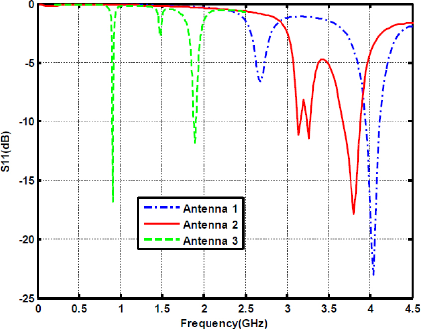
Comparisons of proposed antenna 3 with antennas 1 and 2.
Figure 6 shows the variation of reflection coefficient with frequency for the proposed antenna. The simulated, theoretical and reported experimental results of the microstrip line fed rectangular patch antenna with parasitic element and SRR are in close agreement. From figure it is observed that the antenna shows dual frequency behavior with frequency ratio 2.0 (Simulated) and 2.12 (theoretical). Theoretical results are based on circuit theory concept based on cavity model whereas simulated results are obtained using IE3D software that is based on Method of Moments. Further, analysis of the antenna 3 is shown in figures 7 to 10 which are based on circuit theory concept are described below.
![Figure 6 Comparison between theoretical, experimental [25] and simulated [26] results.](/document/doi/10.1515/eng-2017-0034/asset/graphic/j_eng-2017-0034_fig_006.jpg)
From Figure 7, it is observed that on decreasing the substrate thickness (H=1.5 mm to 0.5 mm) frequency ratio decreases from 2.0 to 1.27 whereas on increasing the substrate thickness (H=1.5 mm to 2.5 mm) frequency ratio increases to 2.96. This happens because on increasing and decreasing the height of the substrate equations (1), (4) and (6) are effected which is responsible for variation in resonance frequency of the radiating patch.
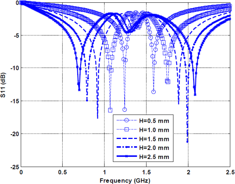
Variation of reflection coeflcient (dB) with frequency on varying height of the substrate(H).
Figure 8 shows the variation of reflection coefficient with frequency on decreasing (Ws=4 mm to 2 mm) and increasing (Ws =4 mm to 6 mm) the width of microstrip line, there is no change in the frequency ratio of upper to lower resonance frequency whereas slight shifting is observed on both upper and lower resonance frequencies. This is due to the capacitance CL which is directly proportion to width of microstrip line Ws, from equation (7).
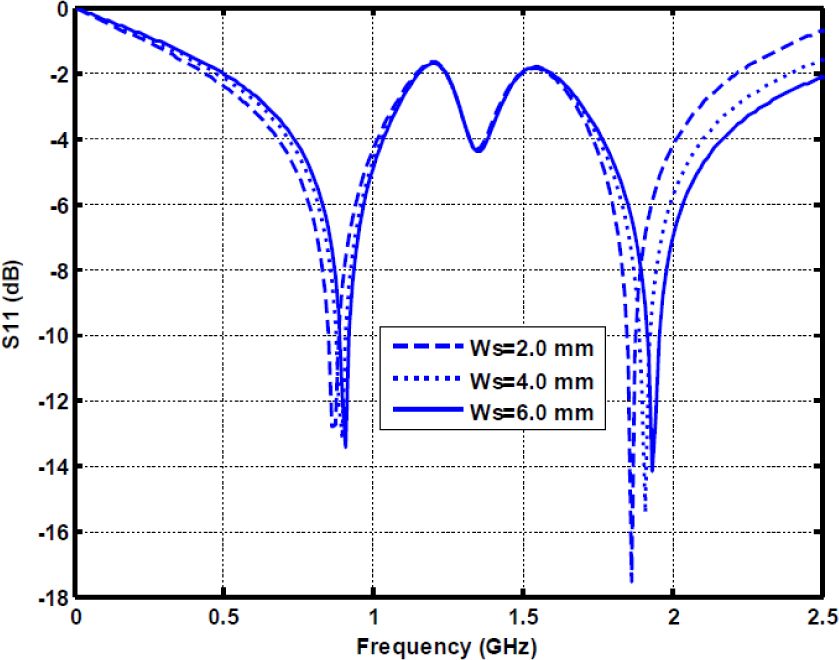
Variation of reflection coefficient (dB) with frequency on varying width of microstrip (Ws).
From Figure 9, it is observed that on increasing the length of the microstrip line (Ls =21.6 mm to 29.6 mm), lower and higher resonance frequencies shift towards lower resonance side whereas there is no change in the frequency ratio of upper to lower resonance frequency. This affects the equation (8) as resonance frequency of the microstrip line f is inversely proportional to the length microstrip line Ls.
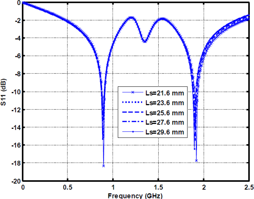
Variation of reflection coefficient (dB) with frequency on varying length of microstrip (Ls).
Figure 10 shows that on decreasing gap between the fed patch and parasitic patch (G=4 mm to 3 mm), the upper and lower resonance frequencies shift towards the lower side. Further, on increasing G=4 mm to 7 mm, upper and lower resonance frequencies shift towards higher side. This happens because the gap capacitance Cg is affected on increasing and decreasing the gap between fed patch and parasitic patch G i.e., from equation (4), Cg changes exponentially on variation of G. Thus, there is no huge variation on varying G.
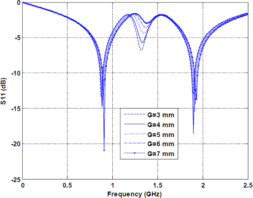
Variation of reflection coeflcient (dB) with frequency on varying gap between fed patch and parasitic patch.
From Figure 11, shows the radiation pattern at lower (0.9 GHz) and higher (1.8 GHz) resonance frequency and antenna shows circular polarization. The 3 dB beam width at lower resonance frequency for Etheta, phi=0° is 130.33° and Etheta, phi=90° is 88.92° whereas at higher resonance frequency for Etheta, phi=0 is 165.83° and Etheta, phi=0 is 83.7°.
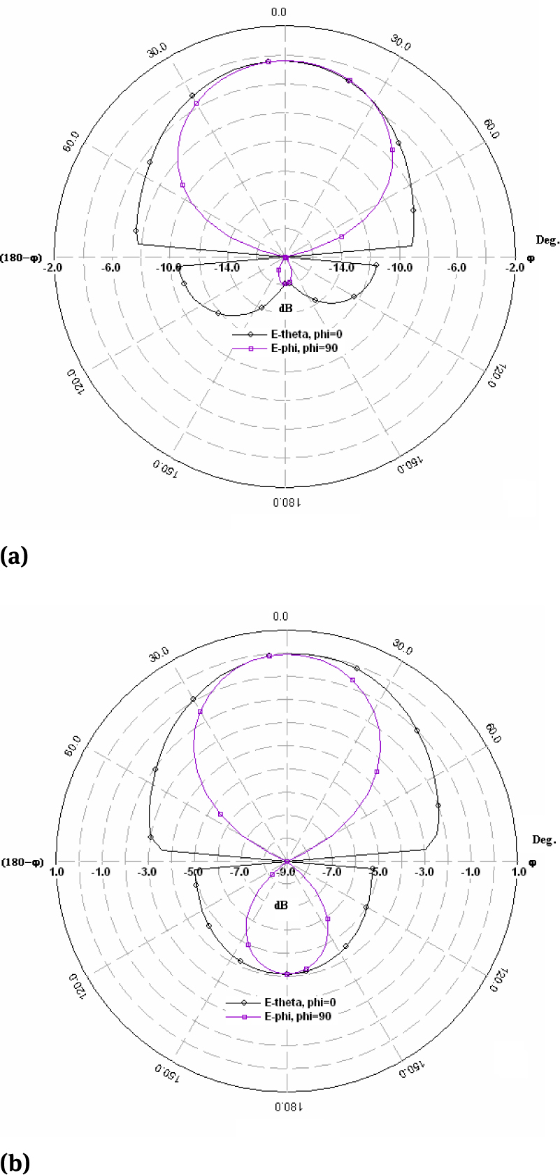
Radiation Pattern of antenna (a) Lower resonance frequency (b) Upper resonance frequency (Etheta, for phi=0 and phi=90 deg).
5 Conclusion
From the above analysis it is inferred that theoretical results are in close agreement with simulated and reported experimental results for inset fed rectangular patch antenna loaded with parasitic element and split ring resonator. The frequency ratio of the proposed antenna depends on microstrip length and width, thickness of dielectric substrate and gap between parasitic patch. The proposed antenna has frequency ratio 2.0 and maximum gain 1.8 dBi. The proposed antennas can be utilized for wireless communications such as mobiles and down linking for satellite communications.
About the authors

Ashish Singh received his B.Tech degree in Applied Electronics and Instrumentation from the Uttar Pradesh Technical University, India, in 2007. He completed his M.Tech. and D.Phil. degrees in Communication Technology from Department of Electronics and Communication, University of Allahabad in 2009 and 2015 respectively. He has published more than 40 research papers in different national and international journals and conference proceedings. His are of interests are Patch Antenna, Millimeter waves, Optical communication and Bio-medical Instrumentation. He worked as an Assistant Professor in Raghu Engineering College, Visakhapatnam. Presently, he is working at same designation in NMAMIT, Nitte India.

Mohamad Aneesh received his B.Tech. Degree in Electrical and Electronics Engineering from Uttar Pradesh Technical University, India in 2007 and completed his M. Tech degree in Advance Communications System form Sam Higginbottom Institute of Agriculture, Technology & Sciences Allahabad, India in 2009 and completed his D.Phil. degree from Dept. of Electronics & Communication University of Allahabad, Allahabad, India in 2015. He has published more than 40 research papers in different national and international journals and conference proceedings. His areas of interest are Patch antenna, Neural Network, and Optical communication. He worked as Assistant Professor in Dr. Rizivi College of Engineering, Kaushambi. Nowadays. he is working as Assistant Professor in Dr. Ambedkar Institute of Technology for Handicapped, Kanpur, India-208024.

Kamakshi received her B.Tech. degree in Electronics Engineering from the Institute of Engineering and Rural Technology Allahabad, U.P., India in 2007. She completed her M.Tech. and D.Phil. degrees in Communication Technology from Department of Electronics and Communication, University of Allahabad in 2009 and 2017 respectively. She has published more than 40 research papers in different national and international journals and conference proceedings. Her area of interests is Broadband antennas, and Millimeter waves. Nowadays, she is working as an Assistant Professor in IMS Engineering College, Ghaziabad, India.

J. A. Ansari was born in 1966 in Gahmar, Ghazipur (U.P.), India. He received the B.Sc. and B.Tech. degrees in Electronics and Telecommunications from University of Allahabad, Allahabad, India. The M.Tech. degree in Communication Systems from the Institute of Technology, Banaras Hindu University (BHU), Varanasi, India, in 1991 and the Ph.D. degree from Mahatma Gandhi Chitrakoot Gramodaya Vishvavidyalaya, Chitrakoot (Satna), India, in 2000. He has published 100 research papers in different national and international journals and conference proceedings. His current area of research is microstrip antenna, millimeter wave, and fiber optics. He is presently working as a Professor with the Department of Electronics and Communication, University of Allahabad, Allahabad, India.
References
[1] J. Bahl, S. S. Stuchly, and M. A. Stuchly, “A new microstrip radiator for medical application,” IEEE Trans. Microwave Theory Tech., vol. MTT-28, pp. 1464–1468, 1980.10.1109/TMTT.1980.1130268Suche in Google Scholar
[2] J. C. Batchelor and R. J. Langley, “Microstrip ring antennas operating at higher order modes for mobile comunications,”Proc. Inst. Elect. Eng., pt. H, vol. 142, pp. 151–155, 1995.10.1049/ip-map:19951826Suche in Google Scholar
[3] N. Herscovivi, N. H. Nashua, and E.Dziadek, “Omni-directional antennas for wireless communication,Antennas and Propagation Society International Symposium, vol. 1, pp. 556 – 559, 1999.Suche in Google Scholar
[4] W.K. Lo, C.H. Clian, and K.M. Luk, “Circularly polarised patch antenna array using proximity-coupled L-strip line feed,”Electronics Lett., vol. 36, pp. 1174-1175, 2000.10.1049/el:20000878Suche in Google Scholar
[5] M. L. Yazidi, M. Himdi, and J. P. Daniel, “Aperture coupled microstrip antenna for dual frequency operation,”Electronics. Lett., vol. 29, pp. 1506-1508, 1993.10.1049/el:19931004Suche in Google Scholar
[6] Q. Rao, T.A. Denidni, A.R. Sebak and R.H. Johnston, “Microstrip fed single-layered substrate aperture coupled microstrip antenna,” IEE Proc.-Microw. Antennas Propag., vol. 152, pp. 89-92, 2005.10.1049/ip-map:20045041Suche in Google Scholar
[7] A. Singh, J.A. Ansari, Kumari Kamakshi, Anurag Mishra and Mohammad Aneesh, “Compact notch loaded half disk patch antenna for dualband operation,” Annal Telecommunication, vol. 69, pp. 475-483, 2014.10.1007/s12243-013-0383-6Suche in Google Scholar
[8] M. Habib, T.S Islam, and J. S Mandeep, “Printed prototype of a wideband S-shape MSA for Ku/K band applications,” ACES Journal, vol. 28, No.4, 2013.Suche in Google Scholar
[9] M. Aneesh, J. A. Ansari, A. Singh, Kamakshi, and S. S. Sayeed, “Analysis of Microstrip Line Feed Slot Loaded Patch Antenna Using Articial Neural Network,” Progress In Electromagnetics Research B, vol. 58, 35-46, 2014.10.2528/PIERB13111105Suche in Google Scholar
[10] A. Singh, J.A. Ansari, Kamakshi, M.Aneesh and S.S Sayeed, “Analysis of Slot Loaded Compact Patch Antennas for Dualband Operation,” International Journal of Applied Electromagnetics and Mechanics10.3233/JAE-14002010.3233/JAE-140020Suche in Google Scholar
[11] A. Singh, J.A. Ansari, Kamakshi, M.Aneesh and S.S Sayeed, “L-strip proximity fed gap coupled compact semi-circular disk patch antenna,” Alexandria Eng. J., vol. 53, pp. 61–67, March 2014.10.1016/j.aej.2013.12.001Suche in Google Scholar
[12] M. K. Meshram, Analysis of L-strip proximity fed rectangular microstrip antenna for mobile base station,Microwave Opt. Technol. Lett., vol. 49, pp. 1817–1821, 2007.10.1002/mop.22634Suche in Google Scholar
[13] A. K. Singh, M. K.Meshram, and B. R. Vishvakarma, “L-Strip proximity fed shorted rectangular microstrip antenna mobile communication,” Microwave Opt. Technol. Lett., vol. 52, pp. 1567-1571, 2010.10.1002/mop.25235Suche in Google Scholar
[14] P. Pirinoli, G. Vecchi, and M. Orefice, “Full-wave spectral analysis and design of annular patch antenna with electromagnetically coupled microstrip feed line,” IEEE Trans. Antenna Propg., vol. 52, pp. 2415-2424, 2004.10.1109/TAP.2004.834019Suche in Google Scholar
[15] C. H. See, R. A. Abd-Alhameed, D. Zhou, T. H. Lee, and P. S. Excell, “A crescent-shaped multiband planar monopole antenna for mobile wireless applications,” IEEE Antennas Wireless Propag. Lett., vol. 9, pp. 152-156, 2010.10.1109/LAWP.2010.2044741Suche in Google Scholar
[16] H. Wang, X. B. Huang, D. G. Fang, and G. B. Han, “A microstrip antenna array formed by microstrip line fed tooth-like-slot patches,”IEEE Trans. Antennas Propag., vol. 55, pp. 1210-1214, 2007.10.1109/TAP.2007.893428Suche in Google Scholar
[17] Y. Sung, “A printed wide-slot antenna with a modified L-shaped microstrip line for wideband applications,” IEEE Trans Antennas Propag, vol. 59, pp. 3918-3923, 2011.10.1109/TAP.2011.2163748Suche in Google Scholar
[18] Y. Sung, “Bandwidth enhancement of a microstrip line-fed printed wide-slot antenna with a parasitic center patch,”IEEE Trans. Antennas Propag., vol. 60, pp.1712-1217, 2012.10.1109/TAP.2012.2186224Suche in Google Scholar
[19] Y.-W. Jang, “Broadband T-shaped microstrip-fed U-slot coupled patch antenna,” Electronics Lett., vol. 38, pp. 496-498, 2002.10.1049/el:20020364Suche in Google Scholar
[20] G. Kumar and K.P. Ray, Broadband Microstrip Antenna, USA, Artech House, 2003.Suche in Google Scholar
[21] I.J. Bahal and P.Bartia, Microstrip patch antenna, Artech House,1980.Suche in Google Scholar
[22] M. Meada, “Analysis of gap in microstrip transmission line,” IEEE Trans. Antennas propag., vol. 32, pp. 1375-1379, 1972.10.1109/TMTT.1972.1127768Suche in Google Scholar
[23] M.K. Meshram and B.R. Vishvakarma, ”Gap coupled microstrip array antenna for wide band operation,”Int.J Electronics, vol. 88, pp. 1161-1175, 2001.10.1080/00207210110071288Suche in Google Scholar
[24] J. D. Baena et al., “Equivalent-Circuit Models for Split-Ring Resonatorsand Complementary Split-Ring Resonators Coupled to Planar Transmission Lines,”IEEE Trans. Microwave Theory Tech., vol. 53, pp. 1451-1462, 2005.10.1109/TMTT.2005.845211Suche in Google Scholar
[25] J.-X. Niu, “Dual-band dual-mode patch antenna based on resonant-type metamaterial transmission line,” Electronics Lett., vol. 46, pp. 266-268, 2010.10.1049/el.2010.3142Suche in Google Scholar
[26] Zeland, IE3D simulation software, Version 14.05, ZelandInc., USA, 2008.Suche in Google Scholar
© 2017 Ashish Singh et al
This work is licensed under the Creative Commons Attribution-NonCommercial-NoDerivatives 4.0 License.
Artikel in diesem Heft
- Regular Articles
- The Differential Pressure Signal De-noised by Domain Transform Combined with Wavelet Threshold
- Regular Articles
- Robot-operated quality control station based on the UTT method
- Regular Articles
- Regression Models and Fuzzy Logic Prediction of TBM Penetration Rate
- Regular Articles
- Numerical study of chemically reacting unsteady Casson fluid flow past a stretching surface with cross diffusion and thermal radiation
- Regular Articles
- Experimental comparison between R409A and R437A performance in a heat pump unit
- Regular Articles
- Rapid prediction of damage on a struck ship accounting for side impact scenario models
- Regular Articles
- Implementation of Non-Destructive Evaluation and Process Monitoring in DLP-based Additive Manufacturing
- Regular Articles
- Air purification in industrial plants producing automotive rubber components in terms of energy efficiency
- Regular Articles
- On cyclic yield strength in definition of limits for characterisation of fatigue and creep behaviour
- Regular Articles
- Development of an operation strategy for hydrogen production using solar PV energy based on fluid dynamic aspects
- Regular Articles
- An exponential-related function for decision-making in engineering and management
- Regular Articles
- Usability Prediction & Ranking of SDLC Models Using Fuzzy Hierarchical Usability Model
- Regular Articles
- Exact Soliton and Kink Solutions for New (3+1)-Dimensional Nonlinear Modified Equations of Wave Propagation
- Regular Articles
- Entropy generation analysis and effects of slip conditions on micropolar fluid flow due to a rotating disk
- Regular Articles
- Application of the mode-shape expansion based on model order reduction methods to a composite structure
- Regular Articles
- A Combinatory Index based Optimal Reallocation of Generators in the presence of SVC using Krill Herd Algorithm
- Regular Articles
- Quality assessment of compost prepared with municipal solid waste
- Regular Articles
- Influence of polymer fibers on rheological properties of cement mortars
- Regular Articles
- Degradation of flood embankments – Results of observation of the destruction mechanism and comparison with a numerical model
- Regular Articles
- Mechanical Design of Innovative Electromagnetic Linear Actuators for Marine Applications
- Regular Articles
- Influence of addition of calcium sulfate dihydrate on drying of autoclaved aerated concrete
- Regular Articles
- Analysis of Microstrip Line Fed Patch Antenna for Wireless Communications
- Regular Articles
- PEMFC for aeronautic applications: A review on the durability aspects
- Regular Articles
- Laser marking as environment technology
- Regular Articles
- Influence of grain size distribution on dynamic shear modulus of sands
- Regular Articles
- Field evaluation of reflective insulation in south east Asia
- Regular Articles
- Effects of different production technologies on mechanical and metallurgical properties of precious metal denture alloys
- Regular Articles
- Mathematical description of tooth flank surface of globoidal worm gear with straight axial tooth profile
- Regular Articles
- Earth-based construction material field tests characterization in the Alto Douro Wine Region
- Regular Articles
- Experimental and Mathematical Modeling for Prediction of Tool Wear on the Machining of Aluminium 6061 Alloy by High Speed Steel Tools
- Special Issue on Current Topics, Trends and Applications in Logistics
- 10.1515/eng-2017-0001
- Special Issue on Current Topics, Trends and Applications in Logistics
- The Methodology of Selecting the Transport Mode for Companies on the Slovak Transport Market
- Special Issue on Current Topics, Trends and Applications in Logistics
- Determinants of Distribution Logistics in the Construction Industry
- Special Issue on Current Topics, Trends and Applications in Logistics
- Management of Customer Service in Terms of Logistics Information Systems
- Special Issue on Current Topics, Trends and Applications in Logistics
- The Use of Simulation Models in Solving the Problems of Merging two Plants of the Company
- Special Issue on Current Topics, Trends and Applications in Logistics
- Applying the Heuristic to the Risk Assessment within the Automotive Industry Supply Chain
- Special Issue on Current Topics, Trends and Applications in Logistics
- Modeling the Supply Process Using the Application of Selected Methods of Operational Analysis
- Special Issue on Current Topics, Trends and Applications in Logistics
- Possibilities of Using Transport Terminals in South Bohemian Region
- Special Issue on Current Topics, Trends and Applications in Logistics
- Comparison of the Temperature Conditions in the Transport of Perishable Foodstuff
- Special Issue on Current Topics, Trends and Applications in Logistics
- E-commerce and its Impact on Logistics Requirements
- Topical Issue Modern Manufacturing Technologies
- Wear-dependent specific coefficients in a mechanistic model for turning of nickel-based superalloy with ceramic tools
- Topical Issue Modern Manufacturing Technologies
- Effects of cutting parameters on machinability characteristics of Ni-based superalloys: a review
- Topical Issue Desktop Grids for High Performance Computing
- Task Scheduling in Desktop Grids: Open Problems
- Topical Issue Desktop Grids for High Performance Computing
- A Volunteer Computing Project for Solving Geoacoustic Inversion Problems
- Topical Issue Desktop Grids for High Performance Computing
- Improving “tail” computations in a BOINC-based Desktop Grid
- Topical Issue Desktop Grids for High Performance Computing
- LHC@Home: a BOINC-based volunteer computing infrastructure for physics studies at CERN
- Topical Issue Desktop Grids for High Performance Computing
- Comparison of Decisions Quality of Heuristic Methods with Limited Depth-First Search Techniques in the Graph Shortest Path Problem
- Topical Issue Desktop Grids for High Performance Computing
- Using Volunteer Computing to Study Some Features of Diagonal Latin Squares
- Topical Issue on Mathematical Modelling in Applied Sciences, II
- A polynomial algorithm for packing unit squares in a hypograph of a piecewise linear function
- Topical Issue on Mathematical Modelling in Applied Sciences, II
- Numerical Validation of Chemical Compositional Model for Wettability Alteration Processes
- Topical Issue on Mathematical Modelling in Applied Sciences, II
- Innovative intelligent technology of distance learning for visually impaired people
- Topical Issue on Mathematical Modelling in Applied Sciences, II
- Implementation and verification of global optimization benchmark problems
- Topical Issue on Mathematical Modelling in Applied Sciences, II
- On a program manifold’s stability of one contour automatic control systems
- Topical Issue on Mathematical Modelling in Applied Sciences, II
- Multi-agent grid system Agent-GRID with dynamic load balancing of cluster nodes