Microstrip line-fed monopole antenna on an epoxy-resin-reinforced woven-glass material for super wideband applications
-
 ,
,

Abstract
A microstrip line-fed monopole antenna is proposed for super wideband (SWB) applications printed on an epoxy-resin-reinforced woven-glass material. The reported SWB antenna has been made of a rectangular partial ground plane with an L-type slit and a heart-shaped radiating patch. This antenna is connected precisely by a tapered feed line that provides SWB greater than ultra-wideband. The heart-shaped radiating patch and the partial ground plane containing a gap and an L-type slit on ground plane also play paramount roles to procure wide impedance bandwidth. It is determined from measurements that this antenna contains SWB characteristic [voltage standing wave ratio (VSWR) ≤2] spanning from 1.30 to 40 GHz (187.41%), with a bandwidth dimension ratio (BDR) of 5544.66 and a ratio bandwidth of 30.77:1. Simple construction, sharp surface current flow, much impedance bandwidth, nearly omnidirectional radiation patterns, stable peak gain (2.20–6.06 dBi), time domain performance, and considerable BDR (5544.66) make it a promising candidate for SWB applications.
1 Introduction
Ultra-wideband (UWB) technology has recently been broadly applied in wireless communication systems, owing to the fascinating features, such as low spectral power density, low complexity, high precision range, low cost, extremely high data rates, and very low interferences. For the commercial applications of UWB technology, the Federal Communications Commission approved the announcement of 3.1–10.6 GHz frequency band [1]. Super wideband (SWB) belongs to all the advance features of UWB technology, but with higher time precision super resolution and more channel capacity in screening, communication, and ranging, respectively. The utilization and the research of SWB antennas have been rising sharply with the demand of the integration and miniaturization and the improvement of high-speed integrated circuits, owing to various merits such as high data rate, high salvation to multi path interference, large bandwidth, small emission power, remote sensing applications, and low cost for short-range access. Major differences are observed between UWB and SWB antennas. In the information warfare, SWB antenna plays an important role as a key component of electronic counterwork equipment, whereas UWB antenna is extensively applied in communication and impulse radar systems. UWB covers the frequency range from 3.1 to 10.6 GHz, with a ratio bandwidth of 3.4:1, whereas more than 8:1 or 10:1 is the ratio bandwidth of the SWB antenna. Nonetheless, to span both long- and short-range communications for pervasive services, the demand of SWB is increasing sharply to the existing users.
There are several methods and techniques with a view to achieving SWB frequency, which have been explained and reported. For example, a circular-shaped asymmetrical dipole antenna was presented by Barbarino and Consoli [2] a with band ratio of 21.9:1 and an electrical dimension of 0.24 λ×0.38 λ. A monopole antenna was proposed for SWB applications, which cover from 0.77 to 20 GHz, including a 26:1 bandwidth ratio [3]. However, for integrating into portable devices, its 3-D structures make it difficult. An asymmetrical dipole antenna was stated for SWB applications, which cover 3.4–19 GHz with a fractional bandwidth of 139.30% [4]. A monopole antenna was proposed for SWB applications [5]. This antenna covers from 1.44 to 18.8 GHz. At lower frequencies (2–2.5 GHz), the input impedance is not matched properly, and the electrical dimension is 0.17 λ×0.37 λ at 1.44 GHz. A SWB antenna of bandwidth ratio 32:1 was proposed with printed patch and tapered feed region [6]. The input impedance being mismatched at 18–19 GHz frequencies creates variant group delay, the antenna structure is too large, and the electrical dimension is 0.33 λ×0.25 λ at lower frequency. A SWB antenna was presented by Azari [7] depending on an iterative octagon. This reported antenna attained an impedance bandwidth spanning from 10 to 50 GHz, which is not appropriate for UWB. A monopole antenna of compact disk was designed for future UWB applications where the operating bandwidth is 3:5–31:9 GHz with an electrical dimension of 0.35 λ×0.41 λ at a lower frequency of 3.50 GHz [8]. This antenna exhibited a low bandwidth radio of 9.11:1 and a bandwidth dimension ratio (BDR) of 1122.70. A fractal SWB antenna of circular-hexagonal shape was stated, including a 20.4:1 bandwidth ratio spanning from an impedance bandwidth of 2.18–44.5 GHz [9]. An SWB antenna is presented with an asymmetric trapezoid ground plane and a modified rectangular monopole patch [10]. This antenna covers a bandwidth ranging from 1.05 to 32.7 GHz with a ratio bandwidth of 31:1 where the electrical dimension is 0.26 λ×0.28 λ, which is a large size. An SWB antenna of one half-ellipse and one half-disk shape was studied [11] with a ratio impedance bandwidth of more than 25:1 where the electrical dimension is 0.32 λ×0.34 λ. A monopole SWB antenna was presented by Akbari et al. [12] using a trident-shaped feed line structure where the electrical dimension was 0.22 λ×0.22 λ at a lower frequency of 2.76 GHz and the fractional bandwidth is 174%. A CPW-fed transparent antenna was presented for UWB applications with a bandwidth ratio of 10.16:1 and fractal bandwidth 164.15% where the electrical dimension is 0.31 λ×0.46 λ at a lower frequency of 3.10 GHz [13]. A semicircular patch antenna is presented with a fractional impedance bandwidth of 175.58% and a band ratio of 15.3:1 where the electrical dimension is 0.18 λ×0.22 λ at 1.3 GHz lower frequency [14]. A CPW-fed monopole antenna is proposed by Chao et al. [15], which achieves a fractional impedance bandwidth of 164% and a band ratio of 10.13:1 where the electrical dimension is 0.24 λ×0.33 λ at 2.4 GHz lower frequency. Composite material-based miniaturized split-ring patch antenna has been proposed by Ullah et al. [16]. The assessment of specific absorption rate reduction in human head has been performed using the metamaterial proposed by Faruque et al. [17].
In this study, a microstrip line-fed monopole antenna attains a compact SWB profile (also covering UWB) physically belonging to nearly omnidirectional radiation characteristics and gains reasonable current distribution, and time domain performance is presented where the electrical dimension is 0.17 λ×0.20 λ at 1.30 GHz lower frequency. The proposed SWB antenna is made of a heart-shaped patch and a partial ground plane containing an L-type strip generating a VSWR ≤2 impedance bandwidth of 30.77:1 with a BDR of 5544.65. The antenna formation is smooth, with simple design and comfortable fabrication. The epoxy matrix-reinforced woven-glass material is a popular and versatile high-pressure thermoset plastic laminate grade with a low dissipation factor; it is the most commonly used electrical insulator that possesses a good mechanical strength and a nearly zero water-absorption coefficient. It is observed that the radiating patch of the proposed design has a strong coupling with the ground plane, and the antenna, designed on polymer-resin composite material, is capable of supporting multiple resonance modes. That is why we have already preferred this material. This proposed antenna has been discussed in details with its calculated and measured results, and parametric studies are also studied.
2 Antenna design
Figure 1 shows the proposed SWB antenna geometry with top and back view. This proposed antenna is made of a heart-shaped patch on the upper part of the substrate, a partial ground with an L-shape strip on the lower part of the substrate. This antenna is fabricated on epoxy-resin-reinforced woven-glass material with a dielectric constant of 4.6, a loss tangent of 0.02, and a thickness of 1.6 mm. The ground plane with L-strip is used to tune the impedance matching network. The lower width (L2) and the upper width (L1) of the feed line are 3 and 1.1 mm, respectively, corresponding to impedance approaches up to 50 Ω. The partial ground and the heart-shaped patch containing a gap and an L-type slit on ground also play important roles to attain wide impedance bandwidth. A subminiature version A connector is attached to the microstrip line. This reported antenna belongs to an electrical dimension of 0.17 λ×0.20 λ, where the physical dimension of this reported SWB antenna is 40×45×1.6 mm3. This optimized SWB antenna design parameters have been shortened as L=40 mm, W=45 mm, L1=1.1 mm, L2=3 mm, L3=23.85 mm, L4=10 mm, L5=0.5 mm W1=13.4 mm, W2=14.5 mm, W3=9 mm, and g=0.97 mm.
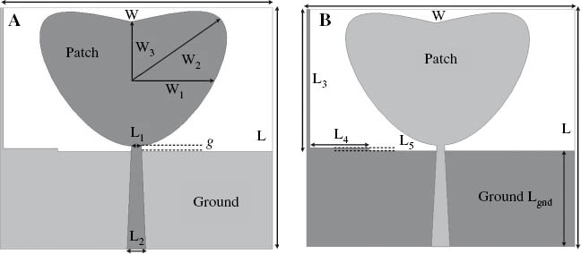
The reported antenna layout: (A) top view and (B) back view.
The surface current distribution on the ground plane and the patch of the proposed SWB antenna at frequencies 4, 8, 12, 18, and 20 GHz are illustrated in Figure 2. From Figure 2, it is observed that the L-type slit on the upper left portion of the ground plane plays an important role to create resonances and to achieve super frequency bands. This L-type slit has a major effect on all the frequencies. Besides, it can clearly be seen from Figure 2 that the microstrip feeding is a dominant figure, and the heart-shaped patch also plays a role in the flow current sharply. The direction of the current flow through the L-type slit is upward at frequencies 4 and 18 GHz and both upward and downward at 8, 12, and 20 GHz, respectively. As a result, SWB frequency is generated.

Surface current distribution of the proposed antenna at (A) 4 GHz, (B) 8 GHz, (C) 12 GHz, (D) 18 GHz, and (E) 20 GHz (F) scale.
3 Parametric analysis to patch and ground-related parameters
To provide antenna researchers, the parametric study is analyzed with more specific design properties. Electrical and geometrical parameters affect the performance of the antenna. In the simulation, all the parameters are kept constant without the desired parameter. All the simulations have been performed with the help of the 3-D electromagnetic simulator HFSS for parametric analysis.
The effects of varying feed shapes of the proposed SWB antenna are illustrated in Figure 3A. When we apply triangular feed with rectangular partial ground plane, it can be found that resonance starts from 1 GHz and there is an impedance mismatch at 6.8 GHz. When the rectangular feed line is used with the rectangular partial ground plane, lower frequency is shifted; on the other hand, over the operating frequency bands, the bandwidth is entirely affected. When a tapered feed line is applied with the rectangular partial ground plane, it delivers a well-matched impedance, which is from 1.25 to more than 20 GHz. The rectangular partial ground plane and the heart-shaped patch containing a gap are tuned properly for matching the impedance, and as a result, the working frequency band is increased, as shown in Figure 3B. The feed gap g acts very sensitive in the impedance matching. It can be observed from Figure 3B that lower frequency is shifted if the gap is reduced, and some resonances are found above VSWR line 2. However, g=0.97 mm is considered as optimum value.

Effects of (A) varying feed shapes. (B) Gap g other parameters are fixed.
The effects of varying the upper feed width on the heart-shaped patch are shown in Figure 4. It is found that lower frequency is shifted to lower end by increasing the optimum value; however, by decreasing the optimum value, VSWR is reduced at higher frequencies. Therefore, the optimum value 1.1 mm is considered.

Effects of varying the upper feed width on the heart-shaped radiating patch.
From Figure 5, four important parameters, such as the number of L-type slit, L-type slit horizontal length, L-type slit vertical length, and L-type slit width, can be observed. It can be seen from Figure 5 that if the L-type slit is not used, lower resonance is shifted and two resonances do not follow VSWR <2 on the higher frequency. If two L-type slits are applied on the two sides of the partial ground plane, VSWR is reduced over the operating bands. The proposed L-type slit is located on the left side of the ground plane. In the parametric analysis, the horizontal length of the L-type slit is taken as the value of 12, 11, 10, 9, and 8 mm. However, impedance can be tuned properly using 10 mm. Therefore, 10 mm is the optimum value of L-type slit horizontal length, as shown in Figure 5B. In the parametric analysis, the L-type slit vertical length is taken as 23.85, 19.85, 15.85, 13.85, and 8.85 mm. However, impedance can be tuned properly using 23.85 mm. Therefore, 23.85 mm is the optimum value of horizontal length L-type slit vertical length, as shown in Figure 5C. In the parametric analysis, the horizontal length L-type slit width is taken as 0, 0.25, 0.5, 1, and 1.5 mm. However, impedance can be tuned properly using 0.5 mm. Therefore, 0.5 mm is the optimum value of horizontal length L-type slit width, as shown in Figure 5D.

Effects of varying ground plane-related parameters: (A) number of L-type slit, (B) L-type slit horizontal length, (C) L-type slit vertical length, and (D) L-type slit width.
4 Frequency domain performance
The execution of the reported SWB antenna is optimized using electromagnetic simulator HFSS depending on the finite element method. The fabricated photograph of this reported antenna is indicated in Figure 6.

The photograph of the proposed SWB antenna prototype.
The measured results were obtained using the Agilent N5227A (10 MHz-67 GHz) PNA network analyzer. The variations between measured as well as simulated VSWR curves are demonstrated in Figure 7. The simulated impedance bandwidth covers 1.25 to more than 40 GHz frequency, where the measured impedance bandwidth covers 1.30 to more than 40 GHz frequency.

Comparison between simulated and measured VSWR of the proposed antenna.
The measured gain of this reported SWB antenna has been plotted in Figure 8. It can be observed from Figure 8 that this antenna provides an average peak gain of 4.10 dBi, where the maximum peak gain is 6.06 dBi at 11.45 GHz and the minimum peak gain is 2.20 dBi at 1.30 GHz. From starting, a rising gain is achieved until 6 GHz, then gain decreases and again increases with small fluctuation over the operating frequencies.

Measured gain of this reported antenna.
The measured normalized radiation pattern of the proposed SWB antenna is illustrated in Figure 9 for (A) 4 GHz, (B) 8 GHz, (C) 12 GHz, and (D) 16 GHz on the both E-plane and H-plane, respectively. Cross polarization is lower than copolarization, which is the characteristic of standard radiation pattern. It is observed that the proposed SWB antenna exhibits better broadside radiation features and considerable front-to-back ratio with low cross polarization, which leads to bidirectional and nearly omnidirectional radiation pattern along both the E-plane and the H-plane.

Measured radiation pattern at (A) 4 GHz, (B) 8 GHz, (C) 12 GHz, and (D) 16 GHz.
5 Time domain performance
We have accomplished a study depending on the CST Microwave Studio of full-wave simulation to realize this reported antenna’s time domain performance. Several studies [18], [19], [20], [21], [22] are adopted for the analysis. An input pulse of fourth-order Rayleigh is used, which adopts the following form plotted in Figure 10:

The input pulse with τ=67 ps.
The correlation coefficient between the transmitted signal and the received signal can illustrate the amount of pulse distortion, which is induced through the antenna. The fidelity factor (F) is defined using Equation (1) narrated in [19], [21], [22]:
where s(t) is the transmitted signal and r(t) is the received signal. For impulse radio in UWB communications, a high degree of correlation has to exist between the transmitted and the received signals to avoid losing the modulated information. However, it is not mandatory for most other telecommunication systems having the fidelity factor. The time domain performance of the proposed fractal UWB antenna is also performed. Three configurations, that is, face-to-face, side-by-side Y direction, and side-by-side X direction orientations, are chosen.
From the transmitting to receiving antenna, a narrow pulse was delivered at a distance of 300 mm from the transmitter, and then the received pulse was calculated. Figure 11 illustrates pulse transmission analysis in different orientations of the proposed antenna. The normalization between the transmitted pulse and the received pulse has been performed by their maximum level. This graph points out the negligible pulse distortion with respect to the peak value of 1. The fidelity factor is 0.84 for the face-to-face, 0.88 for side-by-side Y direction, and 0.71 for side-by-side X direction configurations, respectively. As a result, this proposed antenna supports less narrow pulse distortion for operation.

Pulse transmission analysis in different orientations of the proposed SWB antenna.
The group delay has been measured with the two identically designed antennas located face to face at a distance of 0.5 m apart, which delivers an indication of the time delay of a signal at different frequencies. It can be realized from Figure 12 that the proposed SWB antenna has been attained a stable group delay over the operating frequency bands. The small variation in group delay ensures that the reported SWB antenna has good linear transmission function properties.
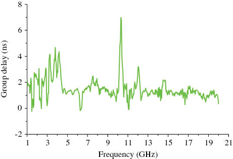
Measured group delay of the proposed antenna.
The measured phase variation of the input impedance has been illustrated in Figure 13. It can be found from the Figure 13 that the phase variation of the proposed SWB antenna is linear across the entire operating frequency bands. All the frequency components of the signal have the identical delay, which has been confirmed with this linear variation, including frequency in the phase, which leads to the same pulse distortion.

Measured phase value of the input impedance.
6 BDR comparison
With a view to authorizing the compactness of SWB antenna, the most formal method is to make comparison in their respective electrical dimension against the other antenna. However, each published SWB/UWB antenna is unique in the open literature, and their measured bandwidth would not be accurately the same along the 10-dB return loss and would not indicate that their originating frequencies (low-end frequency) are most probably improper. Unlike the UWB antenna that conducts a standard operating bandwidth that originates at 3.1 GHz, so that most of the authors can mention this frequency as the corresponding electrical dimension of their UWB antenna, the SWB antenna does not receive such an operating band standard. However, to provide an equitable comparison between two wideband antennas (particularly SWB and UWB antenna), the authors [5] have defined a new index term that will allow antenna engineers to identify if their planar antenna design (compared against the other design) is very much compact in size and wide in bandwidth. To ascertain both the wideband and the compactness characteristics of a planar antenna, an antenna index term called BDR has been initiated. This index term will indicate how much operating bandwidth (in percentage) can be provided per electrical area unit. This equation can be written as follows:
where λ is the wavelength of the working frequency at the lower end. Here, a larger BDR would announce that the design antenna is wider in bandwidth and smaller in dimension. In Equation (3), the relative permittivity of the antenna substrate is not taken into account. Two conditions such as printed type (planar) antenna and small differences in the substrate’s relative permittivity for the validity in comparison with the tightness among wideband antennas using the BDR can be authentic. To confirm reasonable difference between this reported antenna and the antennas mentioned on several studies [2], [5], [6], [7], [8], [9], [10], [11], [12], [13], [14], [15], their performances are listed in Table 1, such as ratio bandwidth, BDR, electrical dimension, and 10-dB bandwidth.
BDR comparisons among existing antennas with other parameters.
| Antennas | Bandwidth ratio | 10-dB bandwidth (%) | Electrical dimension | BDR | Flow (GHz) |
|---|---|---|---|---|---|
| [2] | 21.9:1 | 182.51 | 0.24 λ×0.38 λ | 1973.61 | 0.7986 |
| [5] | 13.1:1 | 171.54 | 0.17 λ×0.37 λ | 2762.66 | 1.44 |
| [6] | 32:1 | 187.88 | 0.33 λ×0.25 λ | 2254.55 | 2.50 |
| [8] | 9.11:1 | 160.45 | 0.35 λ×0.41 λ | 1122.70 | 3.50 |
| [7] | 5:1 | 133.33 | 2.00 λ×2.00 λ | 33.33 | 10.00 |
| [9] | 20.4:1 | 181.32 | 0.23 λ×0.33 λ | 2461.50 | 2.18 |
| [10] | 31.14:1 | 187.56 | 0.26 λ×0.28 λ | 2586.26 | 1.05 |
| [11] | 25:1 | 185.00 | 0.32 λ×0.34 λ | 1690.20 | 0.64 |
| [12] | 14.5:1 | 174.00 | 0.22 λ×0.22 λ | 3572.76 | 2.76 |
| [13] | 10.16:1 | 164.15 | 0.31 λ×0.46 λ | 1138.77 | 3.10 |
| [15] | 10.13:1 | 164.05 | 0.24 λ×0.33 λ | 2083.90 | 2.40 |
| [14] | 15.3:1 | 175.58 | 0.18 λ×0.22 λ | 4261.01 | 1.30 |
| Proposed | 30.77:1 | 187.41 | 0.17 λ×0.20 λ | 5544.65 | 1.30 |
7 Conclusion
A microstrip line-fed monopole antenna has been presented for SWB applications printed on epoxy-resin-reinforced woven-glass material. A parametric analysis with electromagnetic simulator and a design evolution have been performed. A tapered feed line with a heart-shaped patch and a rectangular partial ground has been used for enhancing the working bandwidth. The ground plane and the patch containing a gap and an L-type slit are also considered to attain the wide bandwidth. The proposed SWB antenna is fabricated on low dielectric FR4 material with the overall dimension of 0.17 λ×0.20 λ at 1.30 GHz lower frequency. The measurement results exhibit that the reported antenna acquires SWB covering from 1.30 to more than 20 GHz (187.41%). BDR is used for the accuracy of the compactness of this reported SWB antenna (BDR=5544.65). The nearly omnidirectional radiation patterns, low profile, stable gain (4.10 dBi), sharply surface current distribution, signal analysis, and small dimension characteristics of the proposed antenna provide the validation that the reported antenna is a promising candidate for SWB applications.
Acknowledgments
This work was supported by the Deanship of Scientific Research (DSR) at King Abdulaziz University, Jeddah, Saudi Arabia under grant no. 3-135-35-RG.
References
[1] Federal Communications Commission. Federal Communications Commission Revision of Part 15 of the Commission’s Rules Regarding Ultra-Wideband Transmission System from 3.1 to 10.6 GHz, Washington, DC, 2002, pp. 98–153.Search in Google Scholar
[2] Barbarino S, Consoli F. IEEE Trans. Antennas Propag. 2010, 58, 4074–4078.10.1109/TAP.2010.2078469Search in Google Scholar
[3] Lau K, Kong KC, Luk KM. Electron. Lett. 2008, 44, 716–718.10.1049/el:20080866Search in Google Scholar
[4] Jin X-H, Huang X-D, Cheng C-H, Zhu L. Prog. Electromagn. Res. Lett. 2011, 27, 117–123.10.2528/PIERL11090506Search in Google Scholar
[5] Chen K-R, Sim C, Row J-S. IEEE Antennas Wireless Propag. Lett. 2011, 10, 488–491.10.1109/LAWP.2011.2157071Search in Google Scholar
[6] Manohar M, Kshetrimayum RS, Gogoi AK. IET Microwaves Antennas Propag. 2014, 8, 39–45.10.1049/iet-map.2013.0094Search in Google Scholar
[7] Azari A. IEEE Trans. Antennas Propag. 2011, 59, 1724–1727.10.1109/TAP.2011.2128294Search in Google Scholar
[8] Srifi MN, Podilchak SK, Essaaidi M, Antar YM. IEEE Trans. Antennas Propag. 2011, 59, 4470–4480.10.1109/TAP.2011.2165503Search in Google Scholar
[9] Dorostkar MA, Islam MT, Azim R. Prog. Electromagn. Res. 2013, 139, 229–245.10.2528/PIER13030505Search in Google Scholar
[10] Liu J, Esselle K, Hay S, Zhong S. Electron. Lett. 2013, 49, 515–516.10.1049/el.2012.4015Search in Google Scholar
[11] Dong Y, Hong W, Liu L, Zhang Y, Kuai Z. Microwave Opt. Technol. Lett. 2009, 51, 949–956.10.1002/mop.24222Search in Google Scholar
[12] Akbari M, Koohestani M, Ghobadi C, Nourinia J. Microwave Opt. Technol. Lett. 2011, 53, 1481–1483.10.1002/mop.26090Search in Google Scholar
[13] Hakimi S, Rahim SKA, Abedian M, Noghabaei SM, Khalily M. IEEE Antennas Wireless Propag. Lett. 2014, 13, 1251–1254.10.1109/LAWP.2014.2333091Search in Google Scholar
[14] Samsuzzaman M, Islam M. Microwave Opt. Technol. Lett. 2015, 57, 445–452.10.1002/mop.28872Search in Google Scholar
[15] Chao D, Yong-jun X, Ping L. IEEE Antennas Wireless Propag. Lett. 2009, 8, 1394–1397.10.1109/LAWP.2009.2039743Search in Google Scholar
[16] Ullah MH, Islam MT, Mandeep J, Misran N. Sci. Eng. Compos. Mater. 2014, 21, 405–410.10.1515/secm-2013-0149Search in Google Scholar
[17] Faruque MRI, Islam MT, Mohamed NAN. Sci. Eng. Compos. Mater. 2014, 21, 79–85.10.1515/secm-2013-0044Search in Google Scholar
[18] Chen ZN, Wu XH, Li HF, Yang N, Chia MYW. IEEE Trans. Antennas Propag. 2004, 52, 1739–1748.10.1109/TAP.2004.831405Search in Google Scholar
[19] Quintero G, Zurcher J-F, Skriverviky A. IEEE Trans. Antennas Propag. 2011, 59, 2502–2512.10.1109/TAP.2011.2152322Search in Google Scholar
[20] Mehdipour A, Mohammadpour-Aghdam K, Faraji-Dana R, Kashani-Khatib M-R. IEEE Trans. Antennas Propag. 2008, 56, 3857–3862.10.1109/TAP.2008.2007401Search in Google Scholar
[21] Islam M, Islam M, Samsuzzaman M, Faruque M, Misran N, Mansor M. Materials 2015, 8, 392–407.10.3390/ma8020392Search in Google Scholar PubMed PubMed Central
[22] Islam MT, Islam MM, Samsuzzaman M, Faruque MRI, Misran N. Sensors 2015, 15, 11601–11627.10.3390/s150511601Search in Google Scholar PubMed PubMed Central
©2017 Walter de Gruyter GmbH, Berlin/Boston
This article is distributed under the terms of the Creative Commons Attribution Non-Commercial License, which permits unrestricted non-commercial use, distribution, and reproduction in any medium, provided the original work is properly cited.
Articles in the same Issue
- Frontmatter
- Original articles
- Wave propagation in functionally graded piezoelectric-piezomagnetic rectangular bars
- Graphene/poly(vinylidene fluoride) dielectric composites with polydopamine as interface layers
- A novel biaxial double-negative metamaterial for electromagnetic rectangular cloaking operation
- Formation of homogenous copper film on MWCNTs by an efficient electroless deposition process
- Nano-SiCp/Al2014 composites with high strength and good ductility
- Microstrip line-fed monopole antenna on an epoxy-resin-reinforced woven-glass material for super wideband applications
- Influence of casting speed on fabricating Al-1%Mn and Al-10%Si alloy clad slab
- Thermal insulating epoxy composite coatings containing sepiolite/hollow glass microspheres as binary fillers: morphology, simulation and application
- Analysis of influence of fibre type and orientation on dynamic properties of polymer laminates for evaluation of their damping and self-heating
- Dynamic stability of nanocomposite viscoelastic cylindrical shells coating with a piezomagnetic layer conveying pulsating fluid flow
- Buckling and layer failure of composite laminated cylinders subjected to hydrostatic pressure
- One-step preparation and characterization of core-shell SiO2/Ag composite spheres by pulse plating
- The failure mechanism of carbon fiber-reinforced composites under longitudinal compression considering the interface
- A thermal-plastic model of friction stir welding in aluminum alloy
- A model for longitudinal tensile strength prediction of low braiding angle three-dimensional and four-directional composites
- Nonlinear stability of shear deformable eccentrically stiffened functionally graded plates on elastic foundations with temperature-dependent properties
- Design and multibody dynamics analyses of the novel force-bearing structures for variable configuration spacecraft