High-efficiency generation of far-field spin-polarized wavefronts via designer surface wave metasurfaces
-
Weikang Pan
 ,
Lei Zhou
,
Lei Zhou
 und
Shulin Sun
und
Shulin Sun

Abstract
Achieving a pre-designed scattering pattern from an ultra-compact platform is highly desired for on-chip integration optics, but conventional techniques suffer from the limitations of bulky size, wavelength-scale modulation and low efficiency. Here, we propose a new strategy to efficiently generate arbitrary spin-polarized scattering far-field patterns from surface-wave (SW) excitations on a designer Pancharatnam–Berry (PB) metasurface. We find that a PB meta-atom serves as a subwavelength scatter to decouple impinging SW to a spin-polarized propagating wave (PW) with tailored amplitude and phase, and thus interference among PWs generated by scatterings at different PB meta-atoms can generate a tailored far-field pattern. As a proof of concept, we design and fabricate a series of PB metasurfaces in the microwave regime and experimentally demonstrate that they can generate desired radiation patterns within a broad frequency band, including unidirectional radiation, line/point focusing, vortex beam and hologram. These findings may stimulate important applications in on-chip integrated photonics.
1 Introduction
Surface waves (SWs) are eigen electromagnetic (EM) modes bounded at dielectric/metal surfaces [1], [2], [3]. Due to subwavelength resolution and local-field enhancement characteristics, SWs can find numerous applications in integration-optics, such as sub-diffraction imaging [4, 5], sensing [6, 7], plasmonic laser [8], [9], [10], [11], on-chip plasmonic circuit [12], [13], [14], [15], and enhanced nonlinear optics [16, 17]. In these applications, a crucial issue is to find appropriate devices to efficiently couple impinging propagating waves (PWs) into SWs inside the on-chip devices. Conventional PW–SW couplers, such as prism couplers [18, 19], grating couplers [20] and fibers coupler [21, 22], are bulky and less efficient. Recently, gradient metasurfaces exhibiting reflection/transmission phases linearly varying in space were found as efficient PW–SW couplers [23]. Different types of meta-couplers were proposed and experimentally characterized, working in reflection [24], [25], [26], [27] or transmission mode [28, 29], under excitations of PWs with linear or circular polarizations. Integrated with active elements, the metasurfaces can further exhibit tunable or reprogrammable functionality to manipulate impinging waves [30, 31].
On the other hand, achieving pre-designed far-field radiations from SWs flowing on a planar device have attracted much attention from science and technology recently. Scatterings of SWs by small objects/apertures usually generate significant beam divergence [10]. To address this issue, Lezec et al. added periodic textures surrounding a small aperture in a metal film to help collimate light beam emerged from the aperture, based on Bragg interferences of waves emitted through SW scatterings at these periodic structures [32]. Such a strategy was further applied to realize edge-emitting-semiconductor lasers with small angular divergence [33, 34]. Utilizing such a scheme, more fascinating beam-control effects were demonstrated with SW excitations on flat devices, such as far-field focusing [35], [36], [37], Airy beam [38, 39] and vortex beam [39], and holograms [40], [41], [42], [43]. Such an approach can find numerous promising applications in future on-chip optics, such as planar antenna [44, 45], mini-projector [46], [47], [48], and virtual reality displays [49].
However, these Bragg-type devices suffer from several limitations. Taking the Bragg grating as an example (see Figure 1A), while scatterings of an SW flowing across such a device can form a linearly polarized main beam in the far-field due to constructive interference, high-order beams may also be formed which degrades the performance of the device (see numerical demonstrations in Section A of Supplementary Material). The key issue is that Bragg devices can only control the scattered waves at the wavelength scale, but cannot control the amplitude, phase and polarization of wave scatterings at the deep-subwavelength scale, which significantly limit their abilities to freely engineer the far-field radiations.
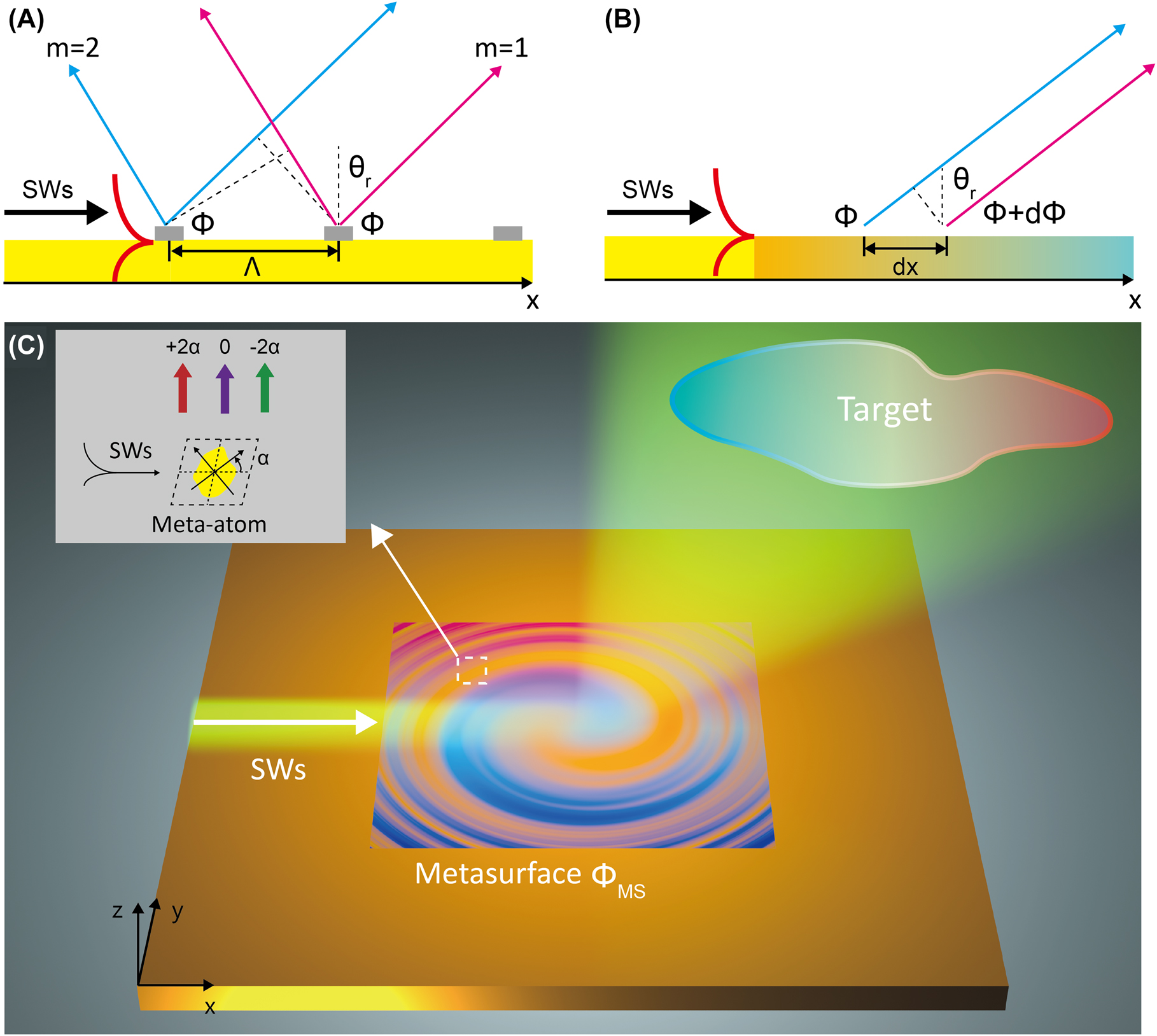
Schematics to illustrate physical concept of SW–PW radiations.
(A) Physical concept of SW–PW radiations with Bragg structure. Based on Bragg scattering, the SWs are decoupled into different PW modes with the blue and red lines representing two out-going optical paths emitted by adjacent structures. (B) Physical concept of SW–PW radiations via the phase gradient provided by gradient metasurface. (C) Arbitrary scattering far-field patterns enabled by SWs decoupling with gradient metasurface. As shown in the inset, three different scattering mode are excited inside the meta-atom (of an orientation angle
In this paper, we propose a new strategy to achieve arbitrary spin-polarized far-field scattering patterns based on metasurfaces. Injecting an SW to excite a carefully designed PB meta-device (see Figure 1C), each meta-atom inside the device can serve as a subwavelength scatter to convert incident SW to circularly polarized PW with amplitude and phase determined by the structure and orientation of local meta-atom. Interferences among those scattered waves can form a desired far-field wavefront. We use this strategy to design/fabricate a series of microwave meta-devices and experimentally demonstrate various far-field scattering patterns, including unidirectional emission, focusing, vortex beam, and hologram. Compared to Bragg-type devices, our strategy exhibits the merits of single-mode operation, high-efficiency, high-resolution and being able to realize spin-polarized beams.
2 Physical concept and meta-atom design
Consider that an impinging SW with transvers-magnetic (TM) polarization travels across a carefully designed PB metasurface (see Figure 1B). As the impinging SW hits a PB meta-atom, electromagnetic resonances of meta-atom can be excited. Assuming that the meta-atom is deep-subwavelength in size and neglecting the spatial variation of
As a particular example, we illustrate how to design the PB meta-device aiming to realize the directional far-field radiation (see Figure 1B) with left circular polarization (LCP). To determine the
where
As a proof of concept, we choose the microwave regime to demonstrate our idea. Figure 2A depicts the proposed/fabricated PB meta-atom in metal–insulator–metal (MIM) configuration, consisting of an H-shaped copper resonator and a copper thin film separated by a 2 mm-thick F4B dielectric spacer

Characterizations of the designed PB meta-atoms and plasmonic system.
(A) Picture of the fabricated PB meta-atoms composed by the copper H-shaped resonator and a copper film that are separated by a dielectric spacer
3 Unidirectional far-field radiation
We now investigate the unidirectional far-field emission from SW excitations on the gradient PB metasurface, as illustrated in Figure 3A. We first design a “plasmonic metal” supporting eigen SWs, so that an impinging SW can be excited as the source. Without causing too much undesired scatterings, the “plasmonic metal” that we design is simply a metallic ground plane covered by a dielectric spacer of the same thickness as that of the PB meta-atom (see inset to Figure 2D). Dispersion relation of SWs supported by such a structure can be computed analytically, which is further verified by our near-field experimental measurements on a realistic sample (see Figure 2D). Choosing the working frequency as 12 GHz, we find that our “plasmonic metal” supports an eigen SW with

Characterizations of SW–PW unidirectional radiation based on PB metasurface.
(A) Schematic of the plasmonic metal (left) and PB metasurface with a linear phase profile (right) for SW–PW radiation. (B) Measured E x field distribution of the sample (see bottom figure) for SW–PW radiation at 12 GHz, obtained by the near-field mapping technique. The inset figure illustrates the simulated (blue line) and measured (red open circles) scattered far-field angular distribution at 12 GHz. (C) and (D) The scattered far-field intensities of (C) LCP and (D) RCP radiated by our device as functions of radiation angle and frequency.
We experimentally characterize the polarization state of the generated beam. Adopting the LCP antenna as the receiver, we find that the measured normalized angular distributions of scattered field agree very well with theoretical prediction given by Eq. (1) (see pink solid line in Figure 3C), exhibiting nice single-mode emission within the frequency band (11–15 GHz). As we change to use the RCP receiver antenna, we cannot collect any far-field emissions (see Figure 3D). These findings undoubtedly demonstrate that the out-going PW generated by our PB device carries a pure LCP. Moreover, the polarization characteristic the radiated PW beam can be well controlled by changing the orientation sequence of PB meta-atoms in the device (see Section E in Supplementary Material).
We can freely modulate the radiation direction covering the full angle range (

Verification of SW–PW unidirectional radiation covering full radiation angle.
(A) Sample images of two meta-devices with different phase gradients:
We discuss how the PCR of the constituent meta-atom influences the performance of PB meta-device. We design five different PB meta-atoms exhibiting distinct PCR values at the frequency 12 GHz, via simply tuning the parameter
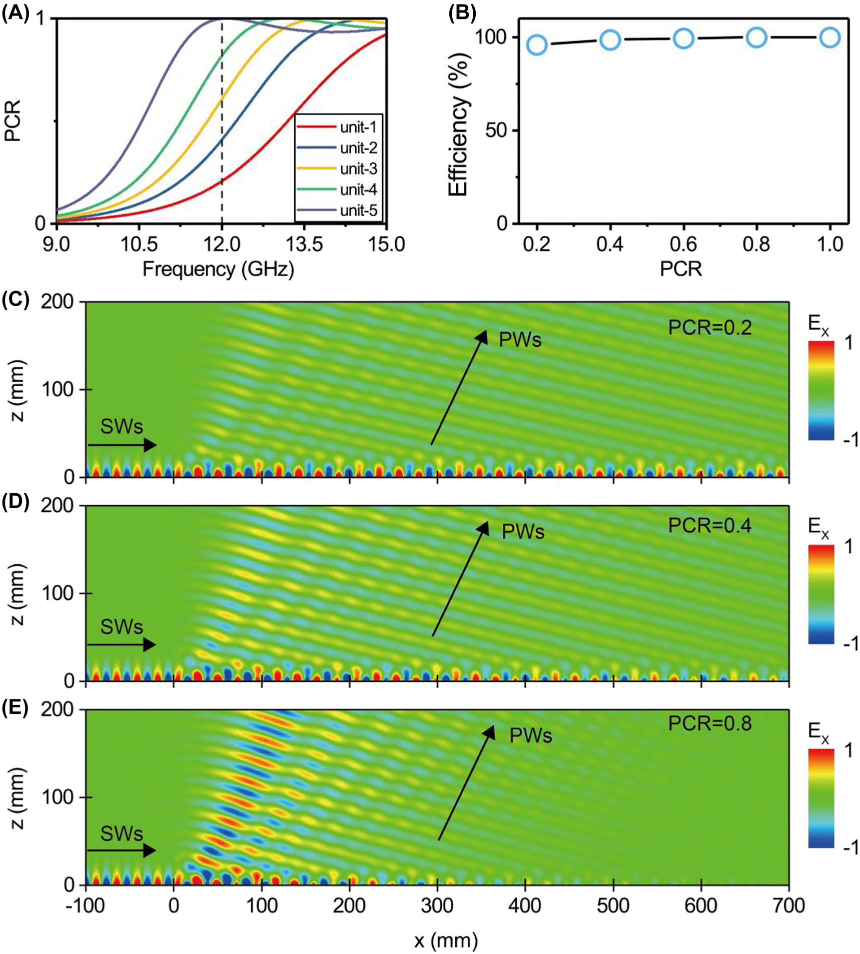
Decoupling speed and conversion efficiency of SW–PW radiation based on PB metasurfaces of different PCRs.
(A) PCR as a function of frequency for five different PB unit structures with different l 2 (l 2 = 1.6, 2.0, 2.25, 2.5, 2.9 mm). All of the other parameters are totally same to those of the meta-atoms in Figure 2A. (B) Conversion efficiency of SW–PW radiation as a function of PCR for the adopted PB metasurface, computed based on full wave simulations. (C)–(E) Simulated E x field distribution of SW–PW radiation with PB metasurface of the same phase gradient but different PCRs (i.e., 0.2, 0.4, 0.8). Here, the metadevice consists of 150 meta-atoms (i.e., 720 mm), which is long enough to decouple all impinging SWs.
We discuss an important advantage of our metasurface-based scheme to achieve pre-designed far-field scattering patterns. As shown in previous discussions, meta-atoms inside our PB meta-devices can control not only the phases of locally scattered waves (dictated by the orientation angles of meta-atoms), but also the amplitudes of such waves (dictated by the PCR values of meta-atoms), all in deep-subwavelength scale. It has been shown (see Figure 5E) that the generated far-field beam does not exhibit a flat wavefront in the large-PCR meta-atom case. This can be remedied by slightly adjusting the meta-atoms structures at different locations (see numerical demonstration in Figure S7 of Supplementary Material), so that their SW–PW scattering capabilities (related to their PCR values) can compensate the decrement in local SW strength due to scattering losses of SW flowing on the device surface. Such local-control capabilities on both phase and amplitude offer us possibilities to manipulate the far-field radiation patterns as desired with deep-subwavelength resolution, which can find numerous photonic applications [58].
4 Arbitrary scattering far-field patterns
We use the proposed strategy to demonstrate other meta-devices to achieve more complicated scattering far-field patterns. The first example is line focusing as depicted in Figure 6A. Based on the similar analyses as in Section 2, we find that the phase profile of the PB meta-device
where
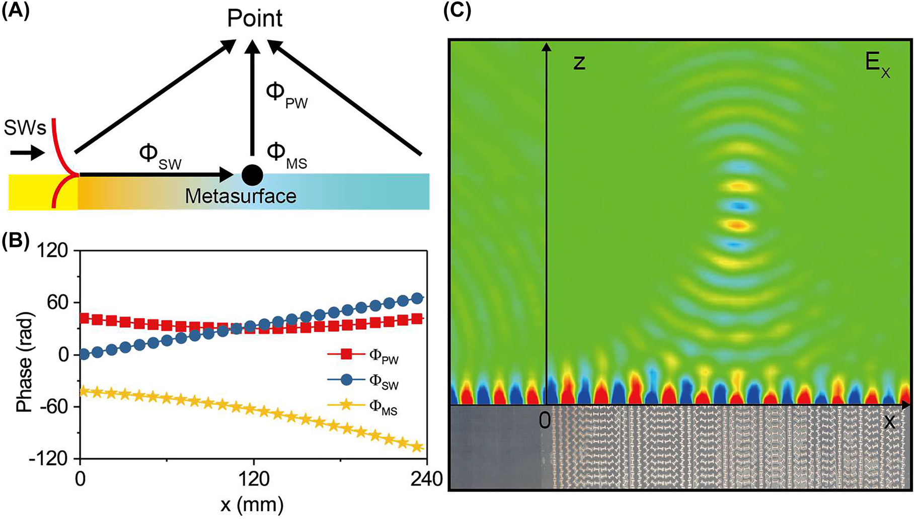
Far-field line focusing of SWs decoupled by the metasurface.
(A) Schematic of line focusing effect of SW–PW radiation with metasurface. (B) Three parts of phases, i.e., the propagation phase of SWs on metasurface
We use the proposed strategy to further demonstrate, both numerically and experimentally, three different meta-devices, that can generate far-field scattering patterns including three-dimensional (3D) focusing, vortex beam and hologram (see Figure 7), respectively. Based on the same analyses, we find that the phase profiles of these devices should satisfy
respectively.

Complicated scattering far-field patterns with PB metasurfaces.
(A), (D), (G) Far-field 3D focusing, (B), (E), (H) vortex beam and (C), (F), (I) hologram are generated by different SW metasurfaces according to Eq. (3). Scattered far-field patterns (on x–y plane) excited by SWs with three different PB metasurfaces, obtained by (D)–(F) experimental measurements and (G)–(I) full wave simulations. (A)–(C) The phase profiles of PB metasurfaces to achieve three functionalities. Here, the frequency is fixed at 12 GHz.
We design and fabricate the first meta-device for achieving 3D focusing (with F = 120 mm and L = 240 mm) with
We next design the second meta-device based on the phase profile shown in Eq. (3b), which is expected to generate a vortex beam exhibiting orbital angular momentum (OAM) with a topological charge q = 2. Here, different from the first device, we have individually designed meta-atoms at different locations to make them exhibit particular PCR values, so that locally scattered waves can roughly exhibit the same amplitude. In addition, lattice spacing between adjacent PB meta-atoms is also reduced to improve the subwavelength properties. Figure 7B depicts the desired phase distribution possessed by the meta-device. We then fabricate the device and experimentally characterize its functionality at 12 GHz. Measured E x field distribution on the plane of z = 400 mm clearly demonstrates the OAM beam generation with q = 2, which also agrees well with FDTD simulation results (see Figure 7E and H).
Our scheme is so generic that we can also use it to realize holographic images in free space, with meta-devices exhibiting carefully designed phases (see Eq. (3c)). As a proof of concept, we design the third meta-device to realize a free-space image of a letter ‘F’ on the plane of z = 120 mm, as the device is excited by an SW at 12 GHz. To achieve this goal, we first adopt the Gerchberg–Saxton (GS) algorithm [59], [60], [61] to retrieve the PB phase distribution
5 Conclusions
In this work, we propose a generic strategy to design PB meta-devices for achieving spin-polarized far-field scattering wavefronts, and experimentally verify the concept in the microwave regime. Under SW excitations, carefully designed PB meta-atoms can scatter impinging SWs to spin-polarized free-space waves with tailored amplitudes and phases, and thus their interference can form arbitrary scattering far-field patterns in subwavelength scales. A series of meta-devices are designed, fabricated and characterized, which can realize far-field patterns including unidirectional emission, 2D and 3D focusing, OAM beam and hologram. Compared to other meta-devices for controlling PWs based on PW excitations [24, 62], present meta-devices show the advantages of high-integration and high-efficiency, which are highly desired for future on-chip photonic applications. However, different local fields experienced by different meta-atoms inside device also obviously increase the complexity in designing these meta-devices. After realizing high-efficiency PW-SW coupling in our previous works [24, 63], we have finally achieved the two-way conversions between PW and SW, significantly expanding our capabilities to manipulate EM waves. Such a concept is quite generic that can be further developed to high frequency regimes. Our findings may inspire important applications in integration optics, such as leaky antenna, virtual reality imaging, plasmonic micro projector, virtual reality displays, etc., and realizing them in different frequency regimes are interesting future projects.
Funding source: Shanghai Science and Technology Committee
Award Identifier / Grant number: 20JC1414601
Funding source: National Natural Science Foundation of China
Award Identifier / Grant number: 11874118, 91850101, 11734007, 62192771
Funding source: National Key Research and Development Program of China
Award Identifier / Grant number: 2020YFA0710100, 2017YFA0303504
Funding source: Fudan University-CIOMP Joint Fund
Award Identifier / Grant number: FC2018-008
-
Author contribution: All the authors have accepted responsibility for the entire content of this submitted manuscript and approved submission.
-
Research funding: This work was supported by National Key Research and Development Program of China (2020YFA0710100, 2017YFA0303504), National Natural Science Foundation of China (Nos. 11874118, 91850101, 11734007, 62192771), and Shanghai Science and Technology Committee (Grant No. 20JC1414601), and Fudan University-CIOMP Joint Fund (No. FC2018-008).
-
Conflict of interest statement: The authors declare no conflicts of interest regarding this article.
References
[1] W. L. Barnes, A. Dereux, and T. W. Ebbesen, “Surface plasmon subwavelength optics,” Nature, vol. 424, pp. 824–830, 2003. https://doi.org/10.1038/nature01937.Suche in Google Scholar PubMed
[2] J. B. Pendry, L. Martín-Moreno, F. J. Garcia-Vidal, L. Martin-Moreno, and F. J. Garcia-Vidal, “Mimicking surface plasmons with structured surfaces,” Science, vol. 305, pp. 847–848, 2004. https://doi.org/10.1126/science.1098999.Suche in Google Scholar PubMed
[3] S. A. Maier, Plasmonics: Fundamentals and Applications, US: Springer, 2007.10.1007/0-387-37825-1Suche in Google Scholar
[4] J. B. Pendry, “Negative refraction makes a perfect lens,” Phys. Rev. Lett., vol. 85, pp. 3966–3969, 2000. https://doi.org/10.1103/physrevlett.85.3966.Suche in Google Scholar PubMed
[5] N. Fang, H. Lee, C. Sun, and X. Zhang, “Sub-diffraction-limited optical imaging with a silver superlens,” Science, vol. 308, pp. 534–537, 2005. https://doi.org/10.1126/science.1108759.Suche in Google Scholar PubMed
[6] J. N. Anker, W. P. Hall, O. Lyandres, et al.., “Biosensing with plasmonic nanosensors,” Nat. Mater., vol. 7, pp. 442–453, 2008. https://doi.org/10.1038/nmat2162.Suche in Google Scholar PubMed
[7] S. Zhang, K. Bao, N. J. Halas, H. Xu, and P. Nordlander, “Substrate-induced fano resonances of a plasmonic nanocube: a route to increased-sensitivity localized surface plasmon resonance sensors revealed,” Nano Lett., vol. 11, pp. 1657–1663, 2011. https://doi.org/10.1021/nl200135r.Suche in Google Scholar PubMed
[8] D. Bergman and M. Stockman, “Surface plasmon amplification by stimulated emission of radiation: quantum generation of coherent surface plasmons in nanosystems,” Phys. Rev. Lett., vol. 90, p. 27402, 2003. https://doi.org/10.1103/physrevlett.90.027402.Suche in Google Scholar PubMed
[9] S. I. Azzam, A. V. Kildishev, R.-M. Ma, et al.., “Ten years of spasers and plasmonic nanolasers,” Light Sci. Appl., vol. 9, p. 90, 2020. https://doi.org/10.1038/s41377-020-0319-7.Suche in Google Scholar PubMed PubMed Central
[10] R. F. Oulton, V. J. Sorger, T. Zentgraf, et al.., “Plasmon lasers at deep subwavelength scale,” Nature, vol. 461, pp. 629–632, 2009. https://doi.org/10.1038/nature08364.Suche in Google Scholar PubMed
[11] H. Z. Chen, J. Q. Hu, S. Wang, et al.., “Imaging the dark emission of spasers,” Sci. Adv., vol. 3, 2017, Art no. e1601962. https://doi.org/10.1126/sciadv.1601962.Suche in Google Scholar PubMed PubMed Central
[12] V. J. Sorger, R. F. Oulton, R.-M. Ma, and X. Zhang, “Toward integrated plasmonic circuits,” MRS Bull., vol. 37, pp. 728–738, 2012. https://doi.org/10.1557/mrs.2012.170.Suche in Google Scholar
[13] S. I. Bozhevolnyi, V. S. Volkov, E. Devaux, J. Y. Laluet, and T. W. Ebbesen, “Channel plasmon subwavelength waveguide components including interferometers and ring resonators,” Nature, vol. 440, pp. 508–511, 2006. https://doi.org/10.1038/nature04594.Suche in Google Scholar PubMed
[14] H. Wei, Z. Wang, X. Tian, M. Käll, and H. Xu, “Cascaded logic gates in nanophotonic plasmon networks,” Nat. Commun., vol. 2, p. 387, 2011. https://doi.org/10.1038/ncomms1388.Suche in Google Scholar PubMed PubMed Central
[15] Y. Meng, Y. Chen, L. Lu, et al.., “Optical meta-waveguides for integrated photonics and beyond,” Light Sci. Appl., vol. 10, p. 235, 2021. https://doi.org/10.1038/s41377-021-00655-x.Suche in Google Scholar PubMed PubMed Central
[16] M. Kauranen and A. V. Zayats, “Nonlinear plasmonics,” Nat. Photonics, vol. 6, pp. 737–748, 2012. https://doi.org/10.1038/nphoton.2012.244.Suche in Google Scholar
[17] J. Shi, Y. Li, M. Kang, et al.., “Efficient second harmonic generation in a hybrid plasmonic waveguide by mode interactions,” Nano Lett., vol. 19, pp. 3838–3845, 2019. https://doi.org/10.1021/acs.nanolett.9b01004.Suche in Google Scholar PubMed
[18] A. Otto, “Excitation of nonradiative surface plasma waves in silver by the method of frustrated total reflection,” Z. Phys. A: Hadrons Nucl., vol. 216, pp. 398–410, 1968. https://doi.org/10.1007/bf01391532.Suche in Google Scholar
[19] M. J. Lockyear, A. P. Hibbins, and J. R. Sambles, “Microwave surface-plasmon-like modes on thin metamaterials,” Phys. Rev. Lett., vol. 102, 2009, Art no. 073901. https://doi.org/10.1103/PhysRevLett.102.073901.Suche in Google Scholar PubMed
[20] P. Lalanne, J. P. Hugonin, and J. C. Rodier, “Theory of surface plasmon generation at nanoslit apertures,” Phys. Rev. Lett., vol. 95, p. 263902, 2005. https://doi.org/10.1103/physrevlett.95.263902.Suche in Google Scholar
[21] R. F. Oulton, V. J. Sorger, D. A. Genov, D. F. P. Pile, and X. Zhang, “A hybrid plasmonic waveguide for subwavelength confinement and long-range propagation,” Nat. Photonics, vol. 2, pp. 496–500, 2008. https://doi.org/10.1038/nphoton.2008.131.Suche in Google Scholar
[22] X. Guo, M. Qiu, J. Bao, et al.., “Direct coupling of plasmonic and photonic nanowires for hybrid nanophotonic components and circuits,” Nano Lett., vol. 9, pp. 4515–4519, 2009. https://doi.org/10.1021/nl902860d.Suche in Google Scholar PubMed
[23] S. Sun, Q. He, J. Hao, S. Xiao, and L. Zhou, “Electromagnetic metasurfaces: physics and applications,” Adv. Opt. Photon., vol. 11, p. 380, 2019. https://doi.org/10.1364/aop.11.000380.Suche in Google Scholar
[24] S. Sun, Q. He, S. Xiao, et al.., “Gradient-index meta-surfaces as a bridge linking propagating waves and surface waves,” Nat. Mater., vol. 11, pp. 426–431, 2012. https://doi.org/10.1038/nmat3292.Suche in Google Scholar PubMed
[25] A. Pors, M. G. Nielsen, T. Bernardin, J.-C. Weeber, and S. I. Bozhevolnyi, “Efficient unidirectional polarization-controlled excitation of surface plasmon polaritons,” Light Sci. Appl., vol. 3, p. e197, 2014. https://doi.org/10.1038/lsa.2014.78.Suche in Google Scholar
[26] J. Duan, H. Guo, S. Dong, et al.., “High-efficiency chirality-modulated spoof surface plasmon meta-coupler,” Sci. Rep., vol. 7, p. 1354, 2017. https://doi.org/10.1038/s41598-017-01664-w.Suche in Google Scholar PubMed PubMed Central
[27] D. Wang, F. Liu, T. Liu, et al.., “Efficient generation of complex vectorial optical fields with metasurfaces,” Light Sci. Appl., vol. 10, p. 67, 2021. https://doi.org/10.1038/s41377-021-00504-x.Suche in Google Scholar PubMed PubMed Central
[28] L. Huang, X. Chen, B. Bai, et al.., “Helicity dependent directional surface plasmon polariton excitation using a metasurface with interfacial phase discontinuity,” Light Sci. Appl., vol. 2, p. e70, 2013. https://doi.org/10.1038/lsa.2013.26.Suche in Google Scholar
[29] W. Sun, Q. He, S. Sun, and L. Zhou, “High-efficiency surface plasmon meta-couplers: concept and microwave-regime realizations,” Light Sci. Appl., vol. 5, 2016, Art no. e16003. https://doi.org/10.1038/lsa.2016.3.Suche in Google Scholar PubMed PubMed Central
[30] Q. Ma, G. D. Bai, H. B. Jing, et al.., “Smart metasurface with self-adaptively reprogrammable functions,” Light Sci. Appl., vol. 8, p. 98, 2019. https://doi.org/10.1038/s41377-019-0205-3.Suche in Google Scholar PubMed PubMed Central
[31] J. W. You, Q. Ma, Z. Lan, et al.., “Reprogrammable plasmonic topological insulators with ultrafast control,” Nat. Commun., vol. 12, p. 5468, 2021. https://doi.org/10.1038/s41467-021-25835-6.Suche in Google Scholar PubMed PubMed Central
[32] H. J. Lezec, A. Degiron, E. Devaux, et al.., “Beaming light from a subwavelength Aperture,” Science, vol. 297, pp. 820–822, 2002. https://doi.org/10.1126/science.1071895.Suche in Google Scholar PubMed
[33] N. Yu, R. Blanchard, J. Fan, et al.., “Small divergence edge-emitting semiconductor lasers with two-dimensional plasmonic collimators,” Appl. Phys. Lett., vol. 93, p. 181101, 2008. https://doi.org/10.1063/1.3009599.Suche in Google Scholar
[34] N. Yu, J. Fan, Q. J. Wang, et al.., “Small-divergence semiconductor lasers by plasmonic collimation,” Nat. Photonics, vol. 2, pp. 564–570, 2008. https://doi.org/10.1038/nphoton.2008.152.Suche in Google Scholar
[35] H. Shi, C. Du, and X. Luo, “Focal length modulation based on a metallic slit surrounded with grooves in curved depths,” Appl. Phys. Lett., vol. 91, 2007, Art no. 093111. https://doi.org/10.1063/1.2776875.Suche in Google Scholar
[36] S. Kim, Y. Lim, H. Kim, J. Park, and B. Lee, “Optical beam focusing by a single subwavelength metal slit surrounded by chirped dielectric surface gratings,” Appl. Phys. Lett., vol. 92, 2008, Art no. 013103. https://doi.org/10.1063/1.2828716.Suche in Google Scholar
[37] M. S. Kumar, X. Piao, S. Koo, S. Yu, and N. Park, “Out of plane mode conversion and manipulation of surface plasmon polariton waves,” Opt. Express, vol. 18, pp. 8800–8805, 2010. https://doi.org/10.1364/oe.18.008800.Suche in Google Scholar
[38] X. M. Tang, L. Li, T. Li, et al.., “Converting surface plasmon to spatial Airy beam by graded grating on metal surface,” Opt. Lett., vol. 38, pp. 1733–1735, 2013. https://doi.org/10.1364/ol.38.001733.Suche in Google Scholar
[39] I. Dolev, I. Epstein, and A. Arie, “Surface-plasmon holographic beam shaping,” Phys. Rev. Lett., vol. 109, p. 203903, 2012. https://doi.org/10.1103/physrevlett.109.203903.Suche in Google Scholar
[40] M. Ozaki and S. K. Jun-ichi Kato, “Surface-plasmon holography with white-light illumination,” Science, vol. 332, pp. 218–220, 2011. https://doi.org/10.1126/science.1201045.Suche in Google Scholar PubMed
[41] Y.-H. Chen, L. Huang, L. Gan, and Z.-Y. Li, “Wavefront shaping of infrared light through a subwavelength hole,” Light Sci. Appl., vol. 1, p. e26, 2012. https://doi.org/10.1038/lsa.2012.26.Suche in Google Scholar
[42] J. Chen, T. Li, S. Wang, and S. Zhu, “Multiplexed holograms by surface plasmon propagation and polarized scattering,” Nano Lett., vol. 17, pp. 5051–5055, 2017. https://doi.org/10.1021/acs.nanolett.7b02295.Suche in Google Scholar PubMed
[43] T. Suhara, H. Nishihara, and J. Koyama, “Waveguide holograms: a new approach to hologram integration,” Opt. Commun., vol. 19, pp. 353–358, 1976. https://doi.org/10.1016/0030-4018(76)90097-3.Suche in Google Scholar
[44] J. J. Xu, H. C. Zhang, Q. Zhang, and T. J. Cui, “Efficient conversion of surface-plasmon-like modes to spatial radiated modes,” Appl. Phys. Lett., vol. 106, 2015, Art no. 021102. https://doi.org/10.1063/1.4905580.Suche in Google Scholar
[45] M. Wang, H. F. Ma, W. X. Tang, S. Sun, and T. J. Cui, “Leaky-wave radiations with arbitrarily customizable polarizations based on spoof surface plasmon polaritons,” Phys. Rev. Appl., vol. 12, 2019, Art no. 014036. https://doi.org/10.1103/physrevapplied.12.014036.Suche in Google Scholar
[46] C. M. Chang, M. L. Tseng, B. H. Cheng, et al.., “Three-dimensional plasmonic micro projector for light manipulation,” Adv. Mater., vol. 25, pp. 1118–1123, 2013. https://doi.org/10.1002/adma.201203308.Suche in Google Scholar PubMed PubMed Central
[47] Z. Huang, D. L. Marks, and D. R. Smith, “Out-of-plane computer-generated multicolor waveguide holography,” Optica, vol. 6, pp. 119–124, 2019. https://doi.org/10.1364/optica.6.000119.Suche in Google Scholar
[48] C. Yu, Y. Peng, Q. Zhao, H. Li, and X. Liu, “Highly efficient waveguide display with space-variant volume holographic gratings,” Appl. Opt., vol. 56, pp. 9390–9397, 2017. https://doi.org/10.1364/ao.56.009390.Suche in Google Scholar PubMed
[49] J. Xiong, E.-L. Hsiang, Z. He, T. Zhan, and S.-T. Wu, “Augmented reality and virtual reality displays: emerging technologies and future perspectives,” Light Sci. Appl., vol. 10, p. 216, 2021. https://doi.org/10.1038/s41377-021-00658-8.Suche in Google Scholar PubMed PubMed Central
[50] F. Guan, S. Sun, S. Xiao, Q. He, and L. Zhou, “Scatterings from surface plasmons to propagating waves at plasmonic discontinuities,” Sci. Bull., vol. 64, pp. 802–807, 2019. https://doi.org/10.1016/j.scib.2019.05.003.Suche in Google Scholar
[51] L. Huang, X. Chen, H. Mühlenbernd, et al.., “Dispersionless phase discontinuities for controlling light propagation,” Nano Lett., vol. 12, pp. 5750–5755, 2012. https://doi.org/10.1021/nl303031j.Suche in Google Scholar PubMed
[52] W. Luo, S. Xiao, Q. He, S. Sun, and L. Zhou, “Photonic spin Hall effect with nearly 100% efficiency,” Adv. Opt. Mater., vol. 3, pp. 1102–1108, 2015.10.1002/adom.201500068Suche in Google Scholar
[53] G. Zheng, H. Mühlenbernd, M. Kenney, et al.., “Metasurface holograms reaching 80% efficiency,” Nat. Nanotechnol., vol. 10, pp. 308–312, 2015. https://doi.org/10.1038/nnano.2015.2.Suche in Google Scholar PubMed
[54] W. Luo, S. Sun, H.-X. Xu, Q. He, and L. Zhou, “Transmissive ultrathin Pancharatnam-Berry metasurfaces with nearly 100% efficiency,” Phys. Rev. Appl., vol. 7, 2017, Art no. 044033.10.1103/PhysRevApplied.7.044033Suche in Google Scholar
[55] F. Guan, S. Sun, S. Ma, et al.., “Transmission/reflection behaviors of surface plasmons at an interface between two plasmonic systems,” J. Phys. Condens. Matter, vol. 30, p. 114002, 2018. https://doi.org/10.1088/1361-648x/aaad2a.Suche in Google Scholar
[56] H. Chu, H. Zhang, Y. Zhang, et al.., “Invisible surfaces enabled by the coalescence of anti-reflection and wavefront controllability in ultrathin metasurfaces,” Nat. Commun., vol. 12, p. 4523, 2021. https://doi.org/10.1038/s41467-021-24763-9.Suche in Google Scholar PubMed PubMed Central
[57] J. Luo, H. Chu, R. Peng, et al.., “Ultra-broadband reflectionless Brewster absorber protected by reciprocity,” Light Sci. Appl., vol. 10, p. 89, 2021. https://doi.org/10.1038/s41377-021-00529-2.Suche in Google Scholar PubMed PubMed Central
[58] H. Chu, Q. Li, B. Liu, et al.., “A hybrid invisibility cloak based on integration of transparent metasurfaces and zero-index materials,” Light Sci. Appl., vol. 7, p. 50, 2018. https://doi.org/10.1038/s41377-018-0052-7.Suche in Google Scholar PubMed PubMed Central
[59] R. W. Gerchberg and W. O. Saxton, “Practical algorithm for the determination of phase from image and diffraction plane pictures,” Optik, vol. 35, pp. 237–250, 1972.Suche in Google Scholar
[60] W. T. Chen, K. Yang, C. Wang, et al.., “High-efficiency broadband meta-hologram with polarization-controlled dual images,” Nano Lett., vol. 14, pp. 225–230, 2014. https://doi.org/10.1021/nl403811d.Suche in Google Scholar PubMed
[61] L. Li, T. Jun Cui, W. Ji, et al.., “Electromagnetic reprogrammable coding-metasurface holograms,” Nat. Commun., vol. 8, p. 197, 2017. https://doi.org/10.1038/s41467-017-00164-9.Suche in Google Scholar PubMed PubMed Central
[62] H. Chu, X. Xiong, Y. J. Gao, et al.., “Diffuse reflection and reciprocity-protected transmission via a random-flip metasurface,” Sci. Adv., vol. 7, 2021, Art no. eabj0935. https://doi.org/10.1126/sciadv.abj0935.Suche in Google Scholar PubMed PubMed Central
[63] S. Sun, K. Yang, C. Wang, et al., “High-efficiency broadband anomalous reflection by gradient meta-surfaces,” Nano Lett., vol. 12, p. 6223, 2012. https://doi.org/10.1021/nl3032668.Suche in Google Scholar PubMed
Supplementary Material
The online version of this article offers supplementary material (https://doi.org/10.1515/nanoph-2022-0006).
© 2022 Weikang Pan et al., published by De Gruyter, Berlin/Boston
This work is licensed under the Creative Commons Attribution 4.0 International License.
Artikel in diesem Heft
- Frontmatter
- Editorial
- Editorial on special issue: “Metamaterials and plasmonics in Asia”
- Reviews
- Waveguide effective plasmonics with structure dispersion
- Graphene-based plasmonic metamaterial for terahertz laser transistors
- Recent advances in metamaterials for simultaneous wireless information and power transmission
- Multi-freedom metasurface empowered vectorial holography
- Nanophotonics-inspired all-silicon waveguide platforms for terahertz integrated systems
- Optical metasurfaces towards multifunctionality and tunability
- The perspectives of broadband metasurfaces and photo-electric tweezer applications
- Free-form optimization of nanophotonic devices: from classical methods to deep learning
- Optical generation of strong-field terahertz radiation and its application in nonlinear terahertz metasurfaces
- Responsive photonic nanopixels with hybrid scatterers
- Research Articles
- Efficient modal analysis of plasmonic nanoparticles: from retardation to nonclassical regimes
- Molecular chirality detection using plasmonic and dielectric nanoparticles
- Vortex radiation from a single emitter in a chiral plasmonic nanocavity
- Reconfigurable Mach–Zehnder interferometer for dynamic modulations of spoof surface plasmon polaritons
- Manipulating guided wave radiation with integrated geometric metasurface
- Comparison of second harmonic generation from cross-polarized double-resonant metasurfaces on single crystals of Au
- Rotational varifocal moiré metalens made of single-crystal silicon meta-atoms for visible wavelengths
- Meta-lens light-sheet fluorescence microscopy for in vivo imaging
- All-metallic high-efficiency generalized Pancharatnam–Berry phase metasurface with chiral meta-atoms
- Drawing structured plasmonic field with on-chip metalens
- Negative refraction in twisted hyperbolic metasurfaces
- Anisotropic impedance surfaces activated by incident waveform
- Machine–learning-enabled metasurface for direction of arrival estimation
- Intelligent electromagnetic metasurface camera: system design and experimental results
- High-efficiency generation of far-field spin-polarized wavefronts via designer surface wave metasurfaces
- Terahertz meta-chip switch based on C-ring coupling
- Resonance-enhanced spectral funneling in Fabry–Perot resonators with a temporal boundary mirror
- Dynamic inversion of planar-chiral response of terahertz metasurface based on critical transition of checkerboard structures
- Terahertz 3D bulk metamaterials with randomly dispersed split-ring resonators
- BST-silicon hybrid terahertz meta-modulator for dual-stimuli-triggered opposite transmission amplitude control
- Gate-tuned graphene meta-devices for dynamically controlling terahertz wavefronts
- Dual-band composite right/left-handed metamaterial lines with dynamically controllable nonreciprocal phase shift proportional to operating frequency
- Highly suppressed solar absorption in a daytime radiative cooler designed by genetic algorithm
- All-optical binary computation based on inverse design method
- Exciton-dielectric mode coupling in MoS2 nanoflakes visualized by cathodoluminescence
- Broadband wavelength tuning of electrically stretchable chiral photonic gel
- Spatio-spectral decomposition of complex eigenmodes in subwavelength nanostructures through transmission matrix analysis
- Scattering asymmetry and circular dichroism in coupled PT-symmetric chiral nanoparticles
- A large-scale single-mode array laser based on a topological edge mode
- Far-field optical imaging of topological edge states in zigzag plasmonic chains
- Omni-directional and broadband acoustic anti-reflection and universal acoustic impedance matching