Fabrication robustness in BIC metasurfaces
-
Julius Kühne
 ,
Juan Wang
,
Thomas Weber
,
Lucca Kühner
,
Stefan A. Maier
und
Andreas Tittl
,
Juan Wang
,
Thomas Weber
,
Lucca Kühner
,
Stefan A. Maier
und
Andreas Tittl


Abstract
All-dielectric metasurfaces supporting photonic bound states in the continuum (BICs) are an exciting toolkit for achieving resonances with ultranarrow linewidths. However, the transition from theory to experimental realization can significantly reduce the optical performance of BIC-based nanophotonic systems, severely limiting their application potential. Here, we introduce a combined numerical/experimental methodology for predicting how unavoidable tolerances in nanofabrication such as random geometrical variations affect the performance of different BIC metasurface designs. We compare several established all-dielectric BIC unit cell geometries with broken in-plane inversion symmetry including tilted ellipses, asymmetric double rods, and split rings. Significantly, even for low fabrication-induced geometrical changes, both the BIC resonance amplitude and its quality factor (Q-factor) are significantly reduced. We find that the all-dielectric ellipses maintain the highest Q-factors throughout the geometrical variation range, whereas the rod and split ring geometries fall off more quickly. The same behavior is confirmed experimentally, where geometrical variation values are derived from automated processing of sets of scanning electron microscopy (SEM) images. Our methodology provides crucial insights into the performance degradation of BIC metasurfaces when moving from simulations to fabricated samples and will enable the development of robust, high-Q, and easy to manufacture nanophotonic platforms for applications ranging from biomolecular sensing to higher harmonic generation.
1 Introduction
Nanophotonics has been a vibrant topic of research in the last two decades, focusing on the interactions of subwavelength objects with light and enabling the nanoscale concentration of electromagnetic fields beyond the optical diffraction limit [1, 2]. Controlling light at the nanoscale is traditionally associated with surface plasmon polaritons supported on metallic nanoresonators [3, 4]. However, since plasmonic resonators suffer from strong dissipative losses due to the intrinsic damping of the constituent metals, the field of resonant all-dielectric photonics provides novel possibilities for tuning the electric and magnetic responses with low intrinsic material losses [5], [6], [7], [8], [9], [10], [11]. In particular, photonic bound states in the continuum (BICs) have recently emerged as an exciting toolkit for the design and experimental realization of all-dielectric platforms with sharp resonances and strong near-field enhancements [12], [13], [14], [15], [16].
In this context, BIC-based metasurfaces composed of unit cells with broken in-plane inversion symmetry have unlocked precise control over the linewidth and hence the Q-factor of their resonances [17]. Combined with tunability over a wide frequency range [18], this approach has launched a broad spectrum of applications ranging from biochemical sensing [19], [20], [21], [22], [23], [24] to higher harmonic generation [25], [26], [27], and lasing [28]. While extremely high Q-factors are straightforward to achieve in numerical simulations [29, 30], the experimental realization of such metasurfaces through nanofabrication invariably introduces geometrical perturbations that can significantly broaden the resonance linewidths and therefore greatly reduce the experimental Q-factors, limiting practical applications.
Here, we propose a combined numerical/experimental methodology to assess and compare the reduction of the radiative Q-factor of different BIC unit cell designs for a range of fabrication tolerances. Specifically, we investigate and compare three established all-dielectric BIC-based unit cell designs [17]: tilted ellipses, asymmetric rods, and split rings. Our method provides invaluable insights on the robustness of BIC-based resonant metasurfaces prior to fabrication, enabling more rapid prototyping and structure discovery as well as improved optical performance and durability for practical applications such as field-deployed sensing of pathogens [31], environmental monitoring [32], or ultrathin optical elements [33].
2 Results and discussion
To establish our fabrication robustness model, three different BIC-based metasurface unit cells are designed numerically to each exhibit a sharp quasi-BIC resonance at 750 nm with a Q-factor of 200. The resonators are composed of silicon, which is chosen for its proven nanophotonic properties and low losses above 650 nm. We select the visible wavelength range for the validation of our methodology, since the effect of errors in the fabrication process play a critical role there.
For each unit cell design, two geometric parameters with strong influence on the BIC resonance are identified by estimating how fabrication-induced variations will likely affect the resonator shape. As an example, in the asymmetric double rod geometry, the width w of the rods and the length l of the longer rod are selected (Figure 1A). The set of these two parameters can be used to approximate the resonance changes, since we expect that dose variations during the structure patterning process will lead to similar length modifications for both rods. For the tilted ellipse design, we select the major and minor axes of the ellipses while keeping the tilting angle constant. In the case of the split ring geometry, the width of the ring and the size of the two gaps are chosen.
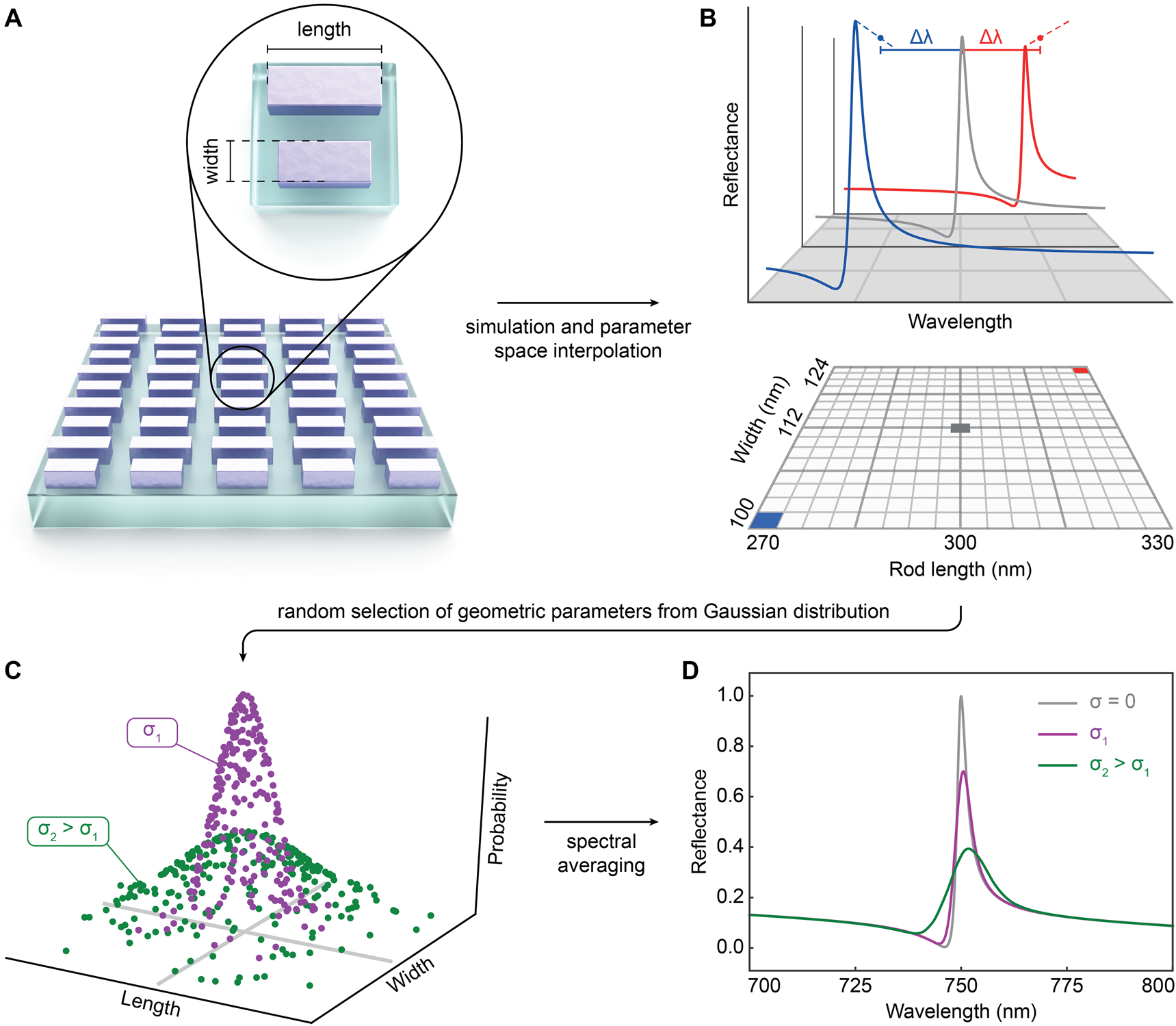
Numerical modelling of resonance broadening. (A) Sketch of a BIC unit cell design and identification of two geometric parameters with strong influence on the resonance. (B) A 5 by 5 grid of simulation points with variation of the parameters by ±7.5% and ±15% is interpolated in 1000 steps, resulting in a finely gridded parameter space of geometric variation. (C) Selection of points out of Gaussian random distribution for two different standard deviations σ 1 and σ 2 > σ 1. (D) Spectral averaging yields a broadened resonance spectrum corresponding to a fabricated metasurface with random geometric variation.
One straightforward way of modelling the fabrication-induced effects on the optical response of the metasurface is to introduce random geometrical variations for each unit cell independently. However, this approach would lead to a prohibitively large simulation domain for common metasurface arrangements, which often require more than 100 unit cells to support their respective resonant modes [10, 21]. Instead, our methodology simulates the spectra of full unit cell arrays with varying geometrical parameters and uses statistical averaging to predict the final optical response of the fabricated metasurfaces. In order to implement this method numerically, the two chosen geometric parameters are varied by ±7.5% and ±15%, respectively, to construct a 5 by 5 grid of equidistant points, where the initial parameter values of the design are located at the center (Figure 1B), drastically reducing the simulation overhead. Reflectance spectra for all 25 parameter combinations are then numerically simulated and linearly interpolated using n = 1000 steps. This process creates a parameter space with a fine grid of simulated spectra, allowing us to capture even small variations of the geometric parameters. To model the geometric variations in a fabricated sample, N = 5000 random points are selected from a Gaussian random distribution over the parameter space, mimicking the experimental distribution of slightly different geometrical parameters (Figure 1C). The spectra corresponding to the randomly drawn points of the parameter space are the naveraged to obtain an approximation of the optical response of a fabricated metasurface (Figure 1D).
Notably, even low standard deviations as low as σ = 1 nm or σ = 3 nm can have a strong influence on the resonance amplitude and the Q-factor. For example, the resonance amplitude of the ellipse design for σ = 1 nm is at around 0.8, whereas it is at 0.7 for the rods, illustrating the markedly different impact of the same amount of fabrication tolerance on BIC unit cell designs with the same resonance position and Q-factor (Figure 2A–C). This behavior clearly shows that the magnitude of resonance broadening is correlated with each individual unit cell design. Figure 2D displays the Q-factor of the different BIC designs for standard deviations of the geometrical variation ranging from σ = 0 nm to σ = 5 nm. Notably, the ellipse design retains the highest Q-factor over the entire variation range, while the other designs fall off more quickly (Figure 2D). Fitting an inverse quadratic function to the Q-factors shows good agreement and confirms the proportionality of Q(σ) ∼ 1/σ 2 previously found for photonic crystal cavities [34]. Interestingly, the ordering of the different designs by their Q-factors is maintained for all standard deviations as well, highlighting that the fabrication robustness is an underlying property of each BIC design.
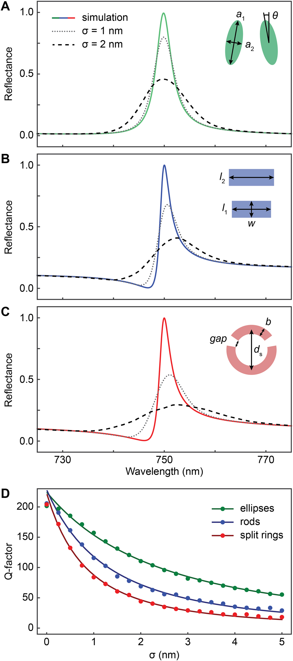
Broadening model predictions for common BIC geometries.
(A–C) Simulated quasi-BIC resonance spectra and modelled spectra for the different resonator designs and two standard deviation values for the geometric variation. For σ = 3 nm both the resonance intensity and the Q-factor are significantly reduced compared to the simulation. (D) Calculated Q-factor against standard deviation values of the geometrical parameters up to σ = 5 nm (points). Inverse quadratic fits (lines) showing good agreement with the Q-factors of the broadened resonances. The tilted ellipse design exhibits higher resonance sharpness over the entire variation range compared to the other designs.
The three BIC metasurface geometries are then realized experimentally in amorphous silicon through electron-beam lithography and directional reactive ion etching (for details see Section 4). To quantify the fabrication tolerance experimentally, we capture large sets of scanning electron microscopy (SEM) images for each BIC unit cell design and perform image processing to assess the distribution of the geometric parameters. Specifically, in order to achieve a high level of uniformity and reproducibility for the parameter extraction, we implement an image fitting algorithm to overlap the designs with the SEM images. Images are first up-scaled eightfold for higher precision and undergo a multistep denoising process through applying a series of filters (Figure 3, top). First, a bilateral filter removes fine noise from the image while preserving the edges of larger objects. The next step is a set of erosion and dilation filters, resulting in overall brighter and smoother features in the images, bringing out the resonator geometry in more detail. Subsequently, a threshold is applied to transform the image into filled black and white image areas. Finally, the design can be fitted iteratively by creating a mask with varying geometrical parameters and maximizing the number of overlapping pixels between mask and image to obtain the optimal parameter values. For better statistics, this fitting algorithm is applied to 10 images containing 12 unit cells for each design, providing higher accuracy as well as consistency and reproducibility compared to a manual measurement of the parameters from the SEM images. The resulting distributions of extracted geometric parameters clearly show Gaussian profiles for all unit cell designs, confirming the assumption of the theoretical model (Figure 4).
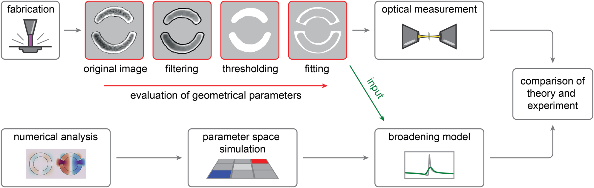
Methodology for comparison of theory and experimental realization. Evaluation of fabricated metasurface geometric parameters by fitting of resonator designs, which are used as input for the broadening model to calculate a resonance that mimics random fluctuations in a fabricated sample. The modelled resonance is compared to the measured spectra of the fabricated metasurface.
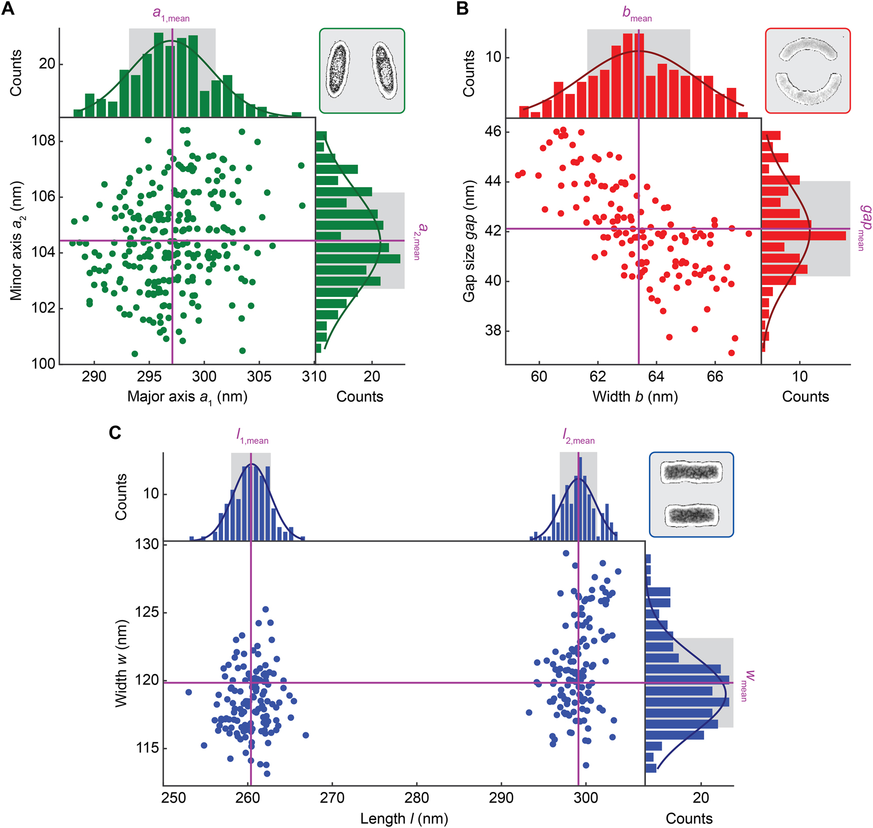
Evaluation of fabrication-induced variation of resonator geometry.
Structural analysis output of resonator dimensions for the tilted ellipse (A), split ring (B) and double rod (C) unit cell designs, all of which show a Gaussian distribution of their geometric parameters.
Comparing the mean dimensions from the fabricated structures to the design values (Figure S1, Supplementary material), only the asymmetric rod design shows a notable discrepancy from the as-designed geometry with a 12 nm difference in rod width (Figure 4C), with all other designs closer to the desired parameters. Since the metasurface arrays for all three BIC unit cell designs are fabricated on one substrate, we average the standard deviations of all designs to obtain a unified measure of the geometric tolerances in fabrication, which yields σ avg = 2.4 nm. However, it is important to note that if metasurfaces from different fabrication runs are to be compared, the standard deviation of each sample should be determined separately. Interestingly, in the split ring design, the fitted parameters show a correlation between gap size and width, where overall up- and downscaled structures are more common. This effect is absent in the other BIC designs due to a simpler unit cell structure of two resonator elements with larger spatial separation.
The average geometric variation σ avg determined from the SEM images is used as an input for our numerical broadening model (Figure 3, bottom), allowing us to predict realistic BIC resonance properties from first-principle electromagnetic simulations. In order to improve the accuracy of the prediction, we take into account some intrinsic sources of error related to the SEM imaging. For example, the imaging quality is affected by a small amount of lens aberration, which leads to a magnification of objects at the image corners and thus to an increased observed size, while objects in the center remain almost unchanged. In turn, this increases the standard deviation of geometrical parameters independent of the actual variation of the fabricated metasurface, since slight blurring at the edge of objects can already influence the extracted parameter on the order of a few nanometers. Furthermore, because the SEM images are taken at a resolution of 2048 by 1536 pixels and one pixel corresponds to around 1 nm at 60,000× magnification, there is a natural limit to the accuracy of this methodology, which we estimate at σ im = 1 nm. Electrostatic charging of the metasurface during imaging can similarly lead to slight variations of the exposure between different images taken for the same BIC design. To quantify this effect, we calculate the standard deviation of the mean geometrical parameters between different images and obtain a correction factor of σ c = 0.5 nm. These considerations are important so that the true fabrication tolerance is not overestimated, which would lead to a very broad resonance (see Figure 2A–C for σ = 3 nm).
Combining these effects, we obtain a total standard deviation of σ tot = σ avg − σ im − σ c = 0.9 nm. The modelled resonances with this standard deviation value show a reduction in Q-factor of around 40–110 compared to the as-designed value of Q = 200 for all investigated unit cell geometries (Figure 5A), highlighting the crucial importance of taking these broadening effects into account. Significantly, the tilted ellipse design stands out as the BIC unit cell that retains the highest Q-factor, while the other designs have broader resonances and thus lower Q-factors. In experimental transmission measurements (Figure 5B, for details see Section 4), both the resonance shapes and amplitudes are in excellent agreement with the predictions of our broadening model apart from a slightly lower resonance wavelength. This offset is most likely related to a small discrepancy between the dielectric function of silicon as used in the simulations and the actual optical properties of the thin film as deposited in experiments. Nevertheless, the resonance Q-factors of the fabricated metasurfaces and our model show good agreement and demonstrate the possibility to assess the influence of random geometric variation during fabrication on the resonance, enabling the accelerated discovery, and development of robust BIC-based nanophotonic systems.
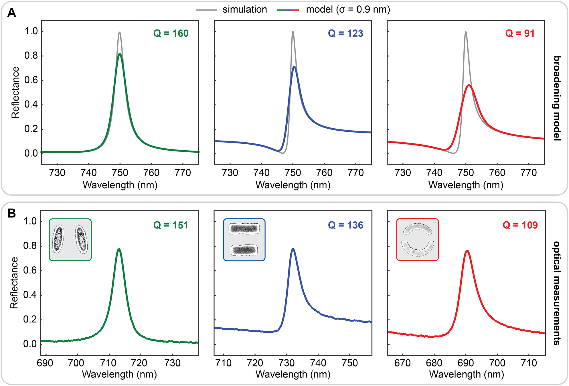
Comparison between broadening model output and measured optical response of the BIC metasurfaces.
(A) Modelled BIC resonance spectra for the standard deviation value of geometric variation derived from SEM image analysis. (B) Measured spectra of the fabricated metasurfaces showing excellent agreement with the model.
3 Conclusion
In conclusion, we have developed a method for modelling the effects of unavoidable fabrication tolerances on the optical performance of BIC-based metasurfaces. For each given unit cell design, our methodology first maps the parameter space of fabrication-induced geometrical variations using numerical simulations of the metasurface reflectance. Subsequently, a statistical approach is used to predict the modified reflectance response as a function of the standard deviation of the geometrical parameters. Comparing three prominent designs (tilted ellipses, asymmetric double rods, and split rings), we find a strong disparity in fabrication robustness behavior, with the tilted ellipse design showing more than 50% higher Q-factors compared to the split rings, demonstrating the crucial impact of such geometrical broadening effects. The numerical predictions provide important guidelines for the design of BIC-based unit cells and are in excellent agreement with optical measurements on fabricated metasurface samples, where the experimental variation of the geometrical parameters is extracted using sophisticated analysis of sets of SEM images. Since our methodology only requires simulated optical spectra as input, it is not limited to BIC-driven geometries, but can be applied to all nanophotonic systems where high Q-factors are needed for critical applications, enabling the a-priori design and discovery of new classes of fabrication-robust resonant systems in fields ranging from biomolecular sensing and environmental monitoring to tailored light/matter interaction.
4 Methods
Numerical simulations: Simulated reflectance spectra of the different metasurface designs were obtained using the finite-element frequency-domain Maxwell solver included in CST Studio Suite 2020 (Dassault Systèmes), with periodic boundary conditions applied at both sides of the unit cell.
Metasurface fabrication: The all-dielectric resonator geometries were fabricated from a 100 nm thick layer of amorphous silicon deposited onto a fused silica substrate by plasma-enhanced chemical vapor deposition (PECVD). For the lithography step, the sample was first spin-coated with a layer of PMMA 950K A2 photoresist followed by a highly conducting polymer layer (ESpacer 300Z) to avoid charging effects during exposure. Subsequently, the three BIC unit cell designs were patterned using electron-beam lithography (Raith eLINE Plus) with an acceleration voltage of 20 kV and a 7.5 μm aperture. After development for 50 s in 3:1 MIBK:IPA solution, a hard-mask consisting of 14 nm SiO2 and 20 nm Cr was deposited by evaporation, followed by lift-off in Microposit Remover 1165 for 2 h at 80° C. The pattern was then transferred into the silicon layer by reactive ion etching (RIE). Lastly, the chrome layer was removed by wet etching and the SiO2 layer with an additional RIE step. The obtained Si resonator metasurfaces on a silica substrate were then imaged for geometrical analysis using the same Raith eLINE Plus system.
Optical measurement: The spectral characterization of the fabricated metasurface samples was carried out with a WiTec optical microscope in transmission mode using a collimated Thorlabs OSL2 white light source for illumination. The light is collected with an Olympus 10× objective (NA = 0.25), normalized to a background spectrum on the sample and converted to reflectance by 1 − transmittance.
SEM image fitting and geometrical analysis: For evaluation of the SEM images and the dimensions of the unit cells, a Python script was written based on the OpenCV library for computer vision. In order to detect individual resonators, the input image was filtered, starting with a bilateral filter for noise reduction followed by a set of dilation and erosion filters. This series of filters allows for thresholding of the image to isolate the features from noise and facilitate corner recognition, which is needed to get the resonators position in the image as well as its size to function as starting parameters for the geometry fitting. For this process, a mask of the target resonator was generated, placed on top of the processed resonator image, and the overlapped area calculated by counting the overlapping pixels, the number of which was then returned to the optimizer. Finally, the fit parameters were converted from pixels to nanometers by reading out the length of the scale bar in the SEM image.
Funding source: Deutsche Forschungsgemeinschaft doi.org/10.13039/501100001659
Award Identifier / Grant number: EXC 2089/1-390776260
Funding source: Emmy Noether Program TI 1063/1
Funding source: Engineering and Physical Sciences Research Council doi.org/10.13039/501100000266
Award Identifier / Grant number: EP/P033369/1
-
Author contributions: All the authors have accepted responsibility for the entire content of this submitted manuscript and approved submission.
-
Research funding: This work was funded by the Deutsche Forschungsgemeinschaft (DFG, German Research Foundation) under Germany’s Excellence Strategy – EXC 2089/1-390776260 and the Emmy Noether Program TI 1063/1. The authors acknowledge support from the Bavarian program Solar Energies Go Hybrid (SolTech) and the Center for NanoScience (CeNS). S. A. M. additionally acknowledges the EPSRC (EP/P033369/1) and the Lee-Lucas Chair in Physics.
-
Conflict of interest statement: The authors declare no conflicts of interest regarding this article.
References
[1] A. F. Koenderink, A. Alù, and A. Polman, “Nanophotonics: shrinking light-based technology,” Science, vol. 348, pp. 516–521, 2015, https://doi.org/10.1126/science.1261243.Suche in Google Scholar PubMed
[2] D. K. Gramotnev and S. I. Bozhevolnyi, “Plasmonics beyond the diffraction limit,” Nat. Photonics, vol. 4, pp. 83–91, 2010, https://doi.org/10.1038/nphoton.2009.282.Suche in Google Scholar
[3] G. Baffou and R. Quidant, “Nanoplasmonics for chemistry,” Chem. Soc. Rev., vol. 43, pp. 3898–3907, 2014, https://doi.org/10.1039/c3cs60364d.Suche in Google Scholar PubMed
[4] J. Dorfmüller, R. Vogelgesang, W. Khunsin, C. Rockstuhl, C. Etrich, and K. Kern, “Plasmonic nanowire antennas: experiment, simulation, and theory,” Nano Lett., vol. 10, pp. 3596–3603, 2010, https://doi.org/10.1021/nl101921y.Suche in Google Scholar PubMed
[5] D. G. Baranov, D. A. Zuev, S. I. Lepeshov, et al.., “All-dielectric nanophotonics: the quest for better materials and fabrication techniques,” Optica, vol. 4, p. 814, 2017, https://doi.org/10.1364/optica.4.000814.Suche in Google Scholar
[6] K. Koshelev and Y. Kivshar, “Dielectric resonant metaphotonics,” ACS Photonics, vol. 8, pp. 102–112, 2020, https://doi.org/10.1021/acsphotonics.0c01315.Suche in Google Scholar
[7] I. Sinev, F. Komissarenko, I. Iorsh, D. Permyakov, A. Samusev, and A. Bogdanov, “Steering of guided light with dielectric nanoantennas,” ACS Photonics, vol. 7, pp. 680–686, 2020, https://doi.org/10.1021/acsphotonics.9b01515.Suche in Google Scholar
[8] R. Alaee, M. Albooyeh, A. Rahimzadegan, M. S. Mirmoosa, Y. S. Kivshar, and C. Rockstuhl, “All-dielectric reciprocal bianisotropic nanoparticles,” Phys. Rev. B, vol. 92, p. 245130, 2015, https://doi.org/10.1103/physrevb.92.245130.Suche in Google Scholar
[9] L. Hüttenhofer, A. Tittl, L. Kühner, E. Cortés, and S. A. Maier, “Anapole-assisted absorption engineering in arrays of coupled amorphous gallium phosphide nanodisks,” ACS Photonics, vol. 8, pp. 1469–1476, 2021, https://doi.org/10.1021/acsphotonics.1c00238.Suche in Google Scholar
[10] Y. Yang, I. I. Kravchenko, D. P. Briggs, and J. Valentine, “All-dielectric metasurface analogue of electromagnetically induced transparency,” Nat. Commun., vol. 5, p. 5753, 2014, https://doi.org/10.1038/ncomms6753.Suche in Google Scholar PubMed
[11] G. Zograf, K. Baryshnikova, M. Petrov, and S. Makarov, “Enhanced Raman scattering for probing NearField distribution in AllDielectric nanostructures,” Adv. Photonics Res., vol. 2, p. 2000139, 2021, https://doi.org/10.1002/adpr.202000139.Suche in Google Scholar
[12] C. W. Hsu, B. Zhen, A. D. Stone, J. D. Joannopoulos, and M. Soljačić, “Bound states in the continuum,” Nat. Rev. Mater., vol. 1, p. 16048, 2016, https://doi.org/10.1038/natrevmats.2016.48.Suche in Google Scholar
[13] K. Koshelev, G. Favraud, A. Bogdanov, Y. Kivshar, and A. Fratalocchi, “Nonradiating photonics with resonant dielectric nanostructures,” Nanophotonics-Berlin, vol. 8, pp. 725–745, 2019, https://doi.org/10.1515/nanoph-2019-0024.Suche in Google Scholar
[14] M. V. Rybin, K. L. Koshelev, Z. F. Sadrieva, et al.., “High-Q supercavity modes in subwavelength dielectric resonators,” Phys. Rev. Lett., vol. 119, p. 243901, 2017, https://doi.org/10.1103/physrevlett.119.243901.Suche in Google Scholar
[15] Z. Sadrieva, K. Frizyuk, M. Petrov, Y. Kivshar, and A. Bogdanov, “Multipolar origin of bound states in the continuum,” Phys. Rev. B, vol. 100, p. 115303, 2019, https://doi.org/10.1103/physrevb.100.115303.Suche in Google Scholar
[16] S. Li, C. Zhou, T. Liu, and S. Xiao, “Symmetry-protected bound states in the continuum supported by all-dielectric metasurfaces,” Phys. Rev. A, vol. 100, p. 063803, 2019, https://doi.org/10.1103/physreva.100.063803.Suche in Google Scholar
[17] K. Koshelev, S. Lepeshov, M. Liu, A. Bogdanov, and Y. Kivshar, “Asymmetric metasurfaces with high-Q resonances governed by bound states in the continuum,” Phys. Rev. Lett., vol. 121, p. 193903, 2018, https://doi.org/10.1103/physrevlett.121.193903.Suche in Google Scholar
[18] S. I. Azzam and A. V. Kildishev, “Photonic bound states in the continuum: from basics to applications,” Adv. Opt. Mater., vol. 9, p. 2001469, 2021, https://doi.org/10.1002/adom.202001469.Suche in Google Scholar
[19] O. Yavas, M. Svedendahl, P. Dobosz, V. Sanz, and R. Quidant, “On-a-chip biosensing based on all-dielectric nanoresonators,” Nano Lett., vol. 17, pp. 4421–4426, 2017, https://doi.org/10.1021/acs.nanolett.7b01518.Suche in Google Scholar PubMed
[20] A. Tittl, A. JohnHerpin, A. Leitis, E. R. Arvelo, and H. Altug, “Metasurface based molecular biosensing aided by artificial intelligence,” Angew. Chem. Int. Ed., vol. 58, pp. 14810–14822, 2019, https://doi.org/10.1002/anie.201901443.Suche in Google Scholar PubMed
[21] F. Yesilkoy, E. R. Arvelo, Y. Jahani, et al.., “Ultrasensitive hyperspectral imaging and biodetection enabled by dielectric metasurfaces,” Nat. Photonics, vol. 13, pp. 390–396, 2019, https://doi.org/10.1038/s41566-019-0394-6.Suche in Google Scholar
[22] S. Romano, M. Mangini, E. Penzo, et al.., “Ultrasensitive surface refractive index imaging based on quasi-bound states in the continuum,” ACS Nano, vol. 14, pp. 15417–15427, 2020, https://doi.org/10.1021/acsnano.0c06050.Suche in Google Scholar PubMed
[23] D. N. Maksimov, V. S. Gerasimov, S. Romano, and S. P. Polyutov, “Refractive index sensing with optical bound states in the continuum,” Opt. Express, vol. 28, p. 38907, 2020, https://doi.org/10.1364/oe.411749.Suche in Google Scholar PubMed
[24] A. Tittl, A. Leitis, M. Liu, et al.., “Imaging-based molecular barcoding with pixelated dielectric metasurfaces,” Science, vol. 360, pp. 1105–1109, 2018, https://doi.org/10.1126/science.aas9768.Suche in Google Scholar PubMed
[25] K. Koshelev, S. Kruk, E. Melik-Gaykazyan, et al.., “Subwavelength dielectric resonators for nonlinear nanophotonics,” Science, vol. 367, pp. 288–292, 2020, https://doi.org/10.1126/science.aaz3985.Suche in Google Scholar PubMed
[26] N. Bernhardt, K. Koshelev, S. J. U. White, et al.., “Quasi-BIC resonant enhancement of second-harmonic generation in WS2 monolayers,” Nano Lett., vol. 20, pp. 5309–5314, 2020, https://doi.org/10.1021/acs.nanolett.0c01603.Suche in Google Scholar PubMed
[27] S. Busschaert, R. Reimann, M. Cavigelli, R. Khelifa, A. Jain, and L. Novotny, “Transition metal dichalcogenide resonators for second harmonic signal enhancement,” ACS Photonics, vol. 7, pp. 2482–2488, 2020, https://doi.org/10.1021/acsphotonics.0c00751.Suche in Google Scholar
[28] A. Kodigala, T. Lepetit, Q. Gu, B. Bahari, Y. Fainman, and B. Kanté, “Lasing action from photonic bound states in continuum,” Nature, vol. 541, pp. 196–199, 2017, https://doi.org/10.1038/nature20799.Suche in Google Scholar PubMed
[29] L. Ni, Z. Wang, C. Peng, and Z. Li, “Tunable optical bound states in the continuum beyond in-plane symmetry protection,” Phys. Rev. B, vol. 94, p. 245148, 2016, https://doi.org/10.1103/physrevb.94.245148.Suche in Google Scholar
[30] J. F. Algorri, D. C. Zografopoulos, A. Ferraro, B. García-Cámara, R. Beccherelli, and J. M. Sánchez-Pena, “Ultrahigh-quality factor resonant dielectric metasurfaces based on hollow nanocuboids,” Opt. Express, vol. 27, p. 6320, 2019, https://doi.org/10.1364/oe.27.006320.Suche in Google Scholar PubMed
[31] M. Soler, A. Scholtz, R. Zeto, and A. M. Armani, “Engineering photonics solutions for COVID-19,” APL Photonics, vol. 5, p. 090901, 2020, https://doi.org/10.1063/5.0021270.Suche in Google Scholar PubMed PubMed Central
[32] B. Chocarro-Ruiz, A. Fernández-Gavela, S. Herranz, and L. M. Lechuga, “Nanophotonic label-free biosensors for environmental monitoring,” Curr. Opin. Biotechnol., vol. 45, pp. 175–183, 2017, https://doi.org/10.1016/j.copbio.2017.03.016.Suche in Google Scholar PubMed
[33] M. Liu and D.-Y. Choi, “Extreme huygens’ metasurfaces based on quasi-bound states in the continuum,” Nano Lett., vol. 18, pp. 8062–8069, 2018, https://doi.org/10.1021/acs.nanolett.8b04774.Suche in Google Scholar PubMed
[34] H. Friedrich and D. Wintgen, “Interfering resonances and bound states in the continuum,” Phys. Rev. A, vol. 32, pp. 3231–3242, 1985, https://doi.org/10.1103/physreva.32.3231.Suche in Google Scholar PubMed
Supplementary Material
The online version of this article offers supplementary material (https://doi.org/10.1515/nanoph-2021-0391).
© 2021 Julius Kühne et al., published by De Gruyter, Berlin/Boston
This work is licensed under the Creative Commons Attribution 4.0 International License.
Artikel in diesem Heft
- Frontmatter
- Editorial
- The science of harnessing light’s darkness
- Reviews
- Bound states in the continuum in resonant nanostructures: an overview of engineered materials for tailored applications
- Reconfigurable nonlinear response of dielectric and semiconductor metasurfaces
- Research Articles
- Active angular tuning and switching of Brewster quasi bound states in the continuum in magneto-optic metasurfaces
- Resonance-forbidden second-harmonic generation in nonlinear photonic crystals
- Dispersive bands of bound states in the continuum
- Dressed emitters as impurities
- Engineering gallium phosphide nanostructures for efficient nonlinear photonics and enhanced spectroscopies
- Ultraviolet second harmonic generation from Mie-resonant lithium niobate nanospheres
- Label-free DNA biosensing by topological light confinement
- Guided-mode resonance on pedestal and half-buried high-contrast gratings for biosensing applications
- Ways to achieve efficient non-local vortex beam generation
- Fabrication robustness in BIC metasurfaces
- Bound states in the continuum in periodic structures with structural disorder
- Demonstration of on-chip gigahertz acousto-optic modulation at near-visible wavelengths
- Integrated diffraction gratings on the Bloch surface wave platform supporting bound states in the continuum
- Ultrahigh-Q system of a few coaxial disks
- Bound states in the continuum in strong-coupling and weak-coupling regimes under the cylinder – ring transition
- Two tractable models of dynamic light scattering and their application to Fano resonances
- Polarization-independent anapole response of a trimer-based dielectric metasurface
- Transparent hybrid anapole metasurfaces with negligible electromagnetic coupling for phase engineering
- Nonradiating sources for efficient wireless power transfer
- Anapole-enabled RFID security against far-field attacks