Integrated diffraction gratings on the Bloch surface wave platform supporting bound states in the continuum
-
Evgeni A. Bezus
 ,
Dmitry A. Bykov
and
Leonid L. Doskolovich
,
Dmitry A. Bykov
and
Leonid L. Doskolovich


Abstract
We propose and theoretically and numerically investigate integrated diffraction gratings for the Bloch surface wave (BSW) platform, which have subwavelength or near-subwavelength period. We demonstrate that, in the oblique incidence geometry of a transverse-electric polarized BSW and with a properly chosen band gap configuration of the photonic crystal supporting the surface waves, the proposed structures operate in the scattering-free regime, when the energy of the incident BSW is divided between the reflected and transmitted BSWs with the same polarization corresponding to the propagating diffraction orders of the grating, and not scattered away from the propagation surface. In this regime, the studied integrated gratings support high-Q resonances and bound states in the continuum not only in the subwavelength case when only the specular (zeroth) diffraction orders propagate, but also in the case when non-evanescent zeroth and −1st diffraction orders satisfy the so-called Littrow mounting condition. The proposed integrated gratings on the BSW platform can be used as efficient narrowband spatial or spectral filters operating in reflection, or as BSW beam splitters or deflectors operating in transmission. The obtained results may find application in two-dimensional photonic circuits for steering the BSW propagation.
1 Introduction
Resonant effects play a crucial role in photonics, since they enable creating photonic structures with unique optical properties that can be used in sophisticated devices for optical filtering, sensing and switching, among other applications [1]. In recent decade, a special kind of resonant optical states has attracted considerable research attention, namely, the so-called bound states in the continuum (BICs) also referred to as embedded eigenstates. The BIC phenomenon was first theoretically discovered almost a century ago by von Neumann and Wigner for an electronic system with an artificially constructed potential [2]. In photonics, BICs are “non-radiative” eigenmodes (i.e., eigenmodes with a real frequency and, hence, an infinite lifetime) supported by optical structures with open scattering channels [3–6]. The scattering of the BIC energy to the open channels is prevented either due to symmetry incompatibility [7], or due to interference effects caused by the interaction of several resonators [8] or of several modes in the same resonator [9]. Along with the fundamental importance, BICs are of great practical interest, since in real photonic structures, due to finiteness, fabrication imperfections, and material absorption, the BICs collapse to resonances with finite, but potentially very high quality factor (often referred to as quasi-BICs) useful for numerous applications.
One of the most widely known and extensively studied classes of resonant photonic structures supporting bound states in the continuum is constituted by periodic structures such as photonic crystal slabs [10–14], guided-mode resonant gratings [15–17], or periodic arrays of dielectric rods or spheres [18–20]. In these structures, the open scattering channels correspond to the free-space diffraction orders. Taking into account the development of “two-dimensional” optics on several integrated platforms [21–25], bringing the concept of resonant diffraction gratings (including the gratings supporting BICs) to the on-chip geometry, in which the incident wave and the scattering channels, i.e., the reflected and transmitted diffraction orders correspond not to free-space waves but to modes of a certain waveguide, is of great interest. In our previous works, we proposed and studied integrated analogues of high-contrast gratings for surface plasmon polaritons (SPPs) [26, 27]. Although these structures were shown to be able to resonantly reflect the incident SPPs in a narrow or wide spectral range, the BICs (or quasi-BICs) in such “on-chip” gratings were not explicitly studied. To the best of our knowledge, the only study of quasi-BICs in an integrated grating (on a silicon waveguide platform, where the incident wave and the diffraction orders were the modes of a silicon slab waveguide) was presented in a recent paper [28].
In the present work, we propose and study integrated diffraction gratings for the Bloch surface wave (BSW) platform. Bloch surface waves are surface electromagnetic waves supported by the interfaces of photonic crystals (in the simplest case, one-dimensional) [25, 29]. Due to the fact that they can be supported by all-dielectric structures, BSWs are considered a promising alternative to surface plasmon polaritons in optical sensing applications [30–32] and for creating flat (“two-dimensional”) photonic circuits [25]. Previously proposed two-dimensional optical elements for BSWs include on-chip prisms [33], lenses [25, 34, 35], Bragg gratings [36] and their phase-shifted counterparts [37, 38], and large-period diffraction gratings operating in the “scalar diffraction” regime [33]. In all these works, the incident waves were the transverse-electric (TE-) polarized Bloch surface waves supported by interfaces of one-dimensional dielectric photonic crystals.
Integrated gratings studied in this work have subwavelength or near-wavelength periods and consist of periodically arranged dielectric pillars on the surface of an all-dielectric one-dimensional photonic crystal. We theoretically and numerically demonstrate that such structures can support “true” (i.e., not quasi-) bound states in the continuum if an additional “non-radiative” condition is fulfilled. This condition, which can also be referred to as the scattering-free condition, requires the absence of the “parasitic” scattering of the incident BSW away from the propagation interface upon diffraction by the integrated grating. We show that this condition can be satisfied in the oblique incidence geometry by tailoring the band gap configuration of the photonic crystal. We consider two regimes, in which this condition can be implemented at realistic parameters: (1) the subwavelength regime, in which only the zeroth reflected and transmitted diffraction orders propagate, and (2) the regime, when the −1st reflected and transmitted orders are also supported by the grating. We demonstrate that the integrated gratings exhibit BICs not only in the first (subwavelength) regime, but also in the second regime, provided that the so-called Littrow mounting condition is fulfilled. The proposed structures may find application as efficient narrowband reflectors (filters) as well as beam splitters and deflectors for Bloch surface waves.
2 Integrated diffraction gratings on the BSW platform and parasitic scattering suppression
The geometry of the proposed structure is shown in Figure 1. The integrated grating consists of a periodic set (with period d) of dielectric pillars with rectangular cross-section, height h, transverse size (width) w, and longitudinal size (length) l located on the surface of a one-dimensional dielectric photonic crystal (PhC). The PhC period consists of two layers with refractive indices n
1 and n
2 and thicknesses h
1 and h
2. In the present work, for the sake of simplicity, we assume that the dielectric pillars constituting the grating are made of the same material as the upper layer of the photonic crystal having the refractive index n
1. The refractive index of the superstrate equals n
0. In order to tune the parameters of the BSW supported by the PhC interface, the thickness of the upper layer of the PhC differs from the “usual” one (h
1) and equals
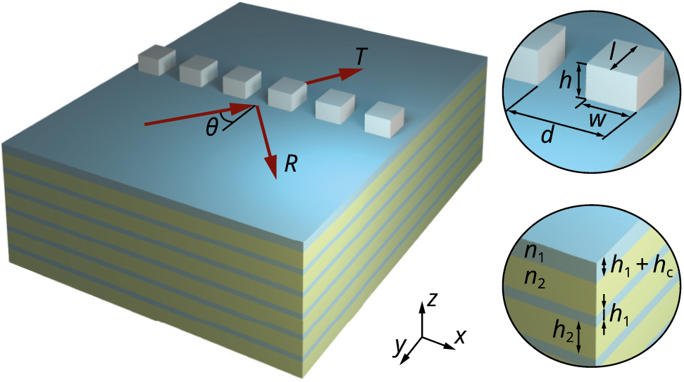
Geometry of the investigated integrated gratings for Bloch surface waves supported by the interface of a one-dimensional photonic crystal.
In what follows, we consider the case when the wave incident on the integrated grating is a TE-polarized Bloch surface wave propagating along the PhC interface. Such a BSW satisfies the following dispersion relation [39]:
where
In the general case of oblique incidence of a BSW on an integrated grating (see Figure 1), the incident surface wave has the in-plane wavevector components k x,0 = k BSW sin θ and k y,0 = k BSW cos θ, where θ is the angle of incidence, which is assumed to be positive in the rest of the paper. Due to periodicity, the grating generates a set of reflected and transmitted diffraction orders with the following x-components of the wavevector [40]:
In the case of a conventional (non-integrated) diffraction grating operating in non-conical (planar) mounting, each of the diffraction orders corresponds to either a propagating or an evanescent plane wave having the same polarization as the incident wave [41]. With integrated gratings operating with guided modes or surface electromagnetic waves, the situation is much more sophisticated. Due to the fact that the structure is not invariant to translation in the direction of the z axis, each of the diffraction orders will, in the most general case, “contain” not only a reflected or transmitted BSW having the same polarization as the incident one (TE-polarization for all the examples considered below), but also a “cross-polarized” (TM-polarized) BSW as well as non-guided radiation scattered out of the propagation surface to the superstrate (plane waves in a homogeneous dielectric with the refractive index n 0) and to the substrate (“bulk” modes of a one-dimensional photonic crystal). As in the case of the on-chip optical elements for surface plasmon polaritons [26, 27, 42, 43], these “parasitic” waves may critically hinder the performance of the integrated optical elements for BSWs and, in particular, make it impossible to achieve high-Q resonant states.
However, let us show that by tailoring the configuration of the bandgaps of the photonic crystal and by choosing the incidence angle of the BSW impinging on the grating, one can completely eliminate the parasitic scattering and polarization conversion losses, i.e., satisfy the “non-radiative” or “scattering-free” condition mentioned above. For now, let us assume that the integrated grating is subwavelength, i.e., that only the zeroth reflected and transmitted diffraction orders having the x wavevector component equal to the wavevector component of the incident wave k
x,0 = k
0
n
eff,TE sin θ are propagating. In this case, total suppression of the “parasitic” waves is possible if the following conditions are fulfilled. First, the photonic crystal must have a continuous bandgap for both TE- and TM-polarized waves with the in-plane wavevector components
Indeed, in this case, the x wavevector component of the incident BSW, which is conserved for the zeroth reflected and transmitted diffraction orders, exceeds the magnitude of the wavevector of the plane waves in the superstrate, as well as of the TM-polarized BSWs. This means that these waves are evanescent and do not carry energy. In addition, due to the bandgap configuration, such k x,0 values correspond to evanescent “bulk” modes of the photonic crystal. Therefore, according to Eqs. (2) and (3), at angles of incidence
the energy of the incident TE-polarized BSW is divided only between the reflected and transmitted TE-polarized BSWs corresponding to the zeroth diffraction orders. A more detailed description of this mechanism (in particular, regarding the cancellation of scattering into the “bulk” modes of the photonic crystal) is presented in the supplementary material. In Subsection 3.1, we provide the results of rigorous numerical simulations, which confirm the presented theoretical reasoning.
Note that a similar approach for suppressing unwanted scattering was recently proposed for the dielectric slab waveguide platform [44, 45] and utilized in our previous works for designing simple ridge- and groove-based structures supporting high-Q resonances [46] and bound states in the continuum [47, 48]. Let us also note that by satisfying additional conditions, it is also possible to suppress the parasitic scattering in the non-subwavelength regime. We will discuss this case in Subsection 3.2.
3 Optical properties of the integrated gratings for BSWs
In this section, we demonstrate that integrated diffraction gratings for BSWs satisfying the “scattering-free” conditions described above exhibit remarkable optical properties, in particular, high-Q resonances and bound states in the continuum. In what follows, we consider an example with the following parameters: central free-space wavelength λ = 630 nm, refractive indices of the materials n
0 = 1, n
1 = 3.3212 (GaP) [49, 50], and n
2 = 1.4762 (SiO2) [50, 51], thicknesses of the photonic crystal layers h
1 = 0.04λ = 25 nm and h
2 = 0.26λ = 164 nm, thickness of the upper layer of the photonic crystal
Before moving further, we would like to stress that the chosen parameters are not unique, and that the results similar to the ones presented below can be obtained for a wide range of materials and wavelengths, provided that the geometrical parameters of the PhC layers and the angle of incidence of the BSW impinging on the grating are chosen in a proper way ensuring the “scattering-free” regime described by Eq. (4).
All the simulation results presented below were obtained using an in-house implementation of the three-dimensional Fourier modal method (FMM; also known as rigorous coupled-wave analysis) [41, 52, 53] adapted for the solution of the integrated optics problems [54, 55] and enabling the calculation of the eigenmodes of the investigated periodic photonic structures [56]. For the details on the simulation of integrated diffraction gratings for surface electromagnetic waves, we refer the reader to our previous work [26], where on-chip plasmonic gratings were studied.
The rest of this section is organized as follows. In Subsection 3.1, we consider integrated gratings operating in the so-called subwavelength regime, in which only the zeroth diffraction orders propagate. In Subsection 3.2, we study non-subwavelength gratings, focusing on a particular case when the grating supports zeroth and −1st diffraction orders, and the propagation directions of the incident wave and the −1st reflected order are exactly opposite (the so-called Littrow mounting).
3.1 Subwavelength gratings
Let us start by studying subwavelength integrated gratings, in which only the zeroth reflected and transmitted diffraction orders are non-evanescent, i.e., the following inequalities hold: |k x,1| = |k x,0 + 2π/d| > k 0 n eff,TE, |k x,−1| = |k x,0 − 2π/d| > k 0 n eff,TE. Let us choose a fixed angle of incidence θ = 55°, which exceeds the critical angle θ cr given by Eq. (4). For this angle of incidence and the chosen parameters of the example, the inequalities ensuring the subwavelength regime hold at grating periods d < λ/4.366. Figure 2a shows the reflectance R 0 (diffraction efficiency of the zeroth reflected order) of a grating with the pillar height h = 33 nm and fill factor w/d = 0.5 versus the wavelength λ and grating length l normalized by the grating period d. Such a parameter space proved convenient for the investigation of both the conventional (non-integrated) [57] and on-chip [26, 27] diffraction gratings. Let us note that in terms of this parameter space, the length l of an integrated grating is equivalent to the thickness (height) of a conventional grating operating with the free-space radiation. For the calculation of the reflectance dependence shown in Figure 2a, the wavelength of the incident radiation λ was kept constant, and the geometrical parameters of the grating (period d and length l) were varied. Note that the plot of the transmittance T 0 (efficiency of the zeroth transmitted order) is not shown, since in the scattering-free regime in the considered lossless structure T 0 = 1 − R 0.

(a) Reflectance R 0 of an integrated grating for Bloch surface waves in the case of oblique incidence of a TE-polarized BSW at an angle θ = 55° versus normalized wavelength λ/d and grating length l/d. Vertical dashed lines show the boundary of the subwavelength regime (left line) and of the “two-mode” regime in the grating (right line). White circles show the BIC positions predicted by the developed coupled-wave model presented in Subsection 3.1 of the supplementary material. (b) Quality factor of the resonance for the fragment shown with a white rectangle in (a).
From Figure 2a, it is evident that in the subwavelength regime (at λ/d > 4.366), the integrated grating supports high-Q resonances and, apparently, bound states in the continuum (the points where the resonance width vanishes). The appearance of bound states in the continuum is confirmed by the rigorously calculated quality factor of the resonance (Figure 2b) for a fragment of Figure 2a shown with a white rectangle. In order to understand the nature of the resonant features in the spectrum of the grating, it is insightful to calculate the modes supported by the grating region. To do this, we can consider the grating as a finite (in the direction of the y axis) segment of a periodic array of near-field-coupled photonic rib waveguides on the surface of the photonic crystal, which is invariant to translation in the y direction, and calculate the propagating guided modes of this array. Figure 3 shows the dispersion (dependence of the normalized propagation constants k y /k 0 on the normalized parameter λ/d) and the field distributions of the modes calculated using the Fourier modal method [56].

(a) Normalized propagation constants k y /k 0 of the modes supported by an integrated grating with an infinite length versus normalized parameter λ/d. (b) and (c) Distributions of the real part of the E y field component of the modes at λ/d = 4.4.
From Figure 3a, it follows, that at λ/d < 4.509, there are two propagating modes in the grating region (typical field distributions of the modes are shown in Figure 3b and c). Due to the oblique incidence geometry, these modes do not possess any particular symmetry and are coupled at the grating interfaces. By comparing Figures 2a and 3a, one can see that it is exactly the “overlap” between the two-mode regime (which refers to the number of propagating waves inside the grating) and the subwavelength regime (which refers to the number of propagating BSWs outside the structure), in which the grating exhibits resonances and BICs. This suggests that the resonant properties of the grating are caused by the interference between the two supported modes, and that the BICs existing in the structure are of Friedrich–Wintgen type [9]. The existence of BICs can be proven, and their positions in the parameter space can be predicted using a coupled-wave model previously proposed by the present authors and used for describing high-Q resonances and BICs in integrated ridge structures and resonant guided-mode gratings [16, 47]. For the sake of completeness, a slightly reformulated version of this model is presented in the supplementary material. The positions of the BICs predicted by the model are shown in Figure 2a with white circles and are in excellent agreement with the results of the numerical simulations.
The exhibited high-Q resonances enable using the investigated integrated gratings as narrowband (“near-BIC”) spectral or spatial (angular) filters operating in reflection. The width of the reflection band can be chosen by choosing the distance from a BIC in the parameter space. For the sake of illustration, in the supplementary material we provide the reflectance spectra versus varying wavelength or varying angle of incidence for two structures with the parameters close to one of the BICs in the white rectangle in Figure 2a.
Note that the resonances and bound states in the continuum in the considered on-chip BSW grating are similar to the effects observed in conventional (non-integrated) binary diffraction gratings and photonic crystal slabs [13, 57], [58], [59], the important difference being the necessity to ensure the scattering-free regime in the integrated structure. To demonstrate the crucial importance of this regime, in the supplementary material we consider an example, in which the scattering to the “bulk” modes of the photonic crystal is not forbidden. This example shows that in this case, the quality factor of the resonances decreases, and that unity reflectance and zero transmittance are no longer achieved at resonance conditions.
3.2 Gratings operating in the Littrow configuration
Let us show that it is also possible to find the incidence configurations, in which integrated gratings operating in the non-subwavelength regime (i.e., supporting higher diffraction orders) also do not suffer from parasitic scattering. In this case, not only the x-component of the wavevector of the incident wave and the zeroth reflected and transmitted diffraction orders k x,0 must satisfy Eq. (3), but the wavevector components k x,i of all the propagating diffraction orders, with the difference that absolute values |k x,i | have to be used in the left-hand side of the inequality (since at i < 0, the corresponding k x,i value can be negative). If we assume that along with the zeroth orders, the grating supports propagating −1st diffraction orders, and the k x,0 value satisfies Eq. (3), then the absolute value |k x,−1| = |k x,0 − 2π/d| will, obviously, also satisfy Eq. (3) if
In the examples considered below, we will focus on a particular highly-symmetric case when Eq. (5) turns into a strict equality. This incidence configuration is known as Littrow configuration (see the inset to Figure 4a) and is widely used for designing the so-called blazed gratings redirecting the incident radiation to a certain non-specular diffraction order. One can easily show that for the considered case, the Littrow condition is satisfied when k x,0 = π/d, or, in other words,

(a) Angles of incidence providing the fulfillment of the Littrow condition defined by Eq. (6) versus λ/d. The inset shows the Littrow configuration. Diffraction efficiency of the zeroth (b) and −1st (c) transmitted diffraction orders of an integrated grating operating in the Littrow configuration versus normalized wavelength λ/d and grating length l/d.
Figure 4a shows the dependence of the Littrow angle of incidence θ Litt on the normalized parameter λ/d. The shown λ/d range was chosen so that, on the one hand, no other diffraction orders except zeroth and −1st are propagating, and, on the other hand, the corresponding angles of incidence defined by Eq. (6) ensure the scattering-free regime described above (see Eqs. (3) and (4)). Figure 4b and c show the spectra of the diffraction efficiencies of the zeroth (T 0) and −1st (T −1) transmitted diffraction orders of an integrated grating operating in the Littrow configuration versus the normalized parameters λ/d and l/d. All the other parameters coincide with the parameters of the previous example considered in Subsection 3.1.
The simulation results confirm that the grating operates in the scattering-free regime, i.e., R 0 + R −1 + T 0 + T −1 = 1. In addition, it follows from Figure 4b and c that the grating can be used as an efficient BSW beam splitter or deflector operating in transmission. For example, at λ/d = 3.916 and l/d = 13, T 0 = 0.4953, and T −1 = 0.495, i.e., more than 99% of the energy of the incident TE-polarized BSW is almost equally divided between the zeroth and −1st transmitted diffraction orders. In this case, the on-chip grating works as a beam splitter. At λ/d = 4.5 and l/d = 9, the integrated structure works as a beam deflecting blazed grating and almost perfectly redirects the incident wave into the −1st transmitted diffraction order: T −1 > 0.9999. Let us mention that, at λ/d < 4.4, total transmittance T 0 + T −1 exceeds 0.95 for all l/d values considered in Figure 4b and c.
In order to understand the behaviour of the structure, it is instructional to investigate the modes supported by the grating region. Rigorous calculations show that as in the subwavelength case discussed above, the grating considered in this subsection supports two propagating modes. Due to the symmetry properties of the Littrow configuration, these modes are symmetry-incompatible and are not coupled to each other upon reflection at the grating interfaces. Concerning the transmitted radiation, the structure can be considered as an analogue of a Mach–Zehnder interferometer: at the left interface of the grating, the incident BSW excites two modes, which correspond to the two optical paths in the interferometer. At the right interface, these modes are outcoupled to the transmitted diffraction orders, the intensities (diffraction efficiencies) of which depend on the phase shift between the grating modes. A comprehensive description of this mechanism for non-integrated gratings is presented in [60].
Taking into account the existence of bound states in the continuum in the subwavelength gratings studied in the previous subsection, it is also interesting to discuss, whether such states may exist in the gratings operating in the Littrow configuration. In this regard, it is important to note that the existence of BICs in periodic photonic structures with several propagating diffraction orders was previously demonstrated in [8, 18]. However, the lack of interaction of the modes in the grating region in the considered integrated structure due to symmetry mismatch prevents the appearance of BICs (see Figure 4). In order to obtain mode interaction in the grating, it is necessary to increase the number of propagating modes, so that a third mode, which is symmetry-compatible with one of the two modes discussed above, arises. For the considered example, this can be done by increasing the height of the grating pillars to h = 62 nm and the fill factor to w/d = 0.75. In this case, the grating supports three propagating modes, the dispersion curves and field distributions of which are shown in Figure 5. Two of these modes having the same symmetry (see Figure 5b and d) interact, i.e., are coupled at the grating interfaces, which as the rigorous simulation results presented in Figure 6 demonstrate, leads to the appearance of high-Q resonances and bound states in the continuum appearing in the spectra of all propagating diffraction orders. The theoretical justification of the BIC existence in this regime is given by the coupled-wave model presented in the supplementary material, which, as in the previous case, enables predicting the BIC locations in the parameter space (see Figure 6b).

(a) Normalized propagation constants k y /k 0 of the modes supported by an integrated grating with an infinite length versus normalized parameter λ/d in the Littrow configuration. (b)–(d) Distributions of the real part of the E y field component of the modes at λ/d = 4.
![Figure 6:
Diffraction efficiency of the zeroth [(a) and (c)] and −1st [(b) and (d)] reflected [(a) and (b)] and transmitted [(c) and (d)] diffraction orders of an integrated grating operating in the Littrow configuration and supporting bound states in the continuum versus normalized wavelength λ/d and grating length l/d. White circles in (b) show the BIC positions predicted by the developed coupled-wave model presented in Subsection 3.2 of the supplementary material.](/document/doi/10.1515/nanoph-2021-0352/asset/graphic/j_nanoph-2021-0352_fig_006.jpg)
Diffraction efficiency of the zeroth [(a) and (c)] and −1st [(b) and (d)] reflected [(a) and (b)] and transmitted [(c) and (d)] diffraction orders of an integrated grating operating in the Littrow configuration and supporting bound states in the continuum versus normalized wavelength λ/d and grating length l/d. White circles in (b) show the BIC positions predicted by the developed coupled-wave model presented in Subsection 3.2 of the supplementary material.
It is also interesting to note that at resonances, the energy of the incident BSW is almost equally divided between the propagating diffraction orders. For example, at λ/d = 3.957 and h/d = 2.025, R 0 = 0.249, R −1 = 0.247, T 0 = 0.253, and T −1 = 0.251 (Figure 6). Thus, in this case, the integrated grating may be used as a resonant “four-way” beam splitter.
Finally, let us make a few brief remarks regarding the dispersion ω p(k x ), i.e., the dependence of the complex eigenfrequencies ω p of the designed structure on the wave number k x . The Littrow condition (6) takes place exactly at the edge of the first Brillouin zone (at k x = ±π/d). Near this high-symmetry point, the dispersion curve is symmetric: ω p(π/d − δ) = ω p(π/d + δ). Therefore, at this point, dω p/dk x = 0, which means that the dispersion curve is horizontal and the group velocity is zero. This makes the designed structure promising for slow-light applications. Besides, the zero group velocity makes the resonant properties of the designed structure tolerant to changing the angle of incidence θ near θ Litt. This is particularly important when designing optical filters [61]. Note that in conventional grating-based filters, zero group velocity is usually achieved at the Γ point at the center of the first Brillouin zone, which is “unavailable” in the considered integrated geometry due to imminent parasitic scattering. The discussed properties of the proposed integrated structures will be studied in detail elsewhere.
4 Conclusion
In this work, we proposed subwavelength and near-subwavelength integrated diffraction gratings on the Bloch surface wave platform and theoretically and numerically investigated their optical properties. We demonstrated that if the gratings operate in the parasitic-scattering-free regime, when the energy of the incident TE-polarized BSW is divided only between the reflected and transmitted BSWs having the same polarization and corresponding to the propagating diffraction orders, the gratings exhibit high-Q resonances and bound states in the continuum. These effects appear both in the subwavelength regime, when only the zeroth diffraction orders propagate, and in the Littrow mounting configuration, when the zeroth and −1st diffraction orders are non-evanescent and the incident wave and the −1st reflected order have the opposite propagation directions. The proposed integrated gratings may find application as narrowband resonant reflectors, filters, beam splitters and deflectors that can be used in on-chip photonic circuits on the BSW platform.
We believe that the obtained results may be extended to other integrated platforms, such as surface plasmon polaritons supported by metal–dielectric interfaces and, especially, guided modes of dielectric slab waveguides.
Funding source: Russian Science Foundation
Award Identifier / Grant number: 19-19-00514
Funding source: Ministry of Science and Higher Education of the Russian Federation
Award Identifier / Grant number: State assignment to the FSRC “Crystallography and Photonics” RAS
-
Author contribution: All the authors have accepted responsibility for the entire content of this submitted manuscript and approved submission.
-
Research funding: This work was funded by Russian Science Foundation (project no. 19-19-00514, investigation of the integrated diffraction gratings for Bloch surface waves) and by Ministry of Science and Higher Education of the Russian Federation (State assignment to the FSRC “Crystallography and Photonics” RAS, implementation of the numerical simulation software).
-
Conflict of interest statement: The authors declare no conflicts of interest regarding this article.
References
[1] M. F. Limonov, M. V. Rybin, A. N. Poddubny, and Y. S. Kivshar, “Fano resonances in photonics,” Nat. Photonics, vol. 11, no. 9, pp. 543–554, 2017. https://doi.org/10.1038/nphoton.2017.142.Search in Google Scholar
[2] J. von Neumann and E. Wigner, “Über merkwürdige diskrete Eigenwerte,” Phys. Z., vol. 30, pp. 467–470, 1929.10.1007/978-3-662-02781-3_19Search in Google Scholar
[3] D. C. Marinica, A. G. Borisov, and S. V. Shabanov, “Bound states in the continuum in photonics,” Phys. Rev. Lett., vol. 100, no. 18, p. 183902, 2008. https://doi.org/10.1103/physrevlett.100.183902.Search in Google Scholar
[4] C. W. Hsu, B. Zhen, A. D. Stone, J. D. Joannopoulos, and M. Soljačić, “Bound states in the continuum,” Nat. Rev. Mater., vol. 1, p. 16048, 2016. https://doi.org/10.1038/natrevmats.2016.48.Search in Google Scholar
[5] K. Koshelev, G. Favraud, A. Bogdanov, Y. Kivshar, and A. Fratalocchi, “Nonradiating photonics with resonant dielectric nanostructures,” Nanophotonics, vol. 8, no. 5, pp. 725–745, 2019. https://doi.org/10.1515/nanoph-2019-0024.Search in Google Scholar
[6] A. F. Sadreev, “Interference traps waves in open system: bound states in the continuum,” Rep. Prog. Phys., vol. 84, no. 5, p. 055901, 2021. https://doi.org/10.1088/1361-6633/abefb9.Search in Google Scholar PubMed
[7] S. Fan and J. D. Joannopoulos, “Analysis of guided resonances in photonic crystal slabs,” Phys. Rev. B, vol. 65, no. 23, p. 235112, 2002. https://doi.org/10.1103/physrevb.65.235112.Search in Google Scholar
[8] R. F. Ndangali and S. V. Shabanov, “Electromagnetic bound states in the radiation continuum for periodic double arrays of subwavelength dielectric cylinders,” J. Math. Phys., vol. 91, p. 102901, 2010. https://doi.org/10.1063/1.3486358.Search in Google Scholar
[9] H. Friedrich and D. Wintgen, “Interfering resonances and bound states in the continuum,” Phys. Rev. A, vol. 32, no. 6, pp. 3231–3242, 1985. https://doi.org/10.1103/physreva.32.3231.Search in Google Scholar PubMed
[10] S. P. Shipman and S. Venakides, “Resonant transmission near nonrobust periodic slab modes,” Phys. Rev. E, vol. 71, no. 2, p. 026611, 2005. https://doi.org/10.1103/PhysRevE.71.026611.Search in Google Scholar PubMed
[11] C. W. Hsu, B. Zhen, J. Lee, et al.., “Observation of trapped light within the radiation continuum,” Nature, vol. 499, pp. 188–191, 2013. https://doi.org/10.1038/nature12289.Search in Google Scholar PubMed
[12] C. Blanchard, J.-P. Hugonin, and C. Sauvan, “Fano resonances in photonic crystal slabs near optical bound states in the continuum,” Phys. Rev. B, vol. 94, no. 15, p. 155303, 2016. https://doi.org/10.1103/physrevb.94.155303.Search in Google Scholar
[13] E. N. Bulgakov and D. N. Maksimov, “Avoided crossings and bound states in the continuum in low-contrast dielectric gratings,” Phys. Rev. A, vol. 98, no. 5, p. 053840, 2018. https://doi.org/10.1103/physreva.98.053840.Search in Google Scholar
[14] S. Neale and E. A. Muljarov, “Accidental and symmetry-protected bound states in the continuum in a photonic-crystal slab: a resonant-state expansion study,” Phys. Rev. B, vol. 103, p. 155112, 2021. https://doi.org/10.1103/physrevb.103.155112.Search in Google Scholar
[15] E. N. Bulgakov, D. N. Maksimov, P. N. Semina, and S. A. Skorobogatov, “Propagating bound states in the continuum in dielectric gratings,” J. Opt. Soc. Am. B, vol. 35, no. 6, pp. 1218–1222, 2018. https://doi.org/10.1364/josab.35.001218.Search in Google Scholar
[16] D. A. Bykov, E. A. Bezus, and L. L. Doskolovich, “Coupled-wave formalism for bound states in the continuum in guided-mode resonant gratings,” Phys. Rev. A, vol. 99, no. 6, p. 063805, 2019. https://doi.org/10.1103/physreva.99.063805.Search in Google Scholar
[17] J. Jin, X. Yin, L. Ni, M. Soljačić, B. Zhen, and C. Peng, “Topologically enabled ultrahigh-Q guided resonances robust to out-of-plane scattering,” Nature, vol. 574, no. 7779, pp. 501–504, 2019. https://doi.org/10.1038/s41586-019-1664-7.Search in Google Scholar PubMed
[18] E. N. Bulgakov and A. F. Sadreev, “Bloch bound states in the radiation continuum in a periodic array of dielectric rods,” Phys. Rev. A, vol. 90, no. 5, p. 053801, 2014. https://doi.org/10.1103/physreva.90.053801.Search in Google Scholar
[19] L. Yuan and Y. Y. Lu, “Propagating Bloch modes above the lightline on a periodic array of cylinders,” J. Phys. B, vol. 50, no. 5, p. 05LT01, 2017. https://doi.org/10.1088/1361-6455/aa5480.Search in Google Scholar
[20] E. N. Bulgakov and D. N. Maksimov, “Topological bound states in the continuum in arrays of dielectric spheres,” Phys. Rev. Lett., vol. 118, no. 26, p. 267401, 2017. https://doi.org/10.1103/physrevlett.118.267401.Search in Google Scholar
[21] T. W. Mossberg, “Planar holographic optical processing devices,” Opt. Lett., vol. 26, no. 7, pp. 414–416, 2001. https://doi.org/10.1364/ol.26.000414.Search in Google Scholar PubMed
[22] J. R. Krenn, H. Ditlbacher, G. Schider, A. Hohenau, A. Leitner, and F. R. Aussenegg, “Surface plasmon micro- and nano-optics,” J. Microsc., vol. 209, no. 3, pp. 167–172, 2003. https://doi.org/10.1046/j.1365-2818.2003.01088.x.Search in Google Scholar PubMed
[23] A. V. Zayats, I. I. Smolyaninov, and A. A. Maradudin, “Nano-optics of surface plasmon polaritons,” Phys. Rep., vol. 408, nos 3-4, pp. 131–314, 2005. https://doi.org/10.1016/j.physrep.2004.11.001.Search in Google Scholar
[24] G. Calafiore, A. Koshelev, S. Dhuey, et al.., “Holographic planar lightwave circuit for on-chip spectroscopy,” Light Sci. Appl., vol. 3, no. 9, p. e203, 2014. https://doi.org/10.1038/lsa.2014.84.Search in Google Scholar
[25] L. Yu, E. Barakat, T. Sfez, L. Hvozdara, J. Di Francesco, and H. P. Herzig, “Manipulating Bloch surface waves in 2D: a platform concept-based flat lens,” Light Sci. Appl., vol. 3, no. 1, p. e124, 2014. https://doi.org/10.1038/lsa.2014.5.Search in Google Scholar
[26] E. A. Bezus, L. L. Doskolovich, and V. A. Soifer, “Near-wavelength diffraction gratings for surface plasmon polaritons,” Opt. Lett., vol. 40, no. 21, pp. 4935–4938, 2015. https://doi.org/10.1364/ol.40.004935.Search in Google Scholar
[27] E. A. Bezus and L. L. Doskolovich, “Broadband mirrors for surface plasmon polaritons using integrated high-contrast diffraction gratings,” Opt. Express, vol. 29, no. 3, pp. 4022–4034, 2021. https://doi.org/10.1364/oe.415259.Search in Google Scholar PubMed
[28] H. Xu and Y. Shi, “Silicon-waveguide-integrated high-quality metagrating supporting bound state in the continuum,” Laser Photon. Rev., vol. 14, no. 6, p. 1900430, 2020. https://doi.org/10.1002/lpor.201900430.Search in Google Scholar
[29] P. Yeh, A. Yariv, and C.-S. Hong, “Electromagnetic propagation in periodic stratified media. I. General theory,” J. Opt. Soc. Am., vol. 67, no. 4, pp. 423–438, 1977. https://doi.org/10.1364/josa.67.000423.Search in Google Scholar
[30] M. Liscidini and J. E. Sipe, “Analysis of Bloch-surface-wave assisted diffraction-based biosensors,” J. Opt. Soc. Am. B, vol. 26, no. 2, pp. 279–289, 2009. https://doi.org/10.1364/josab.26.000279.Search in Google Scholar
[31] F. Michelotti, B. Sciacca, L. Dominici, et al.., “Fast optical vapour sensing by Bloch surface waves on porous silicon membranes,” Phys. Chem. Chem. Phys., vol. 12, no. 2, pp. 502–506, 2010. https://doi.org/10.1039/b914280k.Search in Google Scholar PubMed
[32] V. N. Konopsky, T. Karakouz, E. V. Alieva, C. Vicario, S. K. Sekatskii, and G. Dietler, “Photonic crystal biosensor based on optical surface waves,” Sensors, vol. 13, no. 2, pp. 2566–2578, 2013. https://doi.org/10.3390/s130202566.Search in Google Scholar PubMed PubMed Central
[33] L. Yu, E. Barakat, J. Di Francesco, and H. P. Herzig, “Two-dimensional polymer grating and prism on Bloch surface waves platform,” Opt. Express, vol. 23, no. 25, pp. 31640–31647, 2015. https://doi.org/10.1364/oe.23.031640.Search in Google Scholar
[34] A. Angelini, A. Lamberti, S. Ricciardi, et al.., “In-plane 2D focusing of surface waves by ultrathin refractive structures,” Opt. Lett., vol. 39, no. 22, pp. 6391–6394, 2014. https://doi.org/10.1364/ol.39.006391.Search in Google Scholar
[35] M. S. Kim, B. Vosoughi Lahijani, N. Descharmes, et al.., “Subwavelength focusing of Bloch surface waves,” ACS Photonics, vol. 4, no. 6, pp. 1477–1483, 2017. https://doi.org/10.1021/acsphotonics.7b00245.Search in Google Scholar
[36] E. A. Bezus, L. L. Doskolovich, D. A. Bykov, and V. A. Soifer, “Phase modulation of Bloch surface waves with the use of a diffraction microrelief at the boundary of a one-dimensional photonic crystal,” JETP Lett. (Engl. Transl.), vol. 99, no. 2, pp. 63–66, 2014. https://doi.org/10.1134/s0021364014020040.Search in Google Scholar
[37] L. L. Doskolovich, E. A. Bezus, and D. A. Bykov, “Phase-shifted Bragg gratings for Bloch surface waves,” Opt. Express, vol. 23, no. 21, pp. 27034–27045, 2015. https://doi.org/10.1364/oe.23.027034.Search in Google Scholar
[38] L. L. Doskolovich, E. A. Bezus, D. A. Bykov, and V. A. Soifer, “Spatial differentiation of Bloch surface wave beams using an on-chip phase-shifted Bragg grating,” J. Opt., vol. 18, no. 11, p. 115006, 2016. https://doi.org/10.1088/2040-8978/18/11/115006.Search in Google Scholar
[39] E. A. Bezus, D. A. Bykov, and L. L. Doskolovich, “On the relation between the propagation constant of Bloch surface waves and the thickness of the upper layer of a photonic crystal,” Comput. Opt., vol. 42, no. 1, pp. 22–27, 2018. https://doi.org/10.18287/2412-6179-2018-42-1-22-27.Search in Google Scholar
[40] R. Petit, Ed. Electromagnetic Theory of Gratings, Berlin, Springer-Verlag, 1980.10.1007/978-3-642-81500-3Search in Google Scholar
[41] M. G. Moharam, E. B. Grann, D. A. Pommet, and T. K. Gaylord, “Formulation for stable and efficient implementation of the rigorous coupled-wave analysis of binary gratings,” J. Opt. Soc. Am. A, vol. 12, no. 5, pp. 1068–1076, 1995. https://doi.org/10.1364/josaa.12.001068.Search in Google Scholar
[42] J. Elser and V. A. Podolskiy, “Scattering-free plasmonic optics with anisotropic metamaterials,” Phys. Rev. Lett., vol. 100, no. 6, p. 066402, 2008. https://doi.org/10.1103/PhysRevLett.100.066402.Search in Google Scholar PubMed
[43] E. A. Bezus, L. L. Doskolovich, and N. L. Kazanskiy, “Scattering suppression in plasmonic optics using a simple two-layer dielectric structure,” Appl. Phys. Lett., vol. 98, no. 22, p. 221108, 2011. https://doi.org/10.1063/1.3597620.Search in Google Scholar
[44] M. Hammer, A. Hildebrandt, and J. Förstner, “How planar optical waves can be made to climb dielectric steps,” Opt. Lett., vol. 40, no. 16, pp. 3711–3714, 2015. https://doi.org/10.1364/ol.40.003711.Search in Google Scholar
[45] M. Hammer, A. Hildebrandt, and J. Förstner, “Full resonant transmission of semiguided planar waves through slab waveguide steps at oblique incidence,” J. Lightwave Technol., vol. 34, no. 3, pp. 997–1005, 2016. https://doi.org/10.1109/jlt.2015.2502431.Search in Google Scholar
[46] L. L. Doskolovich, E. A. Bezus, and D. A. Bykov, “Two-groove narrowband transmission filter integrated into a slab waveguide,” Photon. Res., vol. 6, no. 1, pp. 61–65, 2018. https://doi.org/10.1364/prj.6.000061.Search in Google Scholar
[47] E. A. Bezus, D. A. Bykov, and L. L. Doskolovich, “Bound states in the continuum and high-Q resonances supported by a dielectric ridge on a slab waveguide,” Photon. Res., vol. 6, no. 11, pp. 1084–1093, 2018. https://doi.org/10.1364/prj.6.001084.Search in Google Scholar
[48] D. A. Bykov, E. A. Bezus, and L. L. Doskolovich, “Bound states in the continuum and strong phase resonances in integrated Gires–Tournois interferometer,” Nanophotonics, vol. 9, no. 1, pp. 83–92, 2020. https://doi.org/10.1515/nanoph-2019-0316.Search in Google Scholar
[49] D. E. Aspnes and A. A. Studna, “Dielectric functions and optical parameters of Si, Ge, GaP, GaAs, GaSb, InP, InAs, and InSb from 1.5 to 6.0 eV,” Phys. Rev. B, vol. 27, no. 2, pp. 985–1009, 1983. https://doi.org/10.1103/physrevb.27.985.Search in Google Scholar
[50] RefractiveIndex.INFO: Refractive Index Database. Available at: https://refractiveindex.info [accessed August 26, 2021].Search in Google Scholar
[51] L. Gao, F. Lemarchand, and M. Lequime, “Refractive index determination of SiO2 layer in the UV/Vis/NIR range: spectrophotometric reverse engineering on single and bi-layer designs,” J. Eur. Opt. Soc. Rapid Publ., vol. 8, p. 13010, 2013. https://doi.org/10.2971/jeos.2013.13010.Search in Google Scholar
[52] L. Li, “Formulation and comparison of two recursive matrix algorithms for modeling layered diffraction gratings,” J. Opt. Soc. Am. A, vol. 13, no. 5, pp. 1024–1035, 1996. https://doi.org/10.1364/josaa.13.001024.Search in Google Scholar
[53] L. Li, “New formulation of the Fourier modal method for crossed surface-relief gratings,” J. Opt. Soc. Am. A, vol. 14, no. 10, pp. 2758–2767, 1997. https://doi.org/10.1364/josaa.14.002758.Search in Google Scholar
[54] E. Silberstein, P. Lalanne, J.-P. Hugonin, and Q. Cao, “Use of grating theories in integrated optics,” J. Opt. Soc. Am. A, vol. 18, no. 11, pp. 2865–2875, 2001. https://doi.org/10.1364/josaa.18.002865.Search in Google Scholar PubMed
[55] G. Lecamp, J.-P. Hugonin, and P. Lalanne, “Theoretical and computational concepts for periodic optical waveguides,” Opt. Express, vol. 15, no. 18, pp. 11042–11060, 2007. https://doi.org/10.1364/oe.15.011042.Search in Google Scholar PubMed
[56] D. A. Bykov and L. L. Doskolovich, “Numerical methods for calculating poles of the scattering matrix with applications in grating theory,” J. Lightwave Technol., vol. 31, no. 5, pp. 793–801, 2012.10.1109/JLT.2012.2234723Search in Google Scholar
[57] C. J. Chang-Hasnain and W. Yang, “High-contrast gratings for integrated optoelectronics,” Adv. Opt Photon, vol. 4, no. 3, pp. 379–440, 2012. https://doi.org/10.1364/aop.4.000379.Search in Google Scholar
[58] P. Lalanne, J. P. Hugonin, and P. Chavel, “Optical properties of deep lamellar gratings: a coupled Bloch-mode insight,” J. Lightwave Technol., vol. 24, no. 6, pp. 2442–2449, 2006. https://doi.org/10.1109/jlt.2006.874555.Search in Google Scholar
[59] A. I. Ovcharenko, C. Blanchard, J.-P. Hugonin, and C. Sauvan, “Bound states in the continuum in symmetric and asymmetric photonic crystal slabs,” Phys. Rev. B, vol. 101, no. 15, p. 155303, 2020. https://doi.org/10.1103/physrevb.101.155303.Search in Google Scholar
[60] T. Clausnitzer, T. Kämpfe, E.-B. Kley, et al.., “An intelligible explanation of highly-efficient diffraction in deep dielectric rectangular transmission gratings,” Opt. Express, vol. 13, no. 26, pp. 10448–10456, 2005. https://doi.org/10.1364/opex.13.010448.Search in Google Scholar PubMed
[61] D. K. Jacob, S. C. Dunn, and M. G. Moharam, “Normally incident resonant grating reflection filters for efficient narrow-band spectral filtering of finite beams,” J. Opt. Soc. Am. A, vol. 18, no. 9, pp. 2109–2120, 2001. https://doi.org/10.1364/josaa.18.002109.Search in Google Scholar PubMed
Supplementary Material
The online version of this article offers supplementary material (https://doi.org/10.1515/nanoph-2021-0352).
© 2021 Evgeni A. Bezus et al., published by De Gruyter, Berlin/Boston
This work is licensed under the Creative Commons Attribution 4.0 International License.
Articles in the same Issue
- Frontmatter
- Editorial
- The science of harnessing light’s darkness
- Reviews
- Bound states in the continuum in resonant nanostructures: an overview of engineered materials for tailored applications
- Reconfigurable nonlinear response of dielectric and semiconductor metasurfaces
- Research Articles
- Active angular tuning and switching of Brewster quasi bound states in the continuum in magneto-optic metasurfaces
- Resonance-forbidden second-harmonic generation in nonlinear photonic crystals
- Dispersive bands of bound states in the continuum
- Dressed emitters as impurities
- Engineering gallium phosphide nanostructures for efficient nonlinear photonics and enhanced spectroscopies
- Ultraviolet second harmonic generation from Mie-resonant lithium niobate nanospheres
- Label-free DNA biosensing by topological light confinement
- Guided-mode resonance on pedestal and half-buried high-contrast gratings for biosensing applications
- Ways to achieve efficient non-local vortex beam generation
- Fabrication robustness in BIC metasurfaces
- Bound states in the continuum in periodic structures with structural disorder
- Demonstration of on-chip gigahertz acousto-optic modulation at near-visible wavelengths
- Integrated diffraction gratings on the Bloch surface wave platform supporting bound states in the continuum
- Ultrahigh-Q system of a few coaxial disks
- Bound states in the continuum in strong-coupling and weak-coupling regimes under the cylinder – ring transition
- Two tractable models of dynamic light scattering and their application to Fano resonances
- Polarization-independent anapole response of a trimer-based dielectric metasurface
- Transparent hybrid anapole metasurfaces with negligible electromagnetic coupling for phase engineering
- Nonradiating sources for efficient wireless power transfer
- Anapole-enabled RFID security against far-field attacks