AI-assisted on-chip nanophotonic convolver based on silicon metasurface
-
Kun Liao
 ,
Tianyi Gan
,
Tianyi Gan
 und
Qihuang Gong
und
Qihuang Gong

Abstract
Convolution operation is of great significance in on-chip all-optical signal processing, especially in signal analysis and image processing. It is a basic and important mathematical operation in the realization of all-optical computing. Here, we propose and experimentally implement a dispersionless metalens for dual wavelengths, a 4f optical processing system, and then demonstrate the on-chip nanophotonic convolver based on silicon metasurface with the optimization assistance of inverse design. The characteristic size of the dispersionless metalens device is 8 × 9.4 μm, and the focusing efficiency is up to 79% and 85% at wavelengths of 1000 and 1550 nm, respectively. The feature size of the convolver is 24 × 9.4 μm, and the proposed convolver allows spatial convolution operation on any desired function at dual wavelengths simultaneously. This work provides a potential scheme for the further development of on-chip all-optical computing.
1 Introduction
Compared to traditional electronic signal processing [1], all-optical signal processing has obvious advantages of ultrafast response time, ultralow energy consumption, ultrawide working bandwidth, and ultrahigh operation efficiency [2], [3], [4], [5]. Therefore, the realization of all-optical computing [6], [7] has always been the ultimate goal pursued by researchers. Convolution [8], [9], [10] is one of the most basic and important mathematical operations in all-optical signal processing, especially in the field of signal analysis [11] and image processing [12], which plays an irreplaceable role. However, it is difficult to manually achieve the optimal parameter design and get the optimal solution for the traditional design of on-chip nanophotonic functional devices. Artificial intelligence (AI) has recently played an important role in the field of nanophotonics [13], [14]. For instance, deep learning has recently been applied to design photonic structures and metastructures, including chiral metamaterial optimization [15], metasurface design for tailored optical responses [16], [17], and light scattering from nanoparticle approximation [18]. As one of the AI algorithms as well, inverse design [19], [20], [21] optimizes the optimal structure parameters through algorithms instead of scanning parameters manually based on intuitive experience, making the adjustment of parameters more flexible and controllable, and finally can approach the limits of device performance. In view of its powerful functions, inverse design has been widely used in research fields, including topological photonics [22], near-field optics [23], [24], nonlinear optics [25], [26], and integrated all-optical functional devices [27], [28], [29] in recent years. Up to now, it is still a great challenge to realize on-chip nanophotonic convolver based on silicon metasurface.
Here, we report a strategy to use the genetic algorithm (GA) of reverse design to assist the design of a dispersionless metalens for dual wavelengths (at 1000 and 1550 nm), a 4f optical processing system, and then the on-chip nanophotonic convolver based on silicon metasurface. To demonstrate our design, we experimentally implemented the devices successfully. The dispersionless metalens is realized by two air slot arrays with different periods etched in 220-nm-thick silicon film. The focusing efficiency is as high as 79% and 85%, and the transmission is up to 63% and 57%, respectively, at wavelengths of 1000 and 1550 nm, which enable this system to perform parallel processing for dual wavelengths simultaneously. The 4f optical processing system composed of two sets of identical dispersionless metalens placed symmetrically about focal plane still maintains transmission of 31% and 29% at these two wavelengths, respectively. A given structure with a certain function is fabricated on the focal plane of the 4f system; finally, the convolution result of the transmission function presented by the structure and the spatial waveform of the input signal is obtained at the output ports. The inverse design assisted on-chip all-optical convolver that we have proposed not only provides the basis for more complex integrated signal processing chips but also paves a new way for all-optical computing.
2 Results and discussion
2.1 Dispersionless metalens for dual wavelengths
Here, we used two cascaded arrays of air slots etched through a 220-nm-thick silicon film on SiO2 substrate to realize the dispersionless metalens. The thickness of the device layer is 220 nm. The width of each air slot is set to be 140 nm and the transmission of each array is more than 85% when the length of the slots varies from 100 to 2000 nm for both wavelengths. The period of the first array a1 is set to be 500 nm, whereas the period of the second array a2 is set to be 300 nm. The different periods of the arrays can lead to different effective refractive indices, which are useful to eliminate the dispersion of the metalens. The distance between the two arrays is set to be 1800 nm to ensure that the loss during the transmission is less than 15%. Using the inverse design to determine the length of each slot, we built a dispersionless metalens at two typical wavelengths of 1000 and 1550 nm. As the system is axial symmetry in the y-direction, we preset the length to be the same for the slots at the same distance from the center. We used GA to adjust the length of each slot to get a higher focusing efficiency for both wavelengths. After presetting the focal length to be about 8000 nm, a set of lengths, which can realize the largest focusing efficiency, are selected with the assistance of GA. Here, the focusing efficiency is defined as the fraction of the energy outflow that passes through a rectangular aperture at the center of the focal plane with its width equal to 10% of the whole cross-section and height of 0.22 μm. The schematic diagram of the proposed metalens is shown in Figure 1A. The simulation results were conducted using the finite element method (FEM) via the COMSOL Multiphysics commercial software linked with GA operating in MATLAB. There are 18 slots in the first array and 30 slots in the second array. As the lengths of the slots at the same distance from the center are preset to be the same, there are 24 variable parameters to be adjusted in total. The population size is set to be 100 and the generations are set to be 20. Using the probes in the model, the objective function is written as the focusing efficiency at the focal plane for two wavelengths, which need to be the largest value after the optimization process. Each optimization process takes about 3 h. The same GA is carried out for about 10 times with the same condition as a step, and the best set is recorded. After each step, the best set will be used as the initial set of the next step and the range of the initial range will be reduced to half. After about five steps, the result of the set of length will be steady and can be picked as the finally optimized set of length.
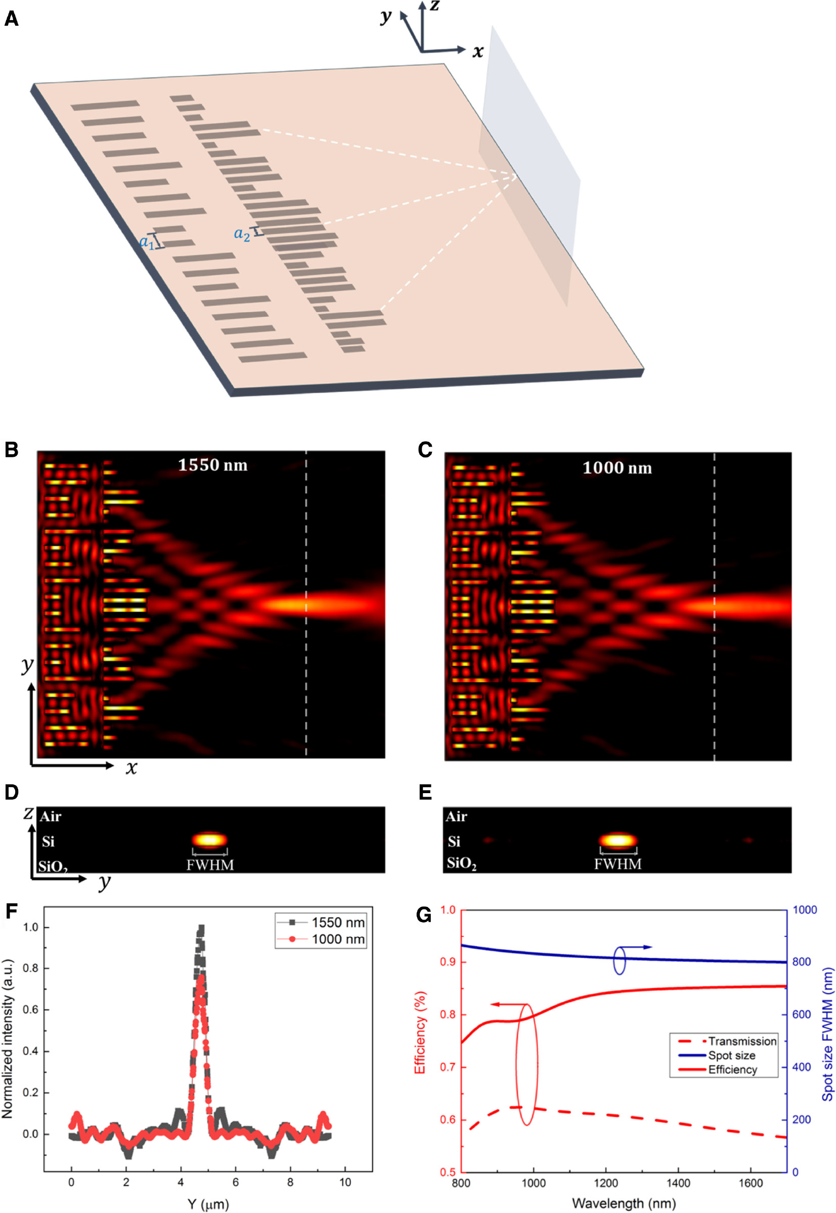
Simulation results of the proposed dispersionless metalens.
(A) Schematic diagram of the dispersionless metalens. (B and C) |Ey|2, in-plane (x-y plane), light distribution of the proposed dispersionless metalens at wavelength of 1550 and 1000 nm, respectively. The white line shows the focal plane. (D and E) Cross-section (y-z plane) view of light distribution at the focal plane (x=8 μm) with wavelength of 1550 and 1000 nm, respectively. (F) Spatial distribution curve of light intensity along the y-direction at the focal plane under dual wavelengths. (G) Focusing efficiency, transmission, and spot size of the metalens over the wavelength range of 900 nm.
The final optimized set of length is numerically evaluated. Figure 1B and C shows the light intensity distribution in the x-y plane in the middle of the metalens at the wavelength of 1000 and 1550 nm, respectively. Figure 1D and E shows the corresponding light intensity distribution on the focal plane (y-z plane). The polarization of the input signal light is in the y-direction. The first array of final optimized structure splits the wavefront into several parts and the second array guides each part to the focal plane. The interference between the transmitted wave is carefully adjusted and gets a maximum at the focal point. The metalens is 9.4 μm wide in the y-direction, with a focal length of 8 μm. The center of the focal point for two wavelengths is displaced less than 100 nm, which is far less than the focal length. This shows that the dispersion of the lens is negligible, and the focal plane is considered the same for wavelength of 1550 and 1000 nm. The spot size is defined as the full-width at half-maximum (FWHM) of the focal spot in the cross-section (y-z plane) at the focal plane, and the spot sizes are 830 and 800 nm in the y-direction; for the final optimized metalens, the maximum focusing efficiency can reach 79% and 85% at wavelengths of 1000 and 1550 nm, respectively. The spatial intensity distributions when performing at two wavelengths are overlaid in one plot, showing that the same focus point at different two wavelengths is optimized by the algorithm (Figure 1F). To demonstrate the broadband characteristics of the proposed lens, we have done the simulation results (Figure 1G). Within the 900 nm bandwidth centered at 1250 nm, the focusing efficiency is more than 75% and the transmission is more than 56%. In addition, the change of focusing efficiency and transmission is less than 10% over the whole wavelength range. Meanwhile, the focal spot size varies within 60 nm.
To verify our theoretical design, we experimentally demonstrated the performance of the dispersionless metalens. The size of input coupling grating is 10×9.4 μm, whereas the size of the output grating is 5×5 μm. Periodic grating couplers usually have a relatively narrow bandwidth compared to aperiodic grating couplers, which cannot achieve high coupling efficiency at multiple wavelengths concurrently. Here, the aperiodic gratings are designed to have considerable excitation efficiency for two wavelengths simultaneously to ensure the validity of measurements. The gratings are designed to have considerable excitation efficiency for two wavelengths simultaneously. The grating for input coupling consists of 20 slots, and the grating for output coupling consists of 10 slots. GA is used to determine the location distribution of each slot. The population size is 40 for both models, and the generations are 20. The optimizing steps are the same as the above. After two steps of optimization, we got the input coupling grating with excitation efficiency of 11.2% and 9.6% for 1000 and 1550 nm, respectively, and the output coupling grating with coupling efficiency of 22.8% and 20.4% for these two wavelengths, respectively. In our experiment, the metalens sample is etched in a 220-nm-thick upper silicon film of a double-side polished silicon-on-insulator wafer using the scanning electron microscopy (SEM) and focused ion beam dual-beam system (FEI Helios NanoLab 600i). For effective etching, different beam current is used for different structure on the metalens device. The beam currents of the central structures, coupling gratings, and transmission waveguides are 7.7, 24, and 80 pA, respectively, with the same ion beam voltage of 30 kV. The SEM image of this metalens structure is shown in Figure 2A. Ten discretized waveguides are placed on the output plane parallelly to obtain the intensity distribution of output signals. Metalens devices are tested on an optical fiber-coupled experimental system. The supercontinuum wave laser system (SC-5, YSL) is used as the light source. In order to realize the effective coupling, we adjust the position and the angle of the launching taper to optimize near-field coupling with the input coupling port of metalens devices. The second nanotaper is moved to different output coupling ports successively to gather output signals. Then, the output signals are collected with a spectrometer (model Andor 303i) for the analysis of required wavelengths. In Figure 2B and C, the measured intensity distribution of output signal at two wavelengths is consistent with the simulation results, which shows that the dispersionless metalens is indeed realized experimentally. The background intensity is stronger in the experiment than in the simulation, which may be caused by the difference in boundary condition. In the simulation, we use scattering boundary condition on the lateral side of the model to avoid the reflection, whereas, in the experiment, the reflected light is coupled into the device, inevitably leading to a brighter background. In addition, the deviation of the peak position comes from the finite number of output waveguides as well as the imperfect sample fabrication.

Experimental realization of the dispersionless metalens.
(A) Overall view of the SEM image of the dispersionless metalens. (Insert, i) Two cascaded arrays of air slots in the silicon film, the characteristic structure of the metalens. (ii) Optimized aperiodic input coupling grating, which can couple input signals at 1550 and 1000 nm efficiently. (iii) Optimized aperiodic output coupling grating, which has high coupling efficiency for both wavelengths. (B and C) Measured distribution of light intensity on focal plane along the y-direction compared to simulation results at wavelength of 1550 and 1000 nm, respectively.
2.2 4f optical processing system and on-chip nanophotonic convolver
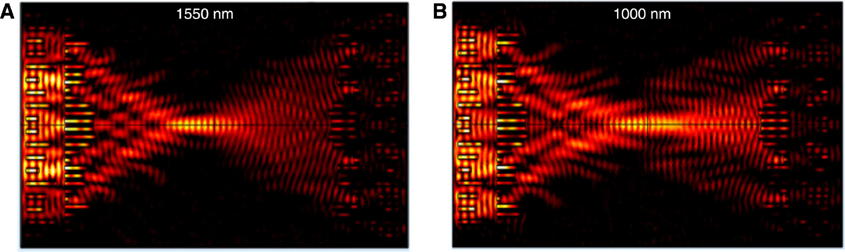
Using two metalenses above, we build an on-chip 4f optical processing system. When giving an input plane at a distance d from a one-dimensional metalens with focal length f and the input signal on the input plane can be written as f(y), the output signal on the focal plane can be given as
When there is no extra structure with its transmission function on the third plane, the focal plane of the first metalens, the transmission function can be written as t=1, so the output u(y″) is proportional to f(–y). When the input is symmetrical about origin, the output will be the same as input if normalized. The numerically results of this situation with two wavelengths are shown in Figure 3A and B. The output light distribution concentrates at five gaps between the air slots, and this is the same case for the input signal at both two wavelengths. The well-matched intensity distribution between the input and the output means that the proposed 4f optical processing system has been established well.
4f optical processing system.
(A and B) When there is no other structure in the third plane (focal plane of the first metalens), i.e. the transmission function is t=1, in-plane light distribution |Ey|2 of the proposed 4f system at wavelength of 1550 and 1000 nm, respectively.
Then, we test the third plane with the random given structure whose SEM images are shown in Figure 4A and B. The transmission of the structure can be acquired numerically when giving an input of the plane wave. By comparing the electric field distribution before and after the plane, we can get the intensity transmission and the phase shift. Using the transmission curve (Figure 4C and D), we can get the theoretical convolution result through numerical calculation when giving an input of a normalized Gaussian function with a characteristic width of 2 μm. The SEM image of the on-chip nanophotonic convolver is shown in Figure 4C, and the feature size of the convolver is 24×9.4 μm. As shown in Figure 4E and F, the output light intensity distribution reflects the spatial convolution operation result of the normalized incident signal and the transmission curve of the given structure. We compare the experimental distribution to the simulation and theoretical results to show the good performance of the proposed convolver. Note that the difference between the simulation results and the theoretical calculation results may come from the existence of a certain interference between the two lenses, resulting in a slight change of the focal length. Here, we define the deviation of the measured output results from the theoretical results as

Realization of on-chip nanophotonic convolver.
(A) Overall view of the SEM image of the proposed convolver. (B) Characteristic structure of this device. The part enclosed by the green dotted frame is the given structure with its transmission function t(y′). (C and D) Spatial transmission distribution curve of the given structure acquired by numerical simulation when giving an input of the plane wave at two wavelengths of 1550 and 1000 nm. (E and F) Measured spatial convolution results along the y-direction compared to the simulation and theoretical results at wavelength of 1550 and 1000 nm, respectively.
3 Conclusion
In this paper, we proposed and experimentally demonstrated a dispersionless metalens for dual wavelengths, a 4f optical processing system, and the on-chip nanophotonic convolver based on silicon metasurface. Instead of the traditional intuitive-based manual adjustment of structural parameters, we used GA of inverse design to optimize the structural parameters, making the concurrent optimization under dual wavelengths more efficient and simpler. The dispersionless metalens owns high transmission and focusing efficiency at two wavelengths of 1000 and 1550 nm. The proposed convolver exhibits spatial convolution operation on the given function at dual wavelengths parallelly. This strategy can be used to execute other convolution operations simply by changing the desire function on the focal plane. Furthermore, this proposal has the potential of being further extended to deal with more complex computing tasks using wavelength multiplexing.
Acknowledgments
This work was supported by the National Key Research and Development Program of China (grant 2018YFB2200403), the National Natural Science Foundation of China (funder id: http://dx.doi.org/10.13039/501100001809, grants 61775003, 11734001, 91950204, and 11527901), and the Beijing Municipal Science & Technology Commission (grant Z191100007219001).
References
[1] Salahuddin S, Ni K, Datta S. The era of hyper-scaling in electronics. Nat Electron 2018;1:442–50.10.1038/s41928-018-0117-xSuche in Google Scholar
[2] Brunner D, Soriano MC, Mirasso CR, Fischer I. Parallel photonic information processing at gigabyte per second data rates using transient states. Nat Commun 2013;4:1364.10.1038/ncomms2368Suche in Google Scholar PubMed PubMed Central
[3] Cheng Q, Bahadori M, Glick M, Rumley S, Bergman K. Recent advances in optical technologies for data centers: a review. Optica 2018;5:1354–70.10.1364/OPTICA.5.001354Suche in Google Scholar
[4] Marpaung D, Yao J, Capmany J. Integrated microwave photonics. Nat Photon 2019;13:80–90.10.1038/s41566-018-0310-5Suche in Google Scholar
[5] Wang Z, Li T, Soman A, Mao D, Kananen T, Gu T. On-chip wavefront shaping with dielectric metasurface. Nat Commun 2019;10:3547.10.1117/12.2540979Suche in Google Scholar
[6] Ambs P. Optical computing: a 60-year adventure. Adv Opt Technol 2010;2010:372652.10.1155/2010/372652Suche in Google Scholar
[7] Willner A, Khaleghi S, Chitgarha M, Yilmaz O. All-optical signal processing. J Lightwave Technol 2014;32:660–80.10.1109/JLT.2013.2287219Suche in Google Scholar
[8] Liu S, Cui TJ, Zhang L, et al. Convolution operations on coding metasurface to reach flexible and continuous controls of terahertz. Adv Sci 2016;3:1600156.10.1002/advs.201600156Suche in Google Scholar PubMed PubMed Central
[9] Dominguez A. A history of the convolution operation. IEEE Pulse 2015;6:38–45.10.1109/MPUL.2014.2366903Suche in Google Scholar
[10] Ryan O, Debbah M. Convolution operations arising from Vandermonde matrices. IEEE Trans Inf Theory 2011;57: 4647–59.10.1109/TIT.2011.2145990Suche in Google Scholar
[11] Smith DC. An introduction to distribution theory for signals analysis. Part II. The convolution. Digit Signal Prog 2006;16:419–44.10.1016/j.dsp.2005.10.004Suche in Google Scholar
[12] Yan T, Wu JM, Zhou TK, et al. Fourier-space diffractive deep neural network. Phys Rev Lett 2019;123:023901.10.1103/PhysRevLett.123.023901Suche in Google Scholar PubMed
[13] Malkiel I, Mrejen M, Nagler A, Arieli U, Wolf L, Suchowski H. Plasmonic nanostructure design and characterization via deep learning. Light Sci Appl 2018;7:60.10.1038/s41377-018-0060-7Suche in Google Scholar PubMed PubMed Central
[14] Wiecha PR, Muskens OL. Deep learning meets nanophotonics: a generalized accurate predictor for near fields and far fields of arbitrary 3D nanostructures. Nano Lett 2020;20:329–38.10.1021/acs.nanolett.9b03971Suche in Google Scholar PubMed
[15] Ma W, Cheng F, Liu Y. Deep-learning-enabled on-demand design of chiral metamaterials. ACS Nano 2018;12:6326–34.10.1021/acsnano.8b03569Suche in Google Scholar PubMed
[16] Liu Z, Zhu D, Rodrigues SP, Lee K-T, Cai W. Generative model for the inverse design of metasurfaces. Nano Lett 2018;18:6570–6.10.1021/acs.nanolett.8b03171Suche in Google Scholar PubMed
[17] Ma W, Cheng F, Xu Y, Wen Q, Liu Y. Probabilistic representation and inverse design of metamaterials based on a deep generative model with semi-supervised learning strategy. Adv Mater 2019;3:1901111.10.1002/adma.201901111Suche in Google Scholar PubMed
[18] Peurifoy J, Shen Y, Jing L, et al. Nanophotonic particle simulation and inverse design using artificial neural networks. Sci Adv 2018;4:eaar4206.10.1126/sciadv.aar4206Suche in Google Scholar PubMed PubMed Central
[19] Molesky S, Lin Z, Piggott AY, Jin W, Vucković J, Rodriguez AW. Inverse design in nanophotonics. Nat Photon 2018;12:659–70.10.1038/s41566-018-0246-9Suche in Google Scholar
[20] Yao K, Unni R, Zheng YB. Intelligent nanophotonics: merging photonics and artificial intelligence at the nanoscale. Nanophotonics 2019;8:339–66.10.1515/nanoph-2018-0183Suche in Google Scholar PubMed PubMed Central
[21] Bing S, Peng W, Polson R, Menon R. An integrated-nanophotonics polarization beamsplitter with 2.4 times 2.4 μm2 footprint. Nat Photon 2015;9:378–82.10.1038/nphoton.2015.80Suche in Google Scholar
[22] Lin Z, Liang XD, Loncar M, Johnson SG, Rodriguez AW. Cavity-enhanced second-harmonic generation via nonlinear-overlap optimization. Optica 2016;3:233–8.10.1364/FIO.2015.FM1D.3Suche in Google Scholar
[23] Andkjaer J, Johansen VE, Friis KS, Sigmund O. Inverse design of nanostructured surfaces for color effects. JOSA B 2014;31:164–74.10.1364/JOSAB.31.000164Suche in Google Scholar
[24] Callewaert F, Velev V, Kumar P, Sahakian AV, Aydin K. Inverse-designed broadband all-dielectric electromagnetic metadevices. Sci Rep 2018;8:1358.10.1038/s41598-018-19796-ySuche in Google Scholar PubMed PubMed Central
[25] Sitawarin C, Jin WL, Lin Z, Rodriguez AW. Inverse-designed photonic fibers and metasurfaces for nonlinear frequency conversion. Photon Res 2018;6:B82–9.10.1364/PRJ.6.000B82Suche in Google Scholar
[26] Lin Z, Loncar M, Rodriguez AW. Topology optimization of multi-track ring resonators and 2D microcavities for nonlinear frequency conversion. Opt Lett 2017;42:2818–21.10.1364/OL.42.002818Suche in Google Scholar PubMed
[27] Piggott AY, Lu J, Lagoudakis KG, Petykiewicz J, Babinec TM, Vuckovic J. Inverse design and demonstration of a compact and broadband on-chip wavelength demultiplexer. Nat Photon 2015;9:374–7.10.1038/nphoton.2015.69Suche in Google Scholar
[28] Su L, Piggott AY, Sapra NV, Petykiewicz J, Vuckovic J. Inverse design and demonstration of a compact on-chip narrowband three- channel wavelength demultiplexer. ACS Photon 2018;5:301–5.10.1021/acsphotonics.7b00987Suche in Google Scholar
[29] Sanchis L, Hakansson A, Lopez-Zanon D, Bravo-Abad J, Sanchez-Dehesa J. Integrated optical devices design by genetic algorithm. Appl Phys Lett 2004;84:4460–2.10.1063/1.1738931Suche in Google Scholar
© 2020 Xiaoyong Hu et al., published by De Gruyter, Berlin/Boston
This work is licensed under the Creative Commons Attribution 4.0 International License.
Artikel in diesem Heft
- Editorial
- Editorial on special issue “Metamaterials and Plasmonics in Asia”
- Reviews
- Metamaterials – from fundamentals and MEMS tuning mechanisms to applications
- Large-area metasurface on CMOS-compatible fabrication platform: driving flat optics from lab to fab
- Tip-enhanced photoluminescence nano-spectroscopy and nano-imaging
- Plasmon-enhanced organic and perovskite solar cells with metal nanoparticles
- Plasmonic nanostructures in photodetection, energy conversion and beyond
- Broadband metamaterials and metasurfaces: a review from the perspectives of materials and devices
- Visible to long-wave infrared chip-scale spectrometers based on photodetectors with tailored responsivities and multispectral filters
- Research Articles
- All-metallic geometric metasurfaces for broadband and high-efficiency wavefront manipulation
- Revealing photonic Lorentz force as the microscopic origin of topological photonic states
- Topological edge and corner states in a two-dimensional photonic Su-Schrieffer-Heeger lattice
- Dual-band dichroic asymmetric transmission of linearly polarized waves in terahertz chiral metamaterial
- A conformal transformation approach to wide-angle illusion device and absorber
- A complete phase diagram for dark-bright coupled plasmonic systems: applicability of Fano’s formula
- Optical telescope with Cassegrain metasurfaces
- Smart sensing metasurface with self-defined functions in dual polarizations
- Experimental nanofocusing of surface plasmon polaritons using a gravitational field
- Mechanotunable optical filters based on stretchable silicon nanowire arrays
- Extraordinary optical transmission and second harmonic generation in sub–10-nm plasmonic coaxial aperture
- Particle simulation of plasmons
- AI-assisted on-chip nanophotonic convolver based on silicon metasurface
- Hybrid organic-inorganic perovskite metamaterial for light trapping and photon-to-electron conversion
- Proposed method for highly selective resonant optical manipulation using counter-propagating light waves
- Temperature-dependent dark-field scattering of single plasmonic nanocavity
- On-chip trans-dimensional plasmonic router
- Chaotic photon spheres in non-Euclidean billiard
- Systematic studies for improving device performance of quantum well infrared stripe photodetectors
- Wide gamut, angle-insensitive structural colors based on deep-subwavelength bilayer media
- Generation of terahertz vector beams using dielectric metasurfaces via spin-decoupled phase control
- Loss and gain in a plasmonic nanolaser
- Flexibly tunable surface plasmon resonance by strong mode coupling using a random metal nanohemisphere on mirror
- Dynamic tuning of enhanced intrinsic circular dichroism in plasmonic stereo-metamolecule array with surface lattice resonance
- Directing Cherenkov photons with spatial nonlocality
- Narrow-frequency sharp-angular filters using all-dielectric cascaded meta-gratings
- Reconfigurable topological waveguide based on honeycomb lattice of dielectric cuboids
- Optical spin-dependent beam separation in cyclic group symmetric metasurface
- Helicity-delinked manipulations on surface waves and propagating waves by metasurfaces