Mechanotunable optical filters based on stretchable silicon nanowire arrays
-
Yeong Jae Kim
 ,
Young Jin Yoo
,
Young Jin Yoo
 and
Young Min Song
and
Young Min Song

Abstract
Nano-structural optical filters embedded in elastomers having high mechanical tunability provide the geometric degree of freedom for selective light manipulation. The active control of spectral information in typical structural optical filters is highly limited due to the substrate rigidity. Herein, we present mechanochromic transmissive optical filters by employing flexible and stretchable polymer-embedded silicon nanostructures. Si-based nanowire arrays (Si-NWAs) have been introduced to exhibit parametric resonance characteristics by controlling the period and/or diameter. Furthermore, the spectral shift phenomenon by increased diffraction efficiency was observed after the application of a uniaxial tensile force, which depends on the period of Si-NWAs with a large index contrast between the silicon nanowire and elastomer. The strain-sensitive properties of tunable Si-NWAs filters induced by light diffraction were calculated by simulation based on wave optics. The spectral tunability and light filtering features were simply demonstrated by stretching the Si-NWAs’ optical filters. Our proposed structure provides potential opportunities for a wide variety of applications, including dynamic color display, visual strain sensor and anti-counterfeiting.
1 Introduction
Optical filters that are used to handle light are simple but highly versatile materials that have recently been applied in many light-based fields, including displays, sensors and photovoltaics in today’s rapidly developing technology-centric world [1], [2], [3], [4], [5], [6]. Especially, the color filters are actively used as representative optical filters in the visible light region recognized by the human eye [7], [8]. The structural color filters are emerging as a core technology in diverse optic components due to several advantages, such as high spatial resolution, long-term stability (including resistance to heat/photolysis) and wide color gamut via light resonance design compared to conventional dyes and pigment color filters [9], [10], [11]. These structure-based color filters have been implemented in various forms, including Fabry-Pérot interferometers, grating structures, plasmon resonators and nanowires (NWAs) [12], [13], [14], [15], [16]. In particular, Si-based nanowire arrays (Si-NWAs) have been introduced as optical color filters that have leaky/guided resonance modes in a specific wavelength range. Their quantitative parameters, such as period and diameter, can be elaborately designed by nanofabrication techniques [17].
However, the aforementioned structural color filters are highly static in terms of spectral tunability due to the rigid substrates used during their production; hence, their applications are strictly limited. In addition, the high-cost and complex production process of delicate nanofabrication using e-beam lithography and laser lithography hinders the advantages of resonant design selectivity by the nanostructures [18], [19]. As a smarter approach, flexible color filters, including photonic crystals, have been recently reported by exploiting polymeric substrates, such as polyethylene terephthalate (PET) or polydimethylsiloxane (PDMS), which provide flexibility [20], [21], [22], [23], [24], [25], [26], [27], [28]. These flexible filters have a wide range of potential applications in combination with flexible/wearable devices requiring conformal adhesion to complex surfaces and/or unique form factors with reduced thickness [29], [30], [31], [32], [33], [34]. Meanwhile, even with NWAs, flexible color filters embedded in PDMS have also been reported [35]. Along with Si-based NWAs, the previous results showed an extended color gamut with transferable Si-NWAs filters attached to resonant structures, such as ultra-thin films and metal-insulator-metal (MIM) resonators, and successfully demonstrated anti-counterfeiting structures using unique diffraction characteristics [36].
Despite the fluent development of Si-NWAs as flexible color filters, only a few studies have investigated the criteria of mechanically adjustable optical information. For more practical utilization, herein, with PDMS-embedded Si-NWAs, we present the static/dynamic spectral tunability of Si-NWAs as a function of the structural periodicity. Their color tuning property was observed according to spectral change when a uniaxial tensile force was applied. The distributions of nanowire arrays critically affect their spectral/colorimetric response due to light diffraction properties within a specific period range [37]. The diffraction efficiency of the proposed structure is varied depending on the strain ratio. The tunable optical filtering feature is proven with diverse LEDs, which have different peak wavelengths. The diffraction characteristics are calculated by rigorous coupled-wave analysis (RCWA) while considering the mechanical properties of the PDMS medium. Moreover, dual notch filters are easily designed and accomplished by stacking two Si-NWAs filters with different resonant features.
2 Results and discussion
Figure 1A illustrates a schematic of the mechanically stretchable silicon nanowire arrays (MSNWAs) in an elastomeric polydimethylsiloxane for tunable optical filters. The optical response transition of the MSNWAs through the geometric transformation is caused by applying a uniaxial stretching force. The Si nanowires exhibit intrinsic colors in the bare state due to leaky/guided modes, which feature different wavelength selectivity depending on their size of geometry (Figure S1). Figure 1B shows that the transmittance dip shifts toward longer wavelengths depending on the strain ratio. The optical spectrum can be modulated by the distance between nanowire arrays. The corresponding transmitted color representations are calculated by (Figure S2) in Figure 1B, right. To visually confirm the light filtering characteristics, the proposed light filter was investigated on the white light of a xenon lamp, and certain wavelengths were blocked by MSNWAs (Figure 1C). As a result, the transmitted light shifts from yellow to magenta when the MSNWAs filter is stretched (Figure 1C). Figure 1D presents photographs of the Si nanowires embedded in the PDMS polymer (left), bright-field optical microscope images of bare MSNWAs (right, top) and the images when stretched (right, bottom). Due to these two-dimensional grating characteristics, the diffraction patterns are observed on the surface. By applying a mechanical force, this photonic film is “stretched” because of the pliability of the PDMS medium. We used optical microscopy to observe the arrangement of the nanostructure during the stretching. Before stretching the structure, the same horizontal and vertical spacing was observed. The proposed structure has a periodic nanowire array in the form of a square. After stretching, the transverse axis increased and the longitudinal axis decreased. This is determined by the Poisson’s ratio of the PDMS material with a value of 0.5 [38]. The chromatic information was calculated from the measured transmittance spectra by using MATLAB (Mathworks, Inc.) software (Figure 1E). The color coordinates were shifted in the clockwise direction as a result of the increased strain ratio.
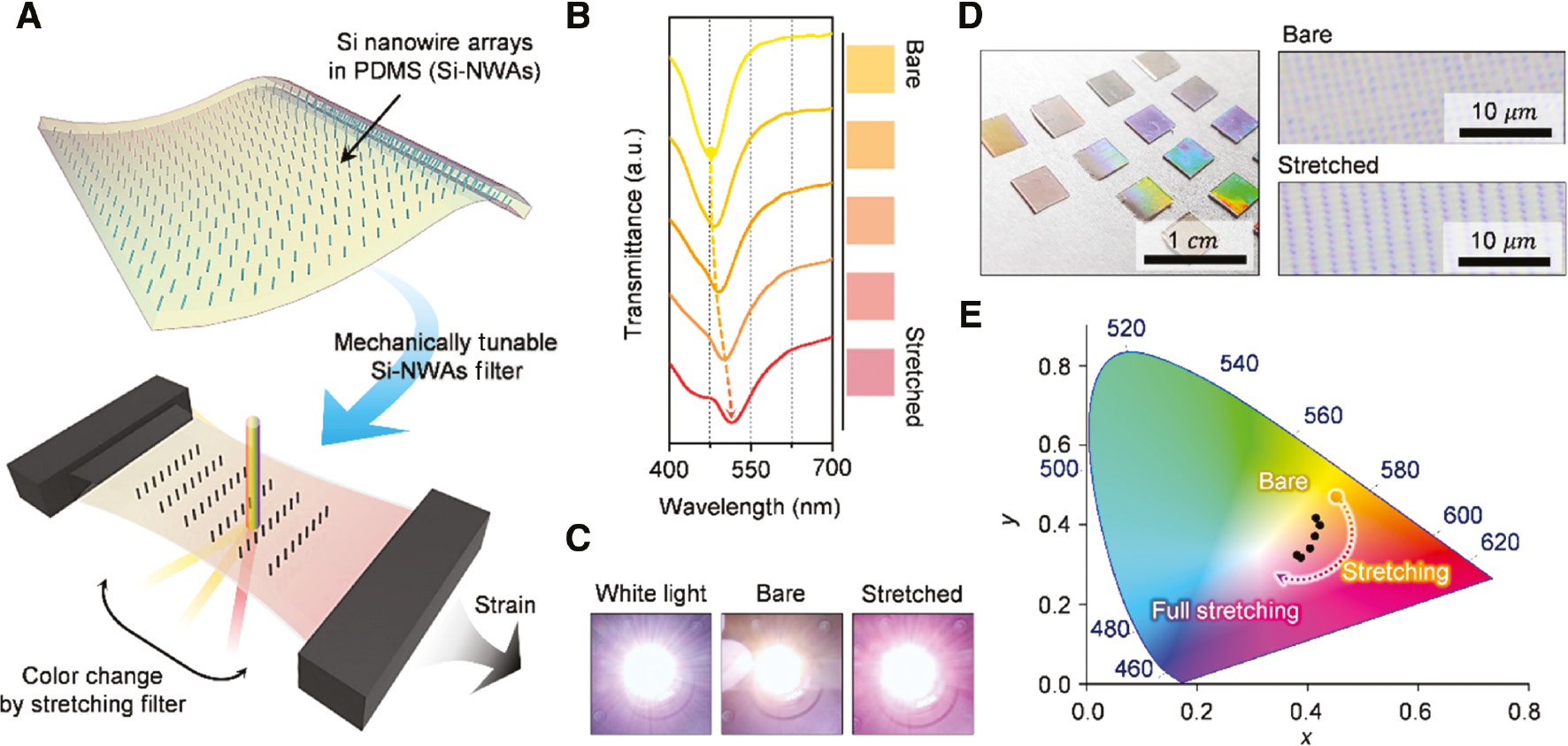
The mechanically tunable Si nanowire optical filter with spectral tunability.
(A) Schematic illustration of the tunable nanowire color filter. (B) Transmittance curves of the Si-NWAs and color representation of the stretched Si-NWAs. (C) Tunable transmissive color filter properties comparing the bare and full stretching samples. (D) Photographs of the Si-NWAs with different periods and diameters (left), microscope images before and after stretching Si-NWAs (right). (E) The color representations of the bare and stretching samples.
Figure 2A shows the fabrication processes used to prepare the MSNWAs. The oxide layer with ~200 nm thickness was formed on a silicon wafer by a thermal annealing process. Then, the KrF excimer laser lithography was performed to fabricate the nanodisc arrays (Nikon Inc., KrF scanner S203-B). The exposed silicon area was anisotropically etched for 2 μm height by a reactive ion etching (RIE) process (Oxford Plasmalab 133). The oxide residues on a silicon wafer were removed by the application of hydrofluoric acid (HF). The thermal oxidation process and HF wet etching treatments were repeated to precisely tailor the silicon nanowire diameters to 60 nm. The PDMS polymers, utilized as substrates, are capable of repeated mechanical bending and are characterized by hundreds of micrometers in thickness and millimeter to centimeter scale bend radii [39]. The PDMS was mixed with a base elastomer and a cross-linking agent ratio of 5:1 (Sylgard 184, Dow Corning, USA) to provide curing conditions. In order to eliminate air bubbles in the mixed PDMS, the polymer blend was placed in a vacuum chamber for 30 min. Then, the PDMS was spin-coated on the silicon nanowire substrate (500 rpm for 30 s). Afterward, the spin-coated PDMS on the silicon nanowire substrate was thermally annealed at 230°C for 2 h by a hot plate. The PDMS-embedded Si-NWAs were obtained by peeling off the nanowire substrate using a blade (NT-Cutter, BSC-21P). Figure 2B shows the SEM images that provide geometric information of the cross-section (top, left) and top-views (top, right). The diameters in the 60–110 nm range produce resonances in the visible spectral range. As a result, multi-colored optical filters can be achieved by adjusting the shape of the nanostructure (Figure 2B, bottom). Figure 2C illustrates the stacking process of two different silicon nanowire arrays for multi-band optical filters. As can be seen, the transmittance dip of each layer was maintained. Meanwhile, the MSNWAs were stretched using a home-made stretching device (Figure S3), as shown in Figure 2D.
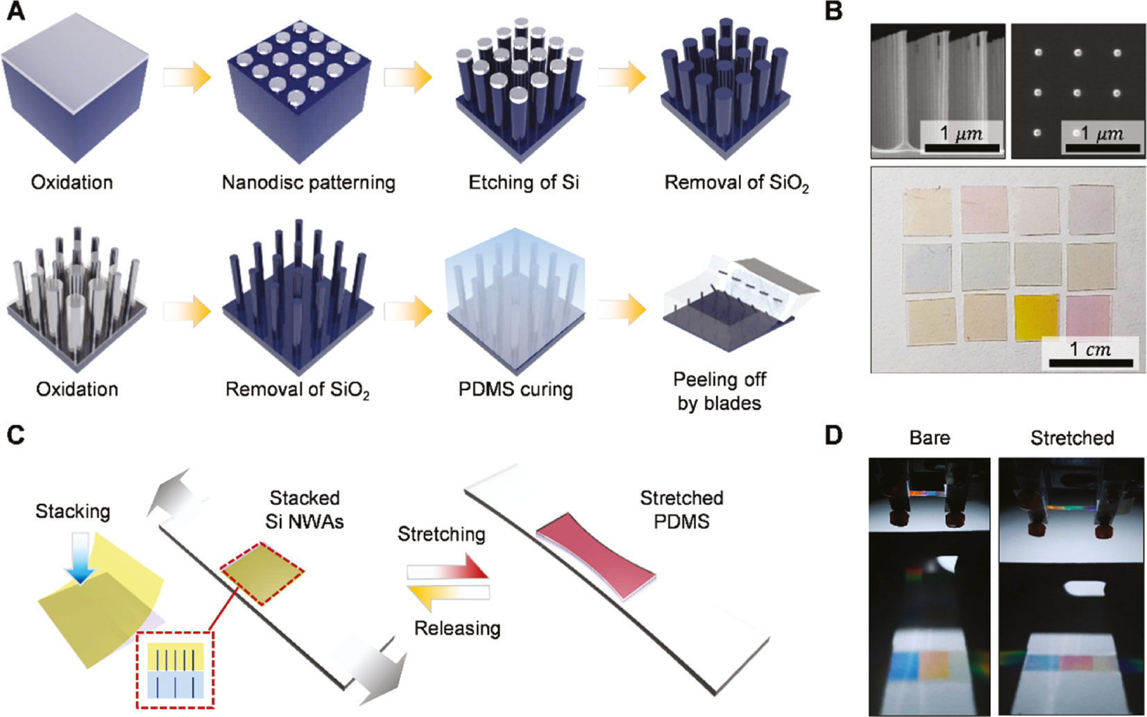
The fabrication method for the mechanically tunable Si-NWA optical filter.
(A) Schematic illustration of the fabrication process for Si-NWAs. (B) SEM images of Si-NWAs (top) and photographs of Si-NWAs with different periods and diameters (bottom). (C) Stacking two different Si-NWAs filters. (D) Photographs of Si-NWAs filters with applying strain.
Figure 3A shows the schematic diagram of the optical simulation to interpret the transmittance dip shifts of stretched silicon nanowire optical filters. The three-dimensional rigorous coupled-wave analysis (3D RCWA) was performed by considering a Poisson’s ratio. A commercial software tool (DiffractMOD, RSoft Design Group, USA) was used to understand the light propagation properties for the various geometric parameters of the proposed structure. Depending on the vertically arranged nanowire array, the periodic boundaries for optical simulation were taken into account with 10th order diffraction orders. To consider the spectral information, an un-polarized light diffracted pattern and electric field profiles were simulated and the transverse electric and magnetic modes were averaged. The refractive index and extinction coefficients as a function of wavelength were considered from the previous literature [40], [41]. The Poisson’s ratio for PDMS is 0.5, which is a negative transverse to lateral strain ratio. The stretching in the x-direction reduces the length in the y-direction, which means a uniaxial strain onto PDMS converts the square geometry into a rectangle (Figure 3A).
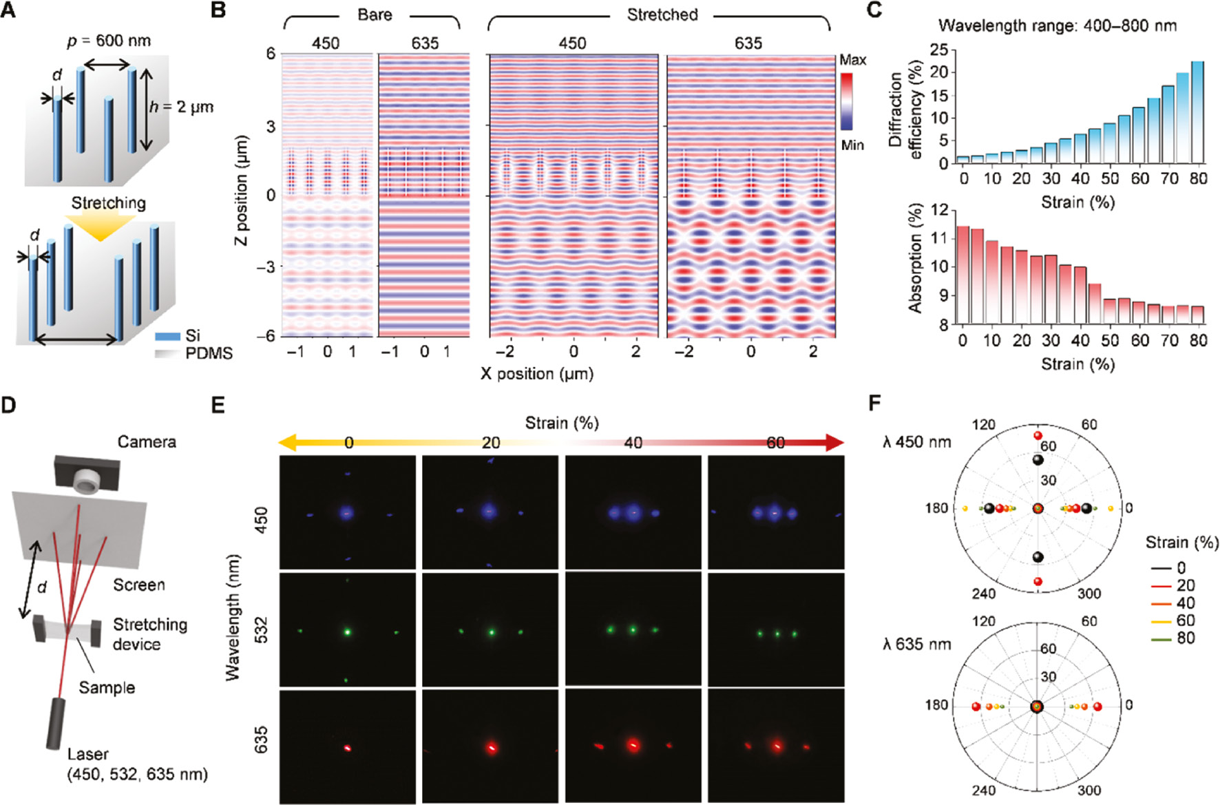
The simulation and experimental results for light diffraction properties.
(A) Schematic illustration of the Si-NWAs embedded in PDMS. (B) The real part of electric-field distributions from three-dimensional finite-difference time-domain simulations. (C) Diffraction efficiency and averaged absorption depending on the applied strain with the wavelength range of 400–800. (D, E) Experimental setups and photographs for diffraction patterns. (F) Simulated diffraction patterns with the period 600 nm of Si-NWAs.
Next, bare and stretched filters were simulated to determine the electric field propagation at 450 nm and 635 nm wavelengths (Figure 3B). In the bare (un-stretched) state, the diffraction patterns were observed at the 450 nm wavelength. Meanwhile, it was observed that the light of 635 nm wavelength proceeded without changing the light path. As the period of the Si-NWAs changed (stretched state), the diffracted light of 635 nm wavelength is observed, indicating that the diffraction could be adjusted according to the degree of stretching. As shown in Figure 3C, as broadband diffraction becomes possible according to increased strain ratio, the averaged diffraction efficiency increases. In certain periodicities of Si-NWAs, the lights are concentrated by leaky modes [42]. The reduced absorption was calculated by the deformed arrangement of the MSNWAs (Figure S4). The experimental setup schematic is illustrated to confirm the diffraction pattern depending on the three wavelengths (Figure 3D). The stretchable nanowire filter mounted on the stretching device is located between the blue, green and red lasers (wavelengths of 450, 532 and 635 nm, respectively) and a screen. The diffraction patterns were also respectively obtained for bare (un-stretched), 20%, 40% and 60% stretched samples (Figure 3E). In the case of the blue laser, narrower-angle diffraction occurred compared with the red and green lasers. After stretching, the angle of the first order decreased in the pulling direction. The red laser at 635 nm passed straight through without diffraction. Above 40% of the stretching, the first-order diffraction was observed. Figure 3F shows the calculated diffraction patterns at wavelengths of 450 nm and 635 nm. The diffraction pattern is determined by the arrays of nanostructure [43]. The patterns obtained from the 3D RCWA simulation are similar to the experimental results. The improvement of the diffraction efficiency of the first-order spectrum is observed to be in good agreement with the experimental results.
Meanwhile, the light-emitting diodes (LEDs) with different wavelengths were prepared to demonstrate the band-stop properties of the stretchable nanowire array filter. Figure 4A exhibits the schematics for band-stop filtering experiments with the diverse LED arrays. The center wavelength peaks for the letters “GIST” are 460, 505, 555 and 605 nm, respectively. The clear GIST image was achieved without a nanowire filter as shown in Figure 4B. With a bare Si nanowire filter, the blue light for “G” is rejected due to the 460 nm wavelength band-stop properties. In the stretched nanowire arrays with the period of 600 nm, the transmittance dip shifts toward the longer region. The blocked blue light is observed in the stretched optical filter. To block the red light (605 nm), the nanowires having a diameter of 90 nm and a period of 1250 nm were developed by stacking the existing nanowires.
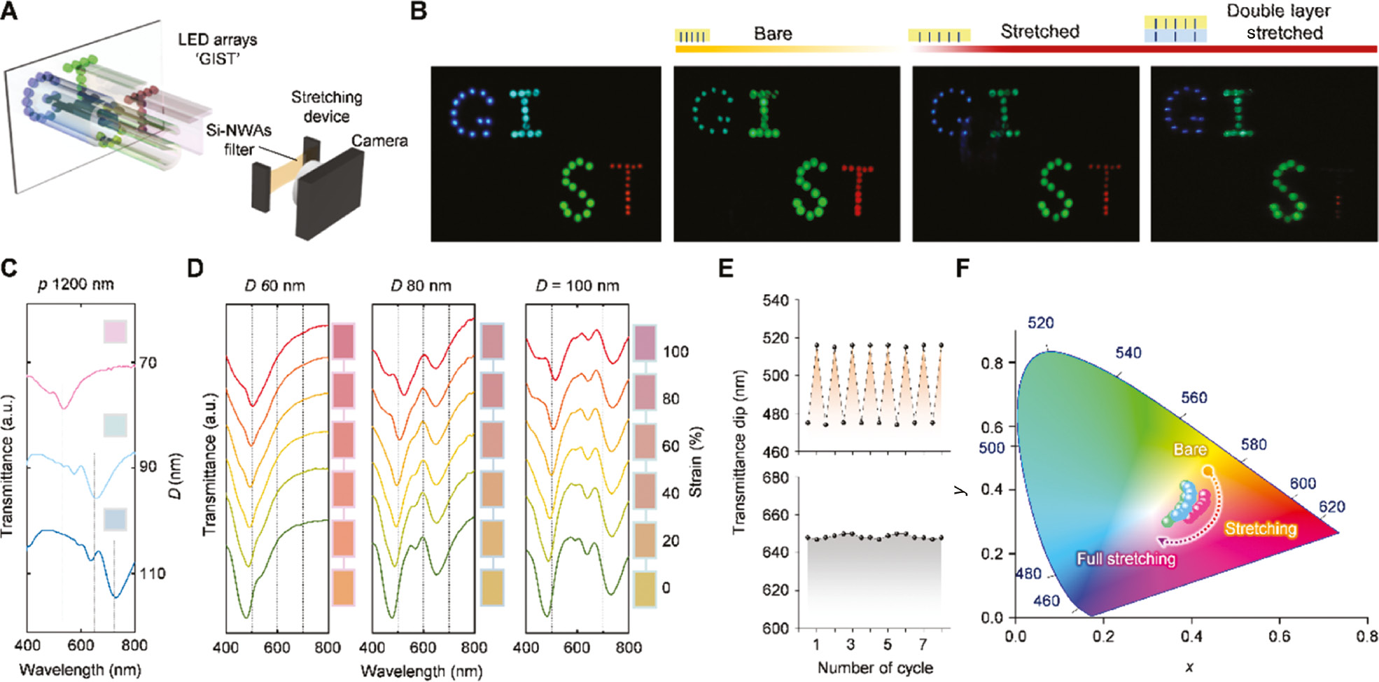
The optical filtering features and strain-induced spectral tunability.
(A) Schematic illustration of the experimental setups for optical filters. (B) Photographs of “GIST” lettered LED arrays and optical filter experimental results. (C, D) The transmittance of the Si-NWAs and color representation depending on the strain ratio. (E) Transmittance dip after the strain cycle of the Si-NWAs with periods of 600 nm (top) and 1200 nm (bottom). (F) Color coordinates for the double-layered MSNWAs.
The nanowires have a linear combination property and maintain a resonance dip when two different filters are overlapped. Therefore, a band-stop filter with two or more dips can be implemented through very simple stacking. These fabricated Si nanowires have been experimentally demonstrated to have wavelength selectivity as the diameter increases due to HE11 mode of the leaky and guided modes. We experimentally fabricated Si nanowire embedded in the PDMS for different diameters and periods and then measured their transmission spectra. To determine the period dependency, the 1200 nm period of the Si-NWAs with three different diameters of 60, 80 and 100 nm were used in these experiments (Figure 4C). The strain at the period 600 nm of silicon nanowire was set from 0%–100%. The optical spectrum can be adjusted according to the applied strain force. The creation of the transmittance dips in the double-layered structures is thus observed (Figure 4D). Unlike Si nanowires with a period of 600 nm, those with a period of 1200 nm exhibit no significant change in the diffraction efficiency and the transmittance dip before and after stretching (Figure S5). Therefore, the spectral shift critically affects the periodicity of the nanostructure. Furthermore, as a diffraction-based resonator, the MSNWAs exhibit angular selective response in consideration of angle dependency with zeroth order diffraction (Figure S6). The transmittance dip for two different periodic samples was measured according to the number of strain cycles as shown in Figure 4E. Results show that the optical performances are maintained despite the air gaps between filters or the swapping of two filters (Figure S7). We thus confirmed that the changed dips occur in only 600 nm periodicity of Si nanowire according to the strain ratio, whereas the 1200 nm periodicity of Si nanowire is maintained when the strain force is applied. The fine-tuned colors were estimated from these measured transmittance spectra as shown in Figure 4F. Results show that the initial colors change when the strain ratio of the MSNWAs increases in the clockwise direction.
3 Conclusions
In conclusion, a strategy to develop mechanically tunable band-stop optical filters is demonstrated by uniaxially stretching the MSNWAs. The pliable PDMS polymer was used as the stretchable medium. The periodic deformation of nanostructures improved the diffraction efficiency. The optical spectrum shifted depending on the strain ratio in the MSNWAs, which can be attributed to the increased spacing between the Si-NWAs. The diffraction characteristics demonstrated that the diffraction order was observed in the 635 nm red laser both in the simulation and experimental results. The tunability and light filtering features at the specific wavelengths were confirmed by stretching the MSNWAs for various LED arrays.
The proposed conceptual demonstration by manually induced mechanical deformation provides a key solution for the extended future application of Si-NWAs. For realistic applications, through a multi-axial approach with automated mechanical deformation, our scheme can be developed as a dynamic visual application, including a display, filter and sensor. With the independent wavelength selectivity for Si-NWAs, the different MSNWA combinations can be utilized as multiband transmissive filters. Using these features, we believe that mechanically tunable applications, such as strain sensitive color filter, light diffuser and colorimetric sensor applications, can be achieved.
Acknowledgments
This work was supported by the Institute for Information and Communications Technology Promotion (IITP) (Grant No. 2017000709), the Creative Materials Discovery Program through the National Research Foundation of Korea (NRF) funded by the Korean government (MSIP) (Grant Nos. NRF2018M3D1A1058997, 2018H1A2A1060954 and 2018R1A4A1025623, Funder Id: http://dx.doi.org/10.13039/501100003725), the GIST Research Institute (GRI) grant funded by the GIST in 2020, Funder Id: http://dx.doi.org/10.13039/501100002582, the Korea Institute of Energy Technology Evaluation and Planning (KETEP) and by the Ministry of Trade, Industry and Energy (MOTIE) of the Republic of Korea (Grant No. 20183010014310, Funder Id: http://dx.doi.org/10.13039/501100007053).
References
[1] Harbers G, Bierhuizen SJ, Krames MR. Performance of high power light emitting diodes in display illumination applications. J Disp Technol 2007;3:98–109.10.1109/JDT.2007.894384Search in Google Scholar
[2] Yokogawa S, Burgos SP, Atwater HA. Plasmonic color filters for CMOS image sensor applications. Nano Lett 2012;12:4349–54.10.1021/nl302110zSearch in Google Scholar PubMed
[3] Meng J, Cadusch J, Crozier KB. Detector-only spectrometer based on structurally-colored silicon nanowires and a reconstruction algorithm. Nano Lett 2020;20:320–8.10.1021/acs.nanolett.9b03862Search in Google Scholar PubMed
[4] Park HJ, Xu T, Lee JY, et al. Photonic color filters integrated with organic solar cells for energy harvesting. ACS Nano 2011;5:7055–60.10.1021/nn201767eSearch in Google Scholar PubMed
[5] Lee KT, Lee JY, Seo S, Guo LJ. Colored ultrathin hybrid photovoltaics with high quantum efficiency. Light Sci Appl 2014;3:e215.10.1038/lsa.2014.96Search in Google Scholar
[6] Zhang M, Li S. Controllable liquid colour-changing lenses with microfluidic channels for vision protection, camouflage and optical filtering based on soft lithography fabrication. Springerplus 2016;5:1.10.1186/s40064-016-2231-4Search in Google Scholar PubMed PubMed Central
[7] Diest K, Dionne JA, Spain M, Atwater HA. Tunable color filters based on metal− insulator− metal resonators. Nano Lett 2009;9:2579–83.10.1021/nl900755bSearch in Google Scholar PubMed
[8] Li Z, Butun S, Aydin K. Large-area, lithography-free super absorbers and color filters at visible frequencies using ultrathin metallic films. ACS Photonics 2015;2:183–8.10.1021/ph500410uSearch in Google Scholar
[9] Flauraud V, Reyes M, Paniagua-Dominguez R, et al. Silicon nanostructures for bright field full color prints. ACS Photonics 2017;4:1913–9.10.1021/acsphotonics.6b01021Search in Google Scholar
[10] Galinski H, Favraud G, Dong H, et al. Scalable, ultra-resistant structural colors based on network metamaterials. Light Sci Appl 2017;6:e16233.10.1038/lsa.2016.233Search in Google Scholar PubMed PubMed Central
[11] Wang H, Wang X, Yan C, et al. Full color generation using silver tandem nanodisks. ACS Nano 2017;11:4419–27.10.1021/acsnano.6b08465Search in Google Scholar PubMed
[12] Yang Z, Zhou Y, Chen Y, et al. Reflective color filters and monolithic color printing based on asymmetric Fabry–Perot cavities using nickel as a broadband absorber. Adv Opt Mater 2016;4:1196–202.10.1002/adom.201600110Search in Google Scholar
[13] Yoo YJ, Lim JH, Lee GJ, et al. Ultra-thin films with highly absorbent porous media fine-tunable for coloration and enhanced color purity. Nanoscale 2017;9:2986–91.10.1039/C6NR08475CSearch in Google Scholar
[14] Wen L, Chen Q, Hu X, et al. Multifunctional silicon optoelectronics integrated with plasmonic scattering color. ACS Nano 2016;10:11076–86.10.1021/acsnano.6b05960Search in Google Scholar PubMed
[15] Kim DH, Yoo YJ, Ko JH, et al. Standard red green blue (sRGB) color representation with a tailored dual-resonance mode in metal/dielectric stacks. Opt Mater Express 2019;9:3342.10.1364/OME.9.003342Search in Google Scholar
[16] Zhu L, Kapraun J, Ferrara J, Chang-Hasnain CJ. Flexible photonic metastructures for tunable coloration. Optica 2015;2:255.10.1364/OPTICA.2.000255Search in Google Scholar
[17] Seo K, Wober M, Steinvurzel P, et al. Multicolored vertical silicon nanowires. Nano Letters 2011;11:1851–6.10.1021/nl200201bSearch in Google Scholar PubMed
[18] Wiley BJ, Qin D, Xia Y. Nanofabrication at high throughput and low cost. ACS Nano 2010;4:3554–9.10.1021/nn101472pSearch in Google Scholar PubMed
[19] Liddle JA, Gallatin GM. Nanomanufacturing: a perspective. ACS Nano 2016;10:2995–3014.10.1021/acsnano.5b03299Search in Google Scholar PubMed PubMed Central
[20] Zhao P, Li B, Tang Z, et al. Stretchable photonic crystals with periodic cylinder shaped air holes for improving mechanochromic performance. Smart Mater Struct 2019;28:075037.10.1088/1361-665X/ab1fb8Search in Google Scholar
[21] Meng Y, Zhang S, Wu K, et al. Mechanically tunable bilayer composite grating for unique light manipulation and information storage. Adv Opt Mater 2019;7:1801017.10.1002/adom.201801017Search in Google Scholar
[22] Kim DY, Choi S, Cho H, Sun JY. Electroactive soft photonic devices for the synesthetic perception of color and sound. Adv Mater 2019;31:1804080.10.1002/adma.201804080Search in Google Scholar PubMed
[23] Cho H, Han S, Kwon J, et al. Self-assembled stretchable photonic crystal for a tunable color filter. Opt Lett 2018;43:3501.10.1364/OL.43.003501Search in Google Scholar PubMed
[24] Wang D, Bourgeois MR, Lee WK, et al. Stretchable nanolasing from hybrid quadrupole plasmons. Nano Lett 2018;18:4549–55.10.1021/acs.nanolett.8b01774Search in Google Scholar PubMed
[25] Tseng ML, Yang J, Semmlinger M, et al. Two-dimensional active tuning of an aluminum plasmonic array for full-spectrum response. Nano Lett 2017;17:6034–9.10.1021/acs.nanolett.7b02350Search in Google Scholar PubMed
[26] Steiner AM, Mayer M, Seuss M, et al. Macroscopic strain-induced transition from quasi-infinite gold nanoparticle chains to defined plasmonic oligomers. ACS Nano 2017;11:8871–80.10.1021/acsnano.7b03087Search in Google Scholar PubMed
[27] Lee GH, Choi TM, Kim B, et al. Chameleon-inspired mechanochromic photonic films composed of non-close-packed colloidal arrays. ACS Nano 2017;11:11350–7.10.1021/acsnano.7b05885Search in Google Scholar PubMed
[28] Yang A, Hryn AJ, Bourgeois MR, et al. Programmable and reversible plasmon mode engineering. Proc Natl Acad Sci USA 2016;113:14201–6.10.1073/pnas.1615281113Search in Google Scholar PubMed PubMed Central
[29] Yan C, Kang W, Wang J, et al. Stretchable and wearable electrochromic devices. ACS Nano 2014;8:316–22.10.1021/nn404061gSearch in Google Scholar PubMed
[30] Chou HH, Nguyen A, Chortos A, et al. A chameleon-inspired stretchable electronic skin with interactive colour changing controlled by tactile sensing. Nat Commun 2015;6:1.10.1038/ncomms9011Search in Google Scholar PubMed PubMed Central
[31] Wang JL, Lu YR, Li HH, et al. Large area co-assembly of nanowires for flexible transparent smart windows. J Am Chem Soc 2017;139:9921–6.10.1021/jacs.7b03227Search in Google Scholar PubMed
[32] Ko JH, Yoo YJ, Kim YJ, et al. Flexible, large-area covert polarization display based on ultrathin lossy nanocolumns on a metal film. Adv Funct Mater 2020;1908592.10.1002/adfm.201908592Search in Google Scholar
[33] Li K, Zhang Q, Wang H, Li Y. Red, green, blue (RGB) electrochromic fibers for the new smart color change fabrics. ACS Appl Mater Interfaces 2014;6:13043.10.1021/am502929pSearch in Google Scholar PubMed
[34] Yi H, Lee SH, Ko H, et al. Ultra-adaptable and wearable photonic skin based on a shape-memory, responsive cellulose derivative. Adv Funct Mater 2019;29:1902720.10.1002/adfm.201902720Search in Google Scholar
[35] Kim YJ, Yoo YJ, Lee GJ, et al. Enlarged color gamut representation enabled by transferable silicon nanowire arrays on metal–insulator–metal films. ACS Appl Mater Interfaces 2019;11:11849–56.10.1021/acsami.8b21554Search in Google Scholar PubMed
[36] Song HS, Lee GJ, Yoo DE, et al. Reflective color filter with precise control of the color coordinate achieved by stacking silicon nanowire arrays onto ultrathin optical coatings. Sci Rep 2019;9:1.10.1038/s41598-019-40001-1Search in Google Scholar PubMed PubMed Central
[37] Walia J, Dhindsa N, Khorasaninejad M, Saini SS. Color generation and refractive index sensing using diffraction from 2D silicon nanowire arrays. Small 2014;10:144–51.10.1002/smll.201300601Search in Google Scholar PubMed
[38] Pritchard RH, Lava P, Debruyne D, Terentjev EM. Precise determination of the Poisson ratio in soft materials with 2D digital image correlation. Soft Matter 2013;9:6037.10.1039/c3sm50901jSearch in Google Scholar
[39] Khanafer K, Duprey A, Schlicht M, Berguer R. Effects of strain rate, mixing ratio, and stress–strain definition on the mechanical behavior of the polydimethylsiloxane (PDMS) material as related to its biological applications. Biomed Microdevices 2009;11:503–8.10.1007/s10544-008-9256-6Search in Google Scholar PubMed
[40] Schneider F, Draheim J, Kamberger R, Wallrabe U. Process and material properties of polydimethylsiloxane (PDMS) for Optical MEMS. Sens Actuator A Phys 2009;151:95–9.10.1016/j.sna.2009.01.026Search in Google Scholar
[41] Aspnes DE, Studna AA. Dielectric functions and optical parameters of Si, Ge, GaP, GaAs, GaSb, InP, InAs, and InSb from 1.5 to 6.0 eV. Phys Rev B 1983;27:985–1009.10.1103/PhysRevB.27.985Search in Google Scholar
[42] Wang B, Leu PW. Tunable and selective resonant absorption in vertical nanowires. Opt Lett 2012;37:3756.10.1364/OL.37.003756Search in Google Scholar
[43] Mahpeykar SM, Xiong Q, Wei J, et al. Stretchable hexagonal diffraction gratings as optical diffusers for in situ tunable broadband photon management. Adv Opt Mater 2016;4:1106–14.10.1002/adom.201600122Search in Google Scholar
Supplementary Material
The online version of this article offers supplementary material (https://doi.org/10.1515/nanoph-2020-0062).
© 2020 Il-Suk Kang, Young Min Song et al., published by De Gruyter, Berlin/Boston
This work is licensed under the Creative Commons Attribution 4.0 International License.
Articles in the same Issue
- Editorial
- Editorial on special issue “Metamaterials and Plasmonics in Asia”
- Reviews
- Metamaterials – from fundamentals and MEMS tuning mechanisms to applications
- Large-area metasurface on CMOS-compatible fabrication platform: driving flat optics from lab to fab
- Tip-enhanced photoluminescence nano-spectroscopy and nano-imaging
- Plasmon-enhanced organic and perovskite solar cells with metal nanoparticles
- Plasmonic nanostructures in photodetection, energy conversion and beyond
- Broadband metamaterials and metasurfaces: a review from the perspectives of materials and devices
- Visible to long-wave infrared chip-scale spectrometers based on photodetectors with tailored responsivities and multispectral filters
- Research Articles
- All-metallic geometric metasurfaces for broadband and high-efficiency wavefront manipulation
- Revealing photonic Lorentz force as the microscopic origin of topological photonic states
- Topological edge and corner states in a two-dimensional photonic Su-Schrieffer-Heeger lattice
- Dual-band dichroic asymmetric transmission of linearly polarized waves in terahertz chiral metamaterial
- A conformal transformation approach to wide-angle illusion device and absorber
- A complete phase diagram for dark-bright coupled plasmonic systems: applicability of Fano’s formula
- Optical telescope with Cassegrain metasurfaces
- Smart sensing metasurface with self-defined functions in dual polarizations
- Experimental nanofocusing of surface plasmon polaritons using a gravitational field
- Mechanotunable optical filters based on stretchable silicon nanowire arrays
- Extraordinary optical transmission and second harmonic generation in sub–10-nm plasmonic coaxial aperture
- Particle simulation of plasmons
- AI-assisted on-chip nanophotonic convolver based on silicon metasurface
- Hybrid organic-inorganic perovskite metamaterial for light trapping and photon-to-electron conversion
- Proposed method for highly selective resonant optical manipulation using counter-propagating light waves
- Temperature-dependent dark-field scattering of single plasmonic nanocavity
- On-chip trans-dimensional plasmonic router
- Chaotic photon spheres in non-Euclidean billiard
- Systematic studies for improving device performance of quantum well infrared stripe photodetectors
- Wide gamut, angle-insensitive structural colors based on deep-subwavelength bilayer media
- Generation of terahertz vector beams using dielectric metasurfaces via spin-decoupled phase control
- Loss and gain in a plasmonic nanolaser
- Flexibly tunable surface plasmon resonance by strong mode coupling using a random metal nanohemisphere on mirror
- Dynamic tuning of enhanced intrinsic circular dichroism in plasmonic stereo-metamolecule array with surface lattice resonance
- Directing Cherenkov photons with spatial nonlocality
- Narrow-frequency sharp-angular filters using all-dielectric cascaded meta-gratings
- Reconfigurable topological waveguide based on honeycomb lattice of dielectric cuboids
- Optical spin-dependent beam separation in cyclic group symmetric metasurface
- Helicity-delinked manipulations on surface waves and propagating waves by metasurfaces