All-metallic geometric metasurfaces for broadband and high-efficiency wavefront manipulation
-
Xin Xie


Abstract
Geometric metasurfaces have shown superior phase control capacity owing to the geometric nature of their phase profile. The existing geometric metasurfaces are generally composed of metal-dielectric composites or all-dielectric subwavelength structures. Here, a novel configuration, all-metallic structure, is proposed to achieve broadband and high-performance electromagnetic wavefront manipulation based on the geometric phase. A catenary model is built to describe the optical dispersion and guide the design of metasurfaces. Two metadevices including a beam deflector and a hologram are designed and experimentally demonstrated in the infrared regime, with the measured optical efficiency up to 84% (the simulated efficiency reaches 93%). Compared to previous metal-insulator-metal structures, this approach can realize higher efficiency and broader operating bandwidth owing to its lower ohmic loss. This design strategy is universal and can be easily scaled to any other spectra without complex optimization. Moreover, since metals have excellent mechanical and physical properties, such as good thermal and electrical conductivity, this all-metallic structure may provide a new thinking on interdisciplinary research.
1 Introduction
Artificial metasurfaces are composed of dense arrangements of resonant subwavelength antennas. The resonant nature of the light-matter interaction with such structures affords free control over the local light scattering amplitude and phase [1], [2], [3], [4], [5]. Among the various types of metasurfaces, geometric metasurfaces (GMs) based on the Pancharatnam-Berry (PB) phase have attracted significant interest due to their simple and robust phase control scheme [6], [7]. The beauty of this approach lies in the linear dependence of phase delay Φ on the orientation angle φ of each antenna, i.e. Φ=±2φ; the sign ± denotes the left-handed circular polarization (LCP, +) and right-handed circular polarization (RCP, −), respectively. Therefore, GMs offer straightforward perspectives in designing complex phase-only optical elements, such as beam deflectors [8], [9], vortex plates [10], [11], flat lenses [1], [12], and holograms [13], [14], [15]. High optical efficiency is a long-term pursuit of GMs. According to the geometric phase resulting from the photonic spin-orbit interaction [16], [17], under the illumination of circularly polarized (CP) light, only the cross-polarization component would be imprinted with the additional phase delay. Hence, to achieve high-efficiency GMs, it is essential to obtain high polarization conversion efficiency between the two opposite CP states.
Several approaches have been put forward to improve the conversion efficiency. For transmissive configuration, the single-layer plasmonic metasurfaces have a theoretically predicted upper limit of 25% [18]. Though multilayered structures can realize higher efficiency [19], the thickness, fabrication challenges, and frequency dispersion are significantly enhanced. To further improve the optical efficiency, all-dielectric designs based on titanium oxide (TiO2) [20], [21], gallium nitride (GaN) [22], [23], silicon (Si) [24], etc. are put forward because of their low-loss or even lossless property in visible or infrared spectra. Nevertheless, dielectric metasurfaces usually suffer from high geometric aspect ratios, which seriously increase the fabrication burden. Besides, the Fresnel reflection losses will significantly decrease the optical efficiency of these dielectric materials with high refractive index. For reflective structures, metal-insulator-metal (MIM) designs are typically used to realize efficient polarization conversion [25], [26], [27]. The structures consist of three layers: a ground metal mirror, a dielectric spacer layer, and a top layer of metallic antennas. However, due to the substantial ohmic loss induced by the Fabry-Perot effect of this multilayer configuration, the power efficiency is hard to exceed 80% [26], [27], [28], [29]. Though all-metallic grating-based configurations can dramatically reduce the loss, the large size of pixel (>λ) as well as imperfect splicing at the boundary will induce high-order scattering noises and decrease the efficiency [30], [31].
In this paper, we present another implementation of broadband and high-efficiency phase control of electromagnetic waves in the reflection mode by using all-metallic structures composed of space-variant anisotropic metal bricks placed on a mirror. The approach demonstrated here combines the advantages of GMs for the superior control of the phase profile and of all-metallic reflect arrays for achieving ultrahigh polarization conversion efficiency. Specifically, the anisotropy of the metal bricks with high reflectance supports substantial phase delay between the polarizations along two main axes. Therefore, high conversion efficiency between the two opposite CP states is expected, which is responsible for high optical efficiency after combining the PB phase. As a proof of concept, a beam deflector and a phase-only hologram are designed and experimentally characterized in the infrared band, demonstrating the excellent performance for wavefront control. In addition, it is worth mentioning that this structure can be scaled to various electromagnetic spectra including visible, infrared, terahertz, and microwave without complex optimization. Hence, we believe this approach can provide an effective platform for achieving various high-efficiency electromagnetic components and multiphysical practical applications.
2 Results
2.1 Structure design
As depicted in Figure 1A, the building blocks of the metasurface consist of space-variant anisotropic metal bricks tiled on a metallic mirror. This simple configuration can be easily scaled to any spectrum. Without loss of generality, here the structure is designed for the infrared band with the center wavelength of 10.6 μm, and gold (Au) is used as the building material. The numerical simulations are carried out using a commercial electromagnetic software CST Microwave Studio. As shown in Figure 1B, with CP light incidence the cross-polarized reflectance is about 94% in a broad wavelength range from 9.5 μm to 11.5 μm. At the same time, the unwanted co-polarized reflectance is extremely low (<2%) over the broadband. In this condition, the unit cells serve as a reflective half-wave plate, and the CP light is almost fully converted into its oppositely polarized one, indicating the phase difference between the reflection with polarization along the long axis and the short axis of the metal brick equals about π. In fact, the physical mechanism of the polarization conversion can be modeled by the catenary theory. According to our previous studies, the localized waves at the top surface of the metal gaps are similar to the surface plasmon polaritons and take a form of hyperbolic cosine catenary function as a result of the evanescent coupling [32], [33]. Thus, the effective impedance of the metal array can be described by the catenary function. A detailed description for the model building is provided in section S1, Supplementary Material. Utilizing the catenary model, the reflection phases with polarization along the long axis and short axis directions are calculated as shown in Figure 1C, which are basically in agreement with the full-wave simulated results by CST. It should be noted that, though this model is just an approximation, it can provide a clear physical illustration, as well as a simple but efficient guidance for designing the metasurfaces. On the contrary, the common approaches using full-wave simulation based on the finite-element modeling or finite-difference time-domain method are time-consuming.

Numerically calculated results of the unit cells.
(A) Schematic of the unit cell structure. The metal brick can rotate in the x-y plane with an orientation angle φ to create a phase delay. (B) Simulated reflectances for cross-polarization and co-polarization with circularly polarized light incidence. The solid and dotted curves represent the cross-polarized and co-polarized light, respectively. (C) Theoretically calculated (solid curves) and full-wave simulated (dotted curves) reflection phases under the illuminations with orthogonal linear polarizations along the long axis and short axis of the metal bricks. (D) Simulated phase delay and reflectance for cross-polarization as a function of φ. In the simulations, the pixels are arranged with period p=8 μm. The gold bricks have length l=7.2 μm, width w=1.6 μm, and height h=3 μm.
According to the PB phase, by controlling the local orientation of the fast axes of the gold bricks from 0 to π, phase pickups can be realized that cover the full 0-to-2π range while maintaining equal reflection amplitude. This provides full control over the wavefront. To present this physical mechanism, we construct and analyze the unit cell with different orientation angle φ. Figure 1D shows the numerically simulated phase delay and reflectance for cross-polarized component with respect to the orientation angles at 10.6 μm; one can see that the phase delay is in good agreement with theoretical PB phase shift, and the cross-polarized reflectance remains high and approximately the same as the angle φ varies, indicating the phase deviation from the near field coupling of neighboring bricks is small and thus can be neglected.
2.2 Comparison of the all-metallic structure and MIM structure
Next, we compare the all-metallic structures with the widely reported MIM structures in terms of the conversion efficiency and bandwidth. All the structures are optimized for maximum efficiency and bandwidth. we first analysis the structures in the designed infrared band. As illustrated in Figure 2A, compared to the MIM (Au-Si-Au) structure, the all-metallic one has higher conversion efficiency and broader operating bandwidth, which is attributed to its non-resonance property and lower ohmic loss as shown in Figure 2B. In contrast, the MIM configuration will induce larger ohmic loss due to the Fabry-Perot effect, and the mismatch between the refraction indices of air and spacer will reduce the bandwidth. In fact, it has been shown previously that this MIM structure can be used as perfect absorber at the resonance frequency [34]. Even if the resonance frequency is not within the designed frequency range, the loss of the three-layer structure is still larger than that of the single-layer one [26].

Comparison of the all-metallic structure and the MIM structure in the infrared and visible spectra.
The red (solid and dotted) curves and green (solid and dotted) curves represent the all-metallic and MIM structures, respectively. Simulated (A) cross-polarized and co-polarized reflectances and (B) the ohmic loss of the two kinds of structures in the infrared range. In the simulations, the material and geometric parameters of the all-metallic structure are the same as those in Figure 1; the MIM structure is composed of Au antennas (0.2 μm) on the top, a Si (n=3.42) spacer (0.8 μm), and an Au background layer. The period of the MIM unit cell is 5 μm; the length and width of the Au antenna are 4 μm and 1.4 μm, respectively. Simulated (C) cross-polarized and co-polarized reflectances and (D) the ohmic loss of the two kinds of structures in the visible range. In this case, the metal is changed to Al. The all-metallic unit cell has the period of 300 nm; the length, width, and thickness of the metal brick are 280 nm, 60 nm, and 150 nm, respectively. The MIM structure is composed of Al antennas (50 nm) on the top, a SiO2 (n=1.46) spacer (50 nm), and an Al background layer. The period of the MIM unit cell is 200 nm; the length and width of the Al antenna are 180 nm and 40 nm, respectively.
To show the scalability and superiority of this all-metallic structure in the visible range, we also design one for the wavelengths of 400–600 nm. In this case, the metal material is changed to aluminum (Al), and SiO2 is used as the spacer layer material. Figure 2C shows the simulated reflectances of the unit cells for cross-polarization and co-polarization under circularly polarized illumination. As we predicted, the all-metallic structure outperforms the MIM one for both conversion efficiency and bandwidths. From Figure 2D we can find that, despite that the resonance frequency of the MIM configuration falls out of the frequency range we designed, the ohmic loss of the multilayer structure is still larger than that of the all-metallic one. We also provide a comparison between the all-metallic structure and the MIM (Au-MgF2-Au) structure in Reference [26] at the wavelengths ranging from 600 to 1200 nm in section S2, Supplementary Material, and a characterization of the all-metallic structure in highly non-uniform phase distributions, demonstrating the superior performance of the all-metallic configuration once again. Note that this all-metallic structure can be also scaled to other spectra such as terahertz and microwave regimes.
3 Experiments and discussions
To demonstrate the high diffraction efficiency of this all-metallic design, an array of 24 unit cells with an incremental rotation angle of π/24 (insert at the top of Figure 3A) is periodically arranged to form a beam deflector with CP light incidence. Note that here the deflection angle is designed to be small so that the diffraction orders can be received by the charge-coupled device in the following experiments. The simulated +1st-order diffraction efficiencies under LCP illumination are illustrated in Figure 3A. Here the diffraction efficiency is defined as the ratio of the energy of one order to the total incident energy, which is in general called absolute optical efficiency. We observe that almost all the reflected energy is concentrated into the +1st-order. Specifically, the efficiency of +1st-order diffraction is beyond 90% (the highest value reaches 93%) across a broad band and the 0th-order noise is well suppressed. To show the excellent performance, a simulated far-field distribution of the deflector at the wavelength of 10.6 μm is provided in section S3, Supplementary Material.
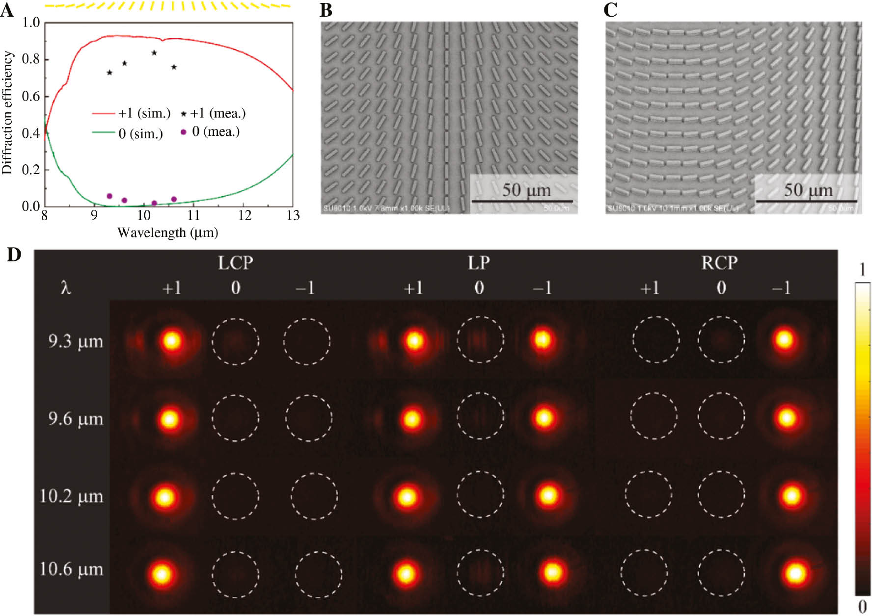
Experimental results of the beam deflector.
(A) Simulated (red and green lines) and measured (black stars and purple dots) diffraction efficiencies of the deflector under LCP illumination. (B, C) SEM images of the fabricated sample. (D) Measured reflected patterns produced by the deflector at different wavelengths under LCP, LP, and RCP illuminations.
To experimentally verify the performance of the beam deflector, a sample with the area of 1×1 cm2 is fabricated; the scanning electron microscope (SEM) images are illustrated in Figure 3B and C. The fabrication method and tolerance analysis, as well as the measurement method, are given in sections S4 and S5, Supplementary Material. The measured reflection patterns at several wavelengths ranging from 9.3 to 10.6 μm (available wavelength range of our laser) are shown in Figure 3D. The central dim spot (0th order) is attributed to the unmodulated spin component of reflected beam, while +1st- and −1st-order bright spots stem from the anomalous reflection of two converted spin components. One can see that the main energy is diffracted to the desired orders. The left panel shows the results at the wavelengths of 9.3 μm, 9.6 μm, 10.2 μm, and 10.6 μm under LCP light incidence; the measured efficiencies of the +1st-order diffractions are 72.8%, 77.9%, 83.6%, and 75.9%, respectively. The results are added in Figure 3A (black stars and purple dots) for comparison with the simulated results, where the slight discrepancy between them is attributed to the imperfection of fabrication and measurement errors. The diffraction patterns under linearly polarized (LP) and RCP illuminations are also measured as depicted in the middle and right panels in Figure 3D.
A phase-only meta-hologram is also designed to further demonstrate the high performance of the all-metallic configuration. The phase map of the holographic image is computed, a Chinese Tai Ji diagram, by means of the point-source algorithm. Then the hologram is coded via rotating the metal bricks according to the Φ-φ relation. A sample with the area of 2×2 cm2 (2500×2500 pixels) is fabricated. Figure 4A and B display the theoretically calculated and experimentally measured holographic patterns, respectively. Clearly, the measured result agrees well with the calculated one, which demonstrates the extremely high fidelity of the meta-hologram. The SEM images of the fabricated sample are shown in Figure 4C and D.

Experimental results of the hologram.
(A) Theoretically calculated and (B) measured holographic images under LCP illumination at the wavelength of 10.6 μm. The measured efficiency is ~77%. (C, D) SEM images of the fabricated sample.
4 Conclusion
In summary, we have demonstrated a kind of all-metallic GMs which can achieve broadband and high-efficiency phase control in the reflection mode. Two metadevices are experimentally characterized in the infrared band, whose performances agree well with the numerical designs. This design method is universal and can be easily scaled to any other spectra. We believe that this high-performance approach could find potential in various practical applications such as beam steering and holographic display. In addition, it is noteworthy that all-metallic structures in general have excellent mechanical and physical properties such as high strength, large flexibility, and good ductility, which are significant in practical engineering.
See Supplementary Material for the supporting content.
Funding source: National Natural Science Foundation of China
Award Identifier / Grant number: 61575201
Award Identifier / Grant number: 61622508
Award Identifier / Grant number: 61822511
Funding statement: The authors declare no competing financial interest. This work is supported by the National Natural Science Foundation of China under Grant Nos. 61575201, 61622508, and 61822511, Funder Id: http://dx.doi.org/10.13039/501100001809.
References
[1] Lin D, Fan P, Hasman E, Brongersma ML. Dielectric gradient metasurface optical elements. Science 2014;345:298–302.10.1126/science.1253213Search in Google Scholar PubMed
[2] Yu N, Capasso F. Flat optics with designer metasurfaces. Nat Mater 2014;13:139.10.1038/nmat3839Search in Google Scholar PubMed
[3] Pu M, Guo Y, Ma X, Li X, Luo X. Methodologies for on-demand dispersion engineering of waves in metasurfaces. Adv Opt Mater 2019;7:1801376.10.1002/adom.201801376Search in Google Scholar
[4] Luo X. Subwavelength artificial structures: opening a new era for engineering optics. Adv Mater 2019;31:1804680.10.1002/adma.201804680Search in Google Scholar PubMed
[5] Nemati A, Wang Q, Hong M, Teng J. Tunable and reconfigurable metasurfaces and metadevices. Opto-Electron Adv 2018;1:180009.10.29026/oea.2018.180009Search in Google Scholar
[6] Litchinitser NM. Photonic multitasking enabled with geometric phase. Science 2016;352:1177–8.10.1126/science.aaf8391Search in Google Scholar PubMed
[7] Li Z, Kim I, Zhang L, et al. Dielectric meta-holograms enabled with dual magnetic resonances in visible light. ACS Nano 2017;11:9382–9.10.1021/acsnano.7b04868Search in Google Scholar PubMed
[8] Sun S, Yang KY, Wang CM, et al. High-efficiency broadband anomalous reflection by gradient meta-surfaces. Nano Lett 2012;12:6223–9.10.1021/nl3032668Search in Google Scholar PubMed
[9] Jing L, Wang Z, Maturi R, et al. Gradient chiral metamirrors for spin-selective anomalous reflection. Laser Photonics Rev 2017;11:1700115.10.1002/lpor.201700115Search in Google Scholar
[10] Pu M, Li X, Ma X, et al. Catenary optics for achromatic generation of perfect optical angular momentum. Sci Adv 2015;1:e1500396.10.1126/sciadv.1500396Search in Google Scholar PubMed PubMed Central
[11] Zeng J, Li L, Yang X, Gao J. Generating and separating twisted light by gradient-rotation split-ring antenna metasurfaces. Nano Lett 2016;16:3101–8.10.1021/acs.nanolett.6b00360Search in Google Scholar PubMed
[12] Wang S, Wu PC, Su VC, et al. Broadband achromatic optical metasurface devices. Nat Commun 2017;8:187.10.1038/s41467-017-00166-7Search in Google Scholar PubMed PubMed Central
[13] Li X, Chen L, Li Y, et al. Multicolor 3D meta-holography by broadband plasmonic modulation. Sci Adv 2016;2:e1601102.10.1126/sciadv.1601102Search in Google Scholar PubMed PubMed Central
[14] Wang B, Dong F, Li QT, et al. Visible-frequency dielectric metasurfaces for multiwavelength achromatic and highly dispersive holograms. Nano Lett 2016;16:5235–40.10.1021/acs.nanolett.6b02326Search in Google Scholar PubMed
[15] Huang L, Chen X, Mühlenbernd H, et al. Three-dimensional optical holography using a plasmonic metasurface. Nat Commun 2013;4:2808.10.1038/ncomms3808Search in Google Scholar
[16] Niv A, Gorodetski Y, Kleiner V, Hasman E. Topological spin-orbit interaction of light in anisotropic inhomogeneous subwavelength structures. Opt Lett 2008;33:2910–2.10.1364/OL.33.002910Search in Google Scholar PubMed
[17] Bliokh KY, Rodríguez-Fortuño FJ, Nori F, Zayats AV. Spin-orbit interactions of light. Nat Photonics 2015;9:796.10.1038/nphoton.2015.201Search in Google Scholar
[18] Ding X, Monticone F, Zhang K, et al. Ultrathin Pancharatnam-Berry metasurface with maximal cross-polarization efficiency. Adv Mater 2015;27:1195–200.10.1002/adma.201405047Search in Google Scholar PubMed
[19] Qin F, Ding L, Zhang L, et al. Hybrid bilayer plasmonic metasurface efficiently manipulates visible light. Sci Adv 2016;2:e1501168.10.1126/sciadv.1501168Search in Google Scholar PubMed PubMed Central
[20] Khorasaninejad M, Chen WT, Devlin RC, Oh J, Zhu AY, Capasso F. Metalenses at visible wavelengths: diffraction-limited focusing and subwavelength resolution imaging. Science 2016;352:1190–4.10.1126/science.aaf6644Search in Google Scholar PubMed
[21] Devlin RC, Khorasaninejad M, Chen WT, Oh J, Capasso F. Broadband high-efficiency dielectric metasurfaces for the visible spectrum. Proc Natl Acad Sci 2016;113:10473–8.10.1073/pnas.1611740113Search in Google Scholar PubMed PubMed Central
[22] Chen BH, Wu PC, Su VC, et al. GaN metalens for pixel-level full-color routing at visible light. Nano Lett 2017;17:6345–52.10.1021/acs.nanolett.7b03135Search in Google Scholar PubMed
[23] Wang S, Wu PC, Su VC, et al. A broadband achromatic metalens in the visible. Nat Nanotechnol 2018;13:227.10.1038/s41565-017-0052-4Search in Google Scholar PubMed
[24] Yan C, Li X, Pu M, et al. Midinfrared real-time polarization imaging with all-dielectric metasurfaces. Appl Phys Lett 2019;114:161904.10.1063/1.5091475Search in Google Scholar
[25] Pors A, Nielsen MG, Bozhevolnyi SI. Broadband plasmonic half-wave plates in reflection. Opt Lett 2013;38:513–5.10.1364/OL.38.000513Search in Google Scholar PubMed
[26] Zheng G, Mühlenbernd H, Kenney M, Li G, Zentgraf T, Zhang S. Metasurface holograms reaching 80% efficiency. Nat Nanotechnol 2015;10:308.10.1038/nnano.2015.2Search in Google Scholar PubMed
[27] Wen D, Yue F, Li G, et al. Helicity multiplexed broadband metasurface holograms. Nat Commun 2015;6:8241.10.1038/ncomms9241Search in Google Scholar PubMed PubMed Central
[28] Chen WT, Yang KY, Wang CM, et al. High-efficiency broadband meta-hologram with polarization-controlled dual images. Nano Lett 2013;14:225–30.10.1021/nl403811dSearch in Google Scholar PubMed
[29] Huang YW, Chen WT, Tsai WY, et al. Aluminum plasmonic multicolor meta-hologram. Nano Lett 2015;15:3122–7.10.1021/acs.nanolett.5b00184Search in Google Scholar PubMed
[30] Xie X, Li X, Pu M, et al. Plasmonic metasurfaces for simultaneous thermal infrared invisibility and holographic illusion. Adv Funct Mater 2018;28:1706673.10.1002/adfm.201706673Search in Google Scholar
[31] Xie X, Pu M, Liu K, et al. High-efficiency and tunable circular-polarization beam splitting with a liquid-filled all-metallic catenary meta-mirror. Adv Mater Technol 2019;4:1900334.10.1002/admt.201900334Search in Google Scholar
[32] Pu M, Ma XL, Guo Y, Li X, Luo X. Theory of microscopic meta-surface waves based on catenary optical fields and dispersion. Opt Express 2018;26:19555–62.10.1364/OE.26.019555Search in Google Scholar PubMed
[33] Xie X, Pu M, Huang Y, et al. Heat resisting metallic meta-skin for simultaneous microwave broadband scattering and infrared invisibility based on catenary optical field. Adv Mater Technol 2019;4:1800612.10.1002/admt.201800612Search in Google Scholar
[34] Feng Q, Pu M, Hu C, Luo X. Engineering the dispersion of metamaterial surface for broadband infrared absorption. Opt Lett 2012;37:2133–5.10.1364/OL.37.002133Search in Google Scholar PubMed
Supplementary Material
The online version of this article offers supplementary material (https://doi.org/10.1515/nanoph-2019-0415).
© 2019 Xiangang Luo et al., published by De Gruyter, Berlin/Boston
This work is licensed under the Creative Commons Attribution 4.0 International License.
Articles in the same Issue
- Editorial
- Editorial on special issue “Metamaterials and Plasmonics in Asia”
- Reviews
- Metamaterials – from fundamentals and MEMS tuning mechanisms to applications
- Large-area metasurface on CMOS-compatible fabrication platform: driving flat optics from lab to fab
- Tip-enhanced photoluminescence nano-spectroscopy and nano-imaging
- Plasmon-enhanced organic and perovskite solar cells with metal nanoparticles
- Plasmonic nanostructures in photodetection, energy conversion and beyond
- Broadband metamaterials and metasurfaces: a review from the perspectives of materials and devices
- Visible to long-wave infrared chip-scale spectrometers based on photodetectors with tailored responsivities and multispectral filters
- Research Articles
- All-metallic geometric metasurfaces for broadband and high-efficiency wavefront manipulation
- Revealing photonic Lorentz force as the microscopic origin of topological photonic states
- Topological edge and corner states in a two-dimensional photonic Su-Schrieffer-Heeger lattice
- Dual-band dichroic asymmetric transmission of linearly polarized waves in terahertz chiral metamaterial
- A conformal transformation approach to wide-angle illusion device and absorber
- A complete phase diagram for dark-bright coupled plasmonic systems: applicability of Fano’s formula
- Optical telescope with Cassegrain metasurfaces
- Smart sensing metasurface with self-defined functions in dual polarizations
- Experimental nanofocusing of surface plasmon polaritons using a gravitational field
- Mechanotunable optical filters based on stretchable silicon nanowire arrays
- Extraordinary optical transmission and second harmonic generation in sub–10-nm plasmonic coaxial aperture
- Particle simulation of plasmons
- AI-assisted on-chip nanophotonic convolver based on silicon metasurface
- Hybrid organic-inorganic perovskite metamaterial for light trapping and photon-to-electron conversion
- Proposed method for highly selective resonant optical manipulation using counter-propagating light waves
- Temperature-dependent dark-field scattering of single plasmonic nanocavity
- On-chip trans-dimensional plasmonic router
- Chaotic photon spheres in non-Euclidean billiard
- Systematic studies for improving device performance of quantum well infrared stripe photodetectors
- Wide gamut, angle-insensitive structural colors based on deep-subwavelength bilayer media
- Generation of terahertz vector beams using dielectric metasurfaces via spin-decoupled phase control
- Loss and gain in a plasmonic nanolaser
- Flexibly tunable surface plasmon resonance by strong mode coupling using a random metal nanohemisphere on mirror
- Dynamic tuning of enhanced intrinsic circular dichroism in plasmonic stereo-metamolecule array with surface lattice resonance
- Directing Cherenkov photons with spatial nonlocality
- Narrow-frequency sharp-angular filters using all-dielectric cascaded meta-gratings
- Reconfigurable topological waveguide based on honeycomb lattice of dielectric cuboids
- Optical spin-dependent beam separation in cyclic group symmetric metasurface
- Helicity-delinked manipulations on surface waves and propagating waves by metasurfaces