Reconfigurable topological waveguide based on honeycomb lattice of dielectric cuboids
-
Xing-Xiang Wang
 and
Xiao Hu
and
Xiao Hu


Abstract
We show that the photonic crystal (PhC) made of dielectric cuboids with their centers forming a honeycomb lattice is characterized by a
1 Introduction
The discovery of quantum Hall effect (QHE) opened a new chapter of condensed matter physics and related materials science [1]. QHE occurs in a two-dimensional (2D) electron gas where electric current flows along the edge without dissipation. The novel quantum state was found to emerge from the topology of band structure [2]. In the past two decades, other topological states such as quantum anomalous Hall effect (QAHE) and quantum spin Hall effect (QSHE) have also been found [3], [4], [5], [6], [7], [8], [9]. Potential applications of topological quantum states such as quantum computation were proposed as well [10]. However, electronic materials with non-trivial topology are difficult to prepare, and only work at very low temperatures up to the moment of writing, which hinder them from applications at present stage.
In 2005, Haldane and Raghu revealed that by using gyrotropic materials with Faraday effect topological states can be achieved in photonic crystals (PhCs) [11], which are structures with periodic arrangements of dielectric permittivity and/or magnetic permeability, and are much easier to fabricate as compared to electronic materials. In recent years, topological states have been demonstrated in many photonic systems at room temperature [12], [13], [14], [15], [16], [17], [18], [19], [20], [21], [22], [23], [24], [25], [26], [27], [28], [29], [30], [31], [32].
In this article, we focus on topological photonic crystals based on dielectric materials. We start from the discussion on the symmetries of honeycomb lattice which guarantee the Dirac cones. We then show how to achieve a topological PhC and a trivial PhC in honeycomb structure by using dielectric cuboids. These two PhCs can be converted to each other by rotating the cuboids. We discuss that a photonic circuit board hosting reconfigurable topological waveguide can be designed which may be useful for future photonic devices.
2 Tight-binding analysis
We consider a tight-binding (TB) Hamiltonian defined on honeycomb lattice, and choose the hexagonal unit cell which contains six sites
where t0, t1 > 0 represent the nearest-neighbor (NN) hopping integrals inside and between the hexagonal unit cells (see Figure 1a) [33], [34].

(a) Schematic plot of a honeycomb lattice with the unit cell represented by the black dashed hexagon. Each unit cell contains six lattice sites which are numbered from 1 to 6. The blue and red bonds stand for t0 and t1, which are the nearest-neighbor hoppings inside and between the hexagonal unit cells, respectively, and the green bonds stand for t2, the coupling between next-next-nearest sites inside the unit cell. (b) Schematic plot of the unit cell after the C3 operation which rotates the lattice around site 1 by 2π/3 clockwise, whereby 1 → 1′, 2 → 2′, …, 6 → 6′. The C3 operation does not affect site 1, 3 and 5 considering periodicity of the lattice, but rotates the order of 2, 4 and 6.
Let us first consider the case of uniform hopping t0 = t1, with the dispersion and the first Brillouin zone shown in Figure 2a and b, respectively. In this case, two symmetries are important. The first symmetry is the C6v symmetry of the unit cell, and the second one is the C3 rotational symmetry from C3v point group with regard to the lattice sites, which guarantee the four-fold degeneracy at
as shown in Figure 1b. The eigenstates of Hamiltonian at

(a) Band structure for conventional honeycomb lattice. (b) The first Brillouin zone, where
Transforming the
It is clear that the two modes
In order to break the C3 symmetry and thus open an energy gap, one can take t0 ≠ t1 in Hamiltonian (1) (see Figure 1a) [20], [33]. Alternatively, one can introduce the interaction between the next-next-nearest (NNN) sites
additionally with t2 > 0 inside a unit cell which is marked by the green bonds in Figure 1a.
Taking t0 as the unit of energy, we numerically calculate the band structure for typical values of t1 and t2. As shown in Figure 2c for t1 = t0 and t2 = 0.1t0, the four-fold degeneracy is split into two pairs of doubly degenerate modes corresponding to the 2D representations of C6v point group. In contrast to the case t1 > t0 (and t2 = 0) discussed in previous works [20], [33], the second and third bands are separated from the others in the whole Brillouin zone in the present case, which makes the characterization of band topology based on Wilson-loop spectra possible. As shown in Figure 2d, the two eigenvalues of Wilson-loop phases wind between −π and π, which indicates a topological phase characterized by
In order to see the energies of p modes and d modes, we notice
As shown in Figure 2e for t1 = 1.16t0 and t2 = 0.1t0, the bandgap becomes larger than the one in Figure 2c without change in topology according to the Wilson-loop spectrum (Figure 2f), which shows the same winding as the spectrum in Figure 2d.
As shown in Figure 2g, there is also a bandgap for t1 = 0.86t0 and t2 = 0. The configuration of C2 eigenvalues is balanced between
To end this part, we notice that it is also possible to achieve topological state even for t1 < t0, where an even larger value of t2 is required as shown in Figure 2i, j.
3 Topological PhC with dielectric cuboids
Based on the above discussion, one can open a bandgap by replacing the cylinders discussed in the previous work [20] with cuboids in the honeycomb PhC which breaks the C3 symmetry. As shown in Figure 3, there are two possible arrangements preserving the C6v symmetry, which are called circular and radial structures in the present work.

Schematic plot of (a) the circular structure and (b) the radial structure. a1 and a2 are unit vectors with length a0 which is the lattice constant. In both structures, R = a0/3 since the centers of cuboids are placed at the honeycomb lattice sites.
Electromagnetic (EM) waves in a dielectric PhC are described by Maxwell’s equations
with constitution relationships
where ε and μ = μ0 are position-dependent permittivity and constant permeability, respectively.
For simplicity the PhC is assumed infinitely tall along z direction. We focus on the TM modes which contains only out-of-plane electric field Ez and in-plane magnetic field Hx and Hy. The master equation for the harmonic modes of frequency ω can be obtained from Maxwell’s Equations (6)
where ε(r) is the position-dependent relative permittivity,
We solve the master equation (8) using the finite-element-analysis (FEA) software COMSOL Multiphysics® [37]. The photonic band structures are obtained with periodic boundary conditions imposed along both a1 and a2 given in Figure 3. The eigenstates at

(a) Distributions of
In the circular structure, it is clear that t0 > t1 and
The radial structure corresponds to a case t0 < t1 and t2 > 0 as can be read from the lattice structure, whereas the next-nearest site interactions (such as coupling between site 1 and site 3 in Figure 1a) are small and can be neglected. As displayed in the right panel of Figure 4c, at M point, the lower (higher) bands are still occupied by
Comparing results based on TB model and Maxwell’s equations provides useful insights in investigation of photonic topology. In the present design, the NNN site interaction is enhanced in the topological photonic crystal where cuboids are pointing to the center of the unit cell, and the resultant photonic band configuration at K point is consistent with the discussion based on the TB model. Nevertheless, the photonic band structure obtained by numerical analysis of Maxwell’s equation is not easy to be reproduced by a simple TB model with a small set of parameters.
According to the bulk-edge correspondence for band topology, topological interface modes should appear at the interface between PhCs of the radial and circular structures. In order to see this explicitly, we consider a ribbon structure shown in Figure 5a with the dispersion relation displayed in Figure 5b. One can see two additional bands inside the bulk bandgap associated with the topological interface modes, which penetrate into the continuum of bulk bands with small anti-crossings. There is a tiny gap at kx = 0 in Figure 5b due to the broken C6v symmetry at the armchair-type interface [34], which, however, is unnoticeable in the present scale. We checked a pair of opposite momenta on the interface bands with the same frequency (dots in red and blue colors in Figure 5b). As can be seen in Figure 5c, the mode marked in red (blue) dot shows counterclockwise (clockwise) rotating Poynting vectors, which indicates a pseudospin-up (pseudospin-down) mode. Taking average of the local Poynting vectors over the hexagonal unit cell, the EM energy flow of the mode marked in red (blue) dot is towards left (right). Therefore, the propagation directions for up and down pseudospins are opposite, which corresponds to the pseudospin-momentum locking feature similar to QSHE.
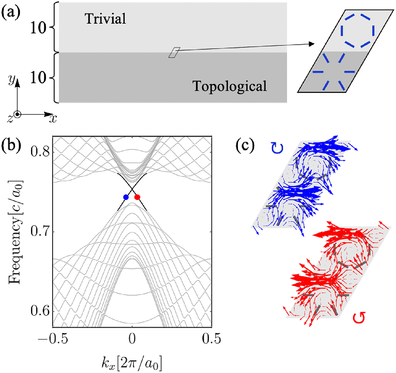
(a) Schematic plot of a ribbon structure infinitely long in x direction and periodic in y direction with width of 20 unit cells. (b) Band structure for the ribbon in (a). Gray and black lines represent bulk modes and topological interface modes. (c) Distributions of local Poynting vector in unit cells on the two sides of the interface for the modes marked in blue and red dots in (b).
We also simulated the propagation of EM wave excited by a source in real space. In Figure 6a, the EM wave is excited by a linearly polarized source

Real-space simulations of the EM transportation along the topological interface. (a), (b) and (c) Interface modes excited by a linearly polarized source, a pseudospin-down source, and a pseudospin-up source, respectively. (d) Robust interface transportation along the interface including a sharp corner. The panels contain 37 ℒ 20 unit cells.
We notice that the radial and circular structures are related to each other by rotating the six cuboids in a unit cell around their own centers (see Figure 7a). As shown in Figure 7b, the topological frequency bandgap decreases gradually when θ increases from 0 and closes at
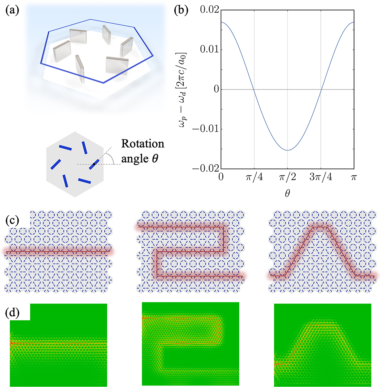
(a) Schematic plot of a unit cell with rotation angle θ. (b) Difference between frequencies of p and d modes. (c) Schematic plots of typical configurations of topological waveguide. (d) Real-space simulation results for (c). The panels in (d) contain 40 × 40 unit cells.
Because of the above property, one can fabricate a photonic circuit board as shown in Figure 7c schematically, where the topological waveguide can be rewritten by merely rotating individual cuboids. As can be seen in Figure 7d obtained by real-space simulations, the EM wave propagates along the designed topological waveguides.
4 Conclusions
In conclusion, we show that in honeycomb lattice the C3 symmetry from C3v point group around the lattice sites and the C6v symmetry around the center of the hexagonal unit cell guarantee a four-fold degeneracy and double Dirac cone at
Funding source: Core Research for Evolutional Science and Technology, Japan Science and Technology Agency
Award Identifier / Grant number: JPMJCR18T4
Funding source: Grants-in-Aid for Scientific Research, Japan Society for the Promotion of Science
Award Identifier / Grant number: 17H02913
Acknowledgment
The authors thank R. Yu and Y.-C. Jiang for useful discussions about Wilson-loop spectra.
Author contribution: All the authors have accepted responsibility for the entire content of this submitted manuscript and approved submission.
Research funding: This research was funded by the CREST, JST (Core Research for Evolutionary Science and Technology, Japan Science and Technology Agency) (Grant Number JPMJCR18T4), and partially by the Grants-in-Aid for Scientific Research No. 17H02913, JSPS (Japan Society of Promotion of Science).
Conflict of interest statement: The authors declare no conflicts of interest regarding this article.
References
[1] K. V. Klitzing, G. Dorda, and M. Pepper, “New method for highaccuracy determination of the fine-structure constant based on quantized hall resistance,” Phys. Rev. Lett., vol. 45, no. 6, pp. 494–497, 1980, https://doi.org/10.1103/PhysRevLett.45.494.Search in Google Scholar
[2] D. J. Thouless, M. Kohmoto, M. P. Nightingale, and M. Nijs, “Quantized Hall conductance in a two-dimensional periodic potential,” Phys. Rev. Lett., vol. 49, no. 6, pp. 405–408, 1982, https://doi.org/10.1103/PhysRevLett.49.405.Search in Google Scholar
[3] F. D. M. Haldane, “Model for a quantum Hall effect without landau levels: condensed-matter realization of the ‘parity anomaly’,” Phys. Rev. Lett., vol. 61, no. 18, pp. 2015–2018, 1988, https://doi.org/10.1103/PhysRevLett.61.2015.Search in Google Scholar
[4] H. Weng, R. Yu, X. Hu, X. Dai, and Z. Fang, “Quantum anomalous Hall Effect and related topological electronic states,” Adv. Phys., vol. 64, no. 3, pp. 227–282, 2015, https://doi.org/10.1080/00018732.2015.1068524.Search in Google Scholar
[5] C. L. Kane, and E. J. Mele, “Quantum spin Hall effect in graphene,” Phys. Rev. Lett., vol. 95, no. 22, 2005, Art no. 226801, https://doi.org/10.1103/PhysRevLett.95.226801.Search in Google Scholar
[6] B. A. Bernevig, T. L. Hughes, and S.-C. Zhang, “Quantum spin Hall effect and topological phase transition in HgTe quantum wells,” Science, vol. 314, no. 5806, pp. 1757–1761, 2006, https://doi.org/10.1126/science.1133734.Search in Google Scholar
[7] D. Xiao, M. C. Chang, and Q. Niu, “Berry phase Effects on electronic properties,” Rev. Mod. Phys., vol. 82, no. 3, pp. 1959–2007, 2010, https://doi.org/10.1103/RevModPhys.82.1959.Search in Google Scholar
[8] M. Z. Hasan, and C. L. Kane, “Colloquium: Topological insulators,” Rev. Mod. Phys., vol. 82, no. 4, pp. 3045–3067, 2010, https://doi.org/10.1103/RevModPhys.82.30.Search in Google Scholar
[9] X.-L. Qi, and S.-C. Zhang, “Topological insulators and superconductors,” Rev. Mod. Phys., vol. 83, no. 4, pp. 1057–1110, 2011, https://doi.org/10.1103/RevModPhys.83.1057.Search in Google Scholar
[10] C. Nayak, S. H. Simon, A. Stern, M. Freedman, and S. Das Sarma, “Non-Abelian anyons and topological quantum computation,” Rev. Mod. Phys., vol. 80, no. 3, pp. 1083–1159, 2008, https://doi.org/10.1103/RevModPhys.80.1083.Search in Google Scholar
[11] F. D. M. Haldane and S. Raghu, “Possible realization of directional optical waveguides in photonic crystals with broken time-reversal symmetry,” Phys. Rev. Lett., vol. 100, no. 1, 2008, Art no. 013904, https://doi.org/10.1103/PhysRevLett.100.013904.Search in Google Scholar
[12] Z. Wang, Y. D. Chong, J. D. Joannopoulos, and M. Soljačić, “Reection-free one-way edge modes in a gyromagnetic photonic crystal,” Phys. Rev. Lett., vol. 100, no. 1, 2008, Art no. 013905, https://doi.org/10.1103/PhysRevLett.100.013905.Search in Google Scholar
[13] S. Raghu, and F. D. M. Haldane, “Analogs of quantum-Halleffect edge states in photonic crystals,” Phys. Rev. A, vol. 78, no. 3, 2008, Art no. 033834, https://doi.org/10.1103/PhysRevA.78.033834.Search in Google Scholar
[14] Z. Wang, Y. Chong, J. D. Joannopoulos, and M. Soljačić, “Observation of unidirectional backscattering-immune topological electromagnetic states,” Nature, vol. 461, no. 7265, pp. 772–775, 2009, https://doi.org/10.1038/nature08293.Search in Google Scholar
[15] M. Hafezi, E. A. Demler, M. D. Lukin, and J. M. Taylor, “Robust optical delay lines with topological protection,” Nat. Phys., vol. 7, no. 11, pp. 907–912, 2011, https://doi.org/10.1038/nphys2063.Search in Google Scholar
[16] M. Hafezi, S. Mittal, J. Fan, A. Migdall, and J. M. Taylor, “Imaging topological edge states in silicon photonics,” Nat. Photonics, vol. 7, no. 12, pp. 1001–1005, 2013, https://doi.org/10.1038/nphoton.2013.274.Search in Google Scholar
[17] A. B. Khanikaev, S. Hossein Mousavi, W. K. Tse, M. Kargarian, A. H. MacDonald, and G. Shvets, “Photonic topological insulators,” Nat. Mater., vol. 12, no. 3, pp. 233–239, 2013, https://doi.org/10.1038/nmat3520.Search in Google Scholar
[18] M. C. Rechtsman, J. M. Zeuner, Y. Plotnik, et al., “Photonic Floquet topological insulators,” Nature, vol. 496, no. 7444, pp. 196–200, 2013, https://doi.org/10.1038/nature12066.Search in Google Scholar
[19] L. Lu, J. D. Joannopoulos, and M. Soljačić, “Topological photonics,” Nat. Photonics, vol. 8, no. 11, pp. 821–829, 2014, https://doi.org/10.1038/nphoton.2014.248.Search in Google Scholar
[20] L.-H. Wu and X. Hu, “Scheme for achieving a topological photonic crystal by using dielectric material,” Phys. Rev. Lett., vol. 114, no. 22, 2015, Art no. 223901, https://doi.org/10.1103/PhysRevLett.114.223901.Search in Google Scholar
[21] S. Barik, H. Miyake, W. DeGottardi, E. Waks and M. Hafezi, “Two-dimensionally confined topological edge states in photonic crystals,” New J. Phys., vol. 18, no. 11, 2016, Art no. 113013, https://doi.org/10.1088/1367-2630/18/11/113013.Search in Google Scholar
[22] A. B. Khanikaev and G. Shvets, “Two-dimensional topological photonics,” Nat. Photonics, vol. 11, no. 12, pp. 763–773, 2017, https://doi.org/10.1038/s41566-017-0048-5.Search in Google Scholar
[23] G. Siroki, P. A. Huidobro and V. Giannini, “Topological photonics: from crystals to particles,” Phys. Rev. B, vol. 96, no. 4, 2017, Art no. 041408, https://doi.org/10.1103/PhysRevB.96.041408.Search in Google Scholar
[24] B. Bahari, A. Ndao, F. Vallini, A. El Amili, Y. Fainman and B. Kanté, “Nonreciprocal lasing in topological cavities of arbitrary geometries,” Science, vol. 358, no. 6363, pp. 636–640, 2017, https://doi.org/10.1126/science.aao4551.Search in Google Scholar
[25] Y. Yang, Y. F. Xu, T. Xu, et al., “Visualization of a unidirectional electromagnetic waveguide using topological photonic crystals made of dielectric materials,” Phys. Rev. Lett., vol. 120, no. 21, 2018, Art no. 217401, https://doi.org/10.1103/PhysRevLett.120.217401.Search in Google Scholar
[26] Y. Yang, H. Jiang and Z. H. Hang, “Topological valley transport in two-dimensional honeycomb photonic crystals,” Sci. Rep., vol. 8, no. 1, pp. 1588, 2018, https://doi.org/10.1038/s41598-018-20001-3.Search in Google Scholar
[27] S. Barik, A. Karasahin, C. Flower, et al., “A topological quantum optics interface,” Science, vol. 359, no. 6376, pp. 666–668, 2018, https://doi.org/10.1126/science.aaq0327.Search in Google Scholar
[28] G. Harari, M. A. Bandres, Y. Lumer, et al., “Topological insulator laser: theory,” Science, vol. 359, no. 6381, 2018, Art no. eaar4003, https://doi.org/10.1126/science.aar4003.Search in Google Scholar
[29] M. A. Bandres, S. Wittek, G. Harari, et al., “Topological insulator laser: experiments,” Science, vol. 359, no. 6381, 2018, Art no. eaar4005, https://doi.org/10.1126/science.aar4005.Search in Google Scholar
[30] T. Ozawa, H. M. Price, A. Amo, et al., “Topological photonics,” Rev. Mod. Phys., vol. 91, no. 1, 2019, Art no. 15006, https://doi.org/10.1103/RevModPhys.91.015006.Search in Google Scholar
[31] S. Peng, N. J. Schilder, X. Ni, et al., “Probing the band structure of topological silicon photonic lattices in the visible spectrum,” Phys. Rev. Lett., vol. 122, no. 11, 2019, Art no. 117401, https://doi.org/10.1103/PhysRevLett.122.117401.Search in Google Scholar
[32] Z.-K. Shao, H.-Z. Chen, S. Wang, et al., “A high-performance topological bulk laser based on band-inversion-induced reection,” Nat. Nanotechnol., vol. 15, no. 1, pp. 67–72, 2020, https://doi.org/10.1038/s41565-019-0584-x.Search in Google Scholar
[33] L.-H. Wu and X. Hu, “Topological properties of electrons in honeycomb lattice with detuned hopping energy,” Sci. Rep., vol. 6, no. 1, 2016, Art no. 24347, https://doi.org/10.1038/srep24347.Search in Google Scholar
[34] T. Kariyado and X. Hu, “Topological states characterized by mirror winding numbers in graphene with bond modulation,” Sci. Rep., vol. 7, no. 1, 2017, Art no. 16515, https://doi.org/10.1038/s41598-017-16334-0.Search in Google Scholar
[35] M. Dresselhaus, G. Dresselhaus and A. Jorio. Group Theory Application to the Physics of Condensed Matter, Springer-Verlag Berlin Heidelberg, 2008.Search in Google Scholar
[36] M. B. de Paz, M. G. Vergniory, D. Bercioux, A. García-Etxarri and B. Bradlyn, “Engineering fragile topology in photonic crystals: topological quantum chemistry of light,” Phys. Rev. Res., vol. 1, no. 3, 2019, Art no. 032005, https://doi.org/10.1103/PhysRevResearch.1.032005.Search in Google Scholar
[37] COMSOL Multiphysics®v. 5.4. Stockholm, Sweden: COMSOL AB; 2018. www.comsol.com.Search in Google Scholar
© 2020 Xing-Xiang Wang and Xiao Hu, published by De Gruyter, Berlin/Boston
This work is licensed under the Creative Commons Attribution 4.0 International License.
Articles in the same Issue
- Editorial
- Editorial on special issue “Metamaterials and Plasmonics in Asia”
- Reviews
- Metamaterials – from fundamentals and MEMS tuning mechanisms to applications
- Large-area metasurface on CMOS-compatible fabrication platform: driving flat optics from lab to fab
- Tip-enhanced photoluminescence nano-spectroscopy and nano-imaging
- Plasmon-enhanced organic and perovskite solar cells with metal nanoparticles
- Plasmonic nanostructures in photodetection, energy conversion and beyond
- Broadband metamaterials and metasurfaces: a review from the perspectives of materials and devices
- Visible to long-wave infrared chip-scale spectrometers based on photodetectors with tailored responsivities and multispectral filters
- Research Articles
- All-metallic geometric metasurfaces for broadband and high-efficiency wavefront manipulation
- Revealing photonic Lorentz force as the microscopic origin of topological photonic states
- Topological edge and corner states in a two-dimensional photonic Su-Schrieffer-Heeger lattice
- Dual-band dichroic asymmetric transmission of linearly polarized waves in terahertz chiral metamaterial
- A conformal transformation approach to wide-angle illusion device and absorber
- A complete phase diagram for dark-bright coupled plasmonic systems: applicability of Fano’s formula
- Optical telescope with Cassegrain metasurfaces
- Smart sensing metasurface with self-defined functions in dual polarizations
- Experimental nanofocusing of surface plasmon polaritons using a gravitational field
- Mechanotunable optical filters based on stretchable silicon nanowire arrays
- Extraordinary optical transmission and second harmonic generation in sub–10-nm plasmonic coaxial aperture
- Particle simulation of plasmons
- AI-assisted on-chip nanophotonic convolver based on silicon metasurface
- Hybrid organic-inorganic perovskite metamaterial for light trapping and photon-to-electron conversion
- Proposed method for highly selective resonant optical manipulation using counter-propagating light waves
- Temperature-dependent dark-field scattering of single plasmonic nanocavity
- On-chip trans-dimensional plasmonic router
- Chaotic photon spheres in non-Euclidean billiard
- Systematic studies for improving device performance of quantum well infrared stripe photodetectors
- Wide gamut, angle-insensitive structural colors based on deep-subwavelength bilayer media
- Generation of terahertz vector beams using dielectric metasurfaces via spin-decoupled phase control
- Loss and gain in a plasmonic nanolaser
- Flexibly tunable surface plasmon resonance by strong mode coupling using a random metal nanohemisphere on mirror
- Dynamic tuning of enhanced intrinsic circular dichroism in plasmonic stereo-metamolecule array with surface lattice resonance
- Directing Cherenkov photons with spatial nonlocality
- Narrow-frequency sharp-angular filters using all-dielectric cascaded meta-gratings
- Reconfigurable topological waveguide based on honeycomb lattice of dielectric cuboids
- Optical spin-dependent beam separation in cyclic group symmetric metasurface
- Helicity-delinked manipulations on surface waves and propagating waves by metasurfaces