Design of a compact UWB antenna with a partial ground plane on epoxy woven glass material
-
Md. Moinul Islam
 ,
Mohammad Tariqul Islam
,
Mohammad Tariqul Islam

Abstract
A compact ultra-wideband (UWB) antenna is presented in this paper with a partial ground plane on epoxy woven glass material. The study is discussed to comprehend the effects of various design parameters with explicit parametric analyses. The overall antenna dimension is 0.22×0.26×0.016 λ. A prototype is made on epoxide woven glass fabric dielectric material of 1.6 mm thickness. The measured results point out that the reported antenna belongs to a wide bandwidth comprehending from 3 GHz to more than 11 GHz with VSWR<2. It has a peak gain of 5.52 dBi, where 3.98 dBi is the average gain. Nearly omnidirectional radiation patterns are observed within the operating frequency bands. A good term exists between simulation and measurement results, which lead the reported antenna to be an appropriate candidate for UWB applications.
1 Introduction
Ultra-wideband (UWB) technology has nowadays been used in short-distance wireless communication systems thoroughly because of belonging to the attractive properties, such as low cost, low complexity, high precision ranging, low spectral power density, low interferences, and extremely high data rates, after the Federal Communications Commission authorized the unlicensed frequency band of 3.1–10.6 GHz for UWB applications [1–3]. Wireless body area network, sensor network, wireless local area network, biomedical instrument, wireless personal area network, radar, and detector are included in UWB applications. Designing a compact UWB antenna faces a large number of difficulties. Many UWB antennas are studied using coplanar waveguide and microstrip line. The ground planes of some UWB antennas are perpendicular to the radiators. As a result, these antennas are not integrated easily with printed circuit boards. In Ref. [4], a miniaturized antenna with crescent patch was mentioned for UWB applications. The antenna dimension was 45×50 mm, which was a relatively large size and did not cover the UWB completely. A planar UWB elliptical ring antenna using a coplanar waveguide was investigated [5]. This antenna of 29×26 mm dimension acquired wideband performance enhancing the length of the elliptical ring’s major axis and illustrated a bandwidth from 4.6 to 10.3 GHz. This antenna did not cover the UWB completely. In Ref. [6], a planar elliptical dipole antenna of elliptical slot was presented for UWB communications. This antenna acquired wideband properties using elliptical slots on the dipole arms, belonging to an operating bandwidth of 94.4%. In addition, the antenna of dimension 106×85 mm did not show a compact profile physically. A band notched antenna has been proposed for UWB applications [7]. An antenna of annual ring was presented for UWB applications using a proximity-coupled configuration [8]. Also, 44×40 mm was the overall antenna dimension where the average gain was 2.93 dBi. An UWB planar slot antenna of pentagon shape was investigated for wireless communication [9]. This antenna acquired an impedance bandwidth of 124% with attaching pentagon stub, feed line, and the pentagon-shaped slot. Due to its large ground plane, it was used in small wireless devices with limitations. In Ref. [10], a slot antenna of CPW-fed tapered ring was proposed for UWB applications. This antenna of 66.1×44 mm dimension acquired an impedance bandwidth covering from 3.1 to 12 GHz, where the original bandwidth was restricted due to the distortion of radiation patterns. A metamaterial antenna of 16×21 mm has been presented for UWB applications [11]. In Ref. [12], a novel monopole antenna design of printed circular disc was presented with a relatively large dimension of 42×50 mm. This antenna covered with an operating bandwidth range of 2.78–9.78 GHz and could not fulfill the demands of UWB (3.1–10.6 GHz) entirely. A microstrip patch antenna has been proposed for dual-band operation on a Duroid 5870 substrate material [13]. A planar monopole antenna was proposed using microstrip line fed for UWB applications [14]. This antenna dimension was 39×40 mm and had the average gain of 3.67 dBi. This antenna was not good than our proposed UWB design in the case of size and average gain. In Ref. [15], a U-slot microstrip antenna was proposed with an E-shaped stacked patch including the use of various feeding techniques, enhancement of substrate thickness, and use of a substrate with low dielectric constant. A specific absorption rate reduction in human head is explained using metamaterial [16].
A microstrip antenna with a partial ground plane on epoxy woven glass material that attains a compact UWB profile physically belonging to nearly omnidirectional radiation characteristics, gain, and reasonable current distribution is presented in this study. The mentioned UWB antenna is made of circular radiating patch with a partial ground plane, generating an ultrawide bandwidth ranging from 3 to more than 12 GHz. The antenna formation is smooth with a simple design and comfortable fabrication. One rectangular slot is inserted inside the rectangular partial ground plane to generate the operating frequency band for UWB. By virtue of significant selection of slot in ground plane, it is observed that the reported antenna can obtain UWB.
2 Antenna structures
The schematic design of the UWB antenna is demonstrated in Figure 1, including its optimized dimensions. This UWB antenna was designed on epoxide woven glass fabric laminated sheet of flame-retardant grade 4, which has copper cladding of 35 μm (1 oz.) on both sides with permittivity 4.6, permeability 1, height 1.6 mm, and tangent loss 0.02. This material is very balanced and cost-effective with a large number of electronic applications and faces most consumer application demands. This substrate material has been chosen because of low cost, low dielectric constant, ease of fabrication, design flexibility, and availability. However, it is preferred for the proposed UWB design to match with the most of the applications. A microstrip line was applied to the feed line through a standard 50 Ω subminiature version A (SMA) connector.

Proposed antenna structure: (A) front view and (B) back view.
The SMA connector was used to identify clearly the effects of the performance over the entire simulations. One circular radiating patch and one rectangular slot on the ground plane are combined to make the mentioned antenna design. Figure 2 indicates the input impedance of the proposed UWB antenna. The phase variation of the proposed antenna is shown in Figure 3. It is realized from the graph that is linear across the entire operating frequency bands. This phase variation indicates the same pulse distortion of all the signal frequency components.

Input impedance of the proposed antenna.

Phase variation of the proposed antenna.
3 Electromagnetic performance analysis
This UWB antenna has been discussed with the parametric analysis. The parametric analysis is executed to review the effects of design parameters, which are detailed as follows. The effects of switching the radius (R) of the circular patch, the width (FW) of the feed line, the slot length, and the slot width of the ground plane were investigated, which are the most capable design parameters for impedance bandwidth. All the parameters are retained constant in the simulation without the interested parameter. The radius of the circular patch for different values of R is indicated in Figure 4. It can be noticed from the graph that the impedance bandwidth is sharply dependent on the radius of the circular radiating patch. Enhancing and reducing the values of R from a specific dimension declines the impedance matching, creating bandwidth dissipation. Good impedance bandwidth can be acquired using the value of the circular patch as 8 mm.

Effects of return loss with different values of R.
The impedance matching is very impressionable to the shift in the width of the feed line (FW) as illustrated in Figure 5. From a specific dimension, enhancing and reducing the values of FW flourishes the return loss values but the enhancement in resistance in a thorough fall in the impedance matching. The optimized value is 3.25 mm as the width of the feed line. Figure 6 indicates the slot width of the ground plane for different values (2, 3, and 4 mm) of SW, whereas the other design parameters are constant. The slot width in the partial ground plane can tune the antenna input impedance matching, including a shift in the operating frequency bandwidth. The slot width of 3 mm can exhibit good return loss within the operating band, which is the optimized value. The slot length of the ground plane for different values (4.5, 5.5, and 6.5 mm) of SL is demonstrated in Figure 7, whereas the other design parameters are constant. The slot length (5.5 mm) in the partial ground plane can cover the entire UWB band and tune the impedance matching properly than using the other two parameters (4.5 and 6.5 mm). That is why 5.5 mm is the optimized value of the slot length.

Effects of return loss with different values of FW.

Effects of return loss for different values of SW.

Effects of return loss for different values of SL.
4 Experimental validation
A vector network analyzer (Model No. Agilent E8362C, Agilent, USA) has been used for the measurements in a standard far-field testing environment. The photograph of the fabricated prototype is shown in Figure 8. The plots of the return loss of the mentioned UWB antenna in Figure 9 exhibit that the measured impedance bandwidth of the proposed antenna is from 3 to 11 GHz (3.67:1, 109.59%) for VSWR≤2. The measured results are in good agreement with those of the simulation. The ripple that was created during measurement is mostly due to the inaccuracies in fabricating the antenna structure. In addition, the discrepancy of resonance frequency at 7.3–9 GHz may also be due to the effect of the feeding cable that is used in the measurements but is not considered in the simulation.

Photograph of the fabricated prototype.

Measured and simulated return loss of the proposed antenna.
It can be inspected that a good understanding exists between simulation and measured results. The incompatibility between measurement and simulation is predominantly owing to fabrication faults in the antenna design. Although Samsuzzaman and Islam [3] and Ren and Chang [5] could acquire compact profile, they could not cover the entire UWB applications. Figure 10 illustrates the measured peak gain of the fabricated antenna from 3 to 11 GHz. It can be regarded from the graph that the peak gain of 5.52 dBi is acquired at 6.7 GHz, where 3.98 dBi is the average gain. The realized gain is exhibited in Figure 11. The maximum realized gain is 5.21 dBi, where the average realized gain is 3.63 dBi. The efficiency of the proposed UWB antenna is shown in Figure 12. The efficiency is 84.68%, which is observed from the graph. Although the mentioned UWB antenna with a partial ground plane is fabricated using high lossy epoxide woven glass fabric dielectric material, the radiation efficiency is got into due to its high dielectric loss. The radiation efficiency is enhanced using low lossy epoxide woven glass fabric dielectric material that is an expensive microwave substrate material.

Measured peak gain of the proposed antenna.

Measured realized gain of the proposed antenna.

Efficiency of the proposed antenna.
The surface current of the UWB antenna with a partial ground plane is shown in Figure 13 at different frequencies: (A) 3.7 GHz, (B) 7.3 GHz, and (C) 9.2 GHz. Arrow sign has been used to indicate the current distribution. The current distribution of the antenna is achieved, taking into account the optimized design parameters. It can be seen that a large amount of current flows at the feeding line. Electric field has been created much in this point. The current distribution is much stable in the lower band than in the upper band. The creation of electric field near the slots is reasonable. As a result, excitation is strong in the entire parts of the antenna on both the patch and the ground. From the graph, it can be easily seen that three dominant figures exist in the current distribution at each resonance of 3.7, 7.3, and 9.2 GHz, respectively.
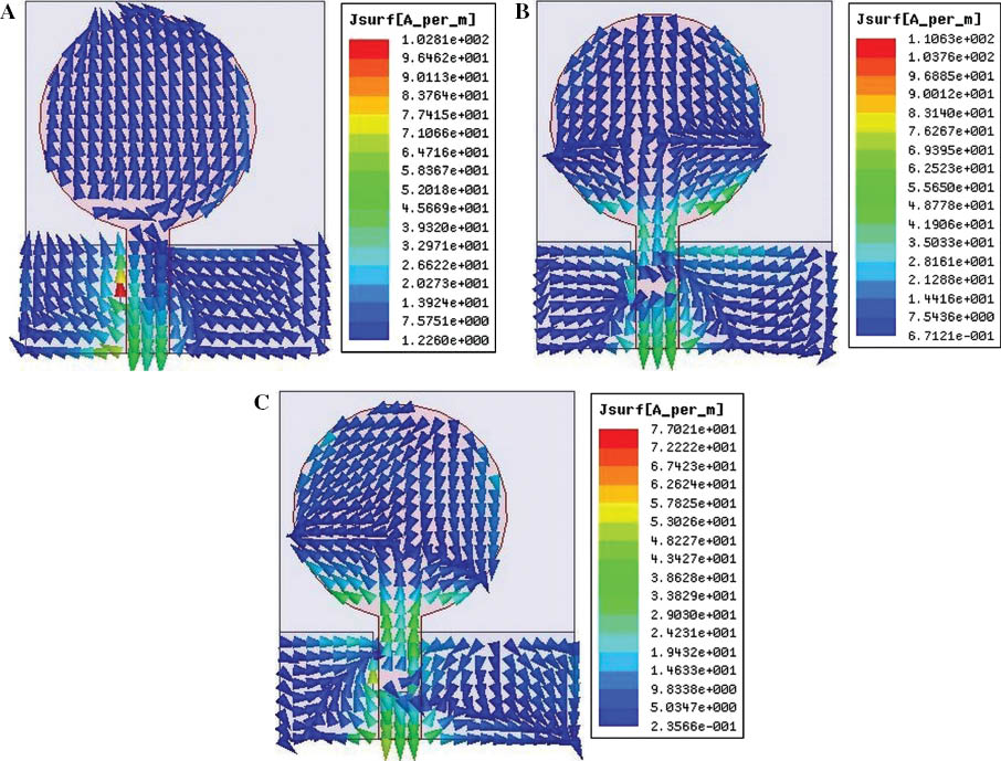
Surface current distribution at (A) 3.7 GHz, (B) 7.3 GHz, and (C) 9.2 GHz.
The current distribution can be shifted by changing the position or the lengths of the slots on both the partial ground plane and the radiator patch. It is regarded that the patch does not generate any significant variation in the current distribution for any shift in the position of the slots. In the current distribution, it is obvious from the analysis of variation, which is better excitation achievement at 3.7 GHz. At 3.7 GHz, current flow is equal to the lower and upper sections of the radiating patch. At 7.3 and 9.2 GHz, the current flow is prevalent at the inward and outward edges of the circular slot, and they are directed conversely. Consequently, the resultant radiations are obliterated and the antenna does not radiate effectively. The overall current flow is better on the upper portion of the radiating patch than on the lower portion, which is seen from the graph clearly at resonances of 7.3 and 9.2 GHz.
The measured UWB antenna radiation pattern is illustrated in Figure 14 for (A) E-plane at 3.7 GHz, (B) H-plane at 3.7 GHz, (C) E-plane at 7.3 GHz, (D) H-plane at 7.3 GHz, (E) E-plane at 9.2 GHz, and (F) H-plane at 9.2 GHz. To demonstrate copolarization and cross-polarization, 2D radiation patterns were reported at resonances of 3.7, 7.3, and 9.2 GHz, respectively. Eθ represents the copolarization properties and Eφ represents the cross-polarization properties. The yz coordinates are taken into account as the E-plane and xz coordinates are regarded as the H-plane. When the cross-polarization dimension is lower than the copolarization dimension, the antenna belongs to a standard radiation pattern. The cross-polarization dimension is smaller than the copolarization dimension on the H-plane at the resonances of 3.7, 7.3, and 9.2 GHz, respectively, and E-plane at 3.7 GHz. It is obvious that the mentioned UWB antenna with partial ground points out better broadside radiation features and considerable front-to-back ratio with low cross-polarization, which leads to symmetric and nearly omnidirectional radiation pattern.

Measured radiation pattern: (A) E-plane at 3.7 GHz, (B) H-plane at 3.7 GHz, (C) E-plane at 7.3 GHz, (D) H-plane at 7.3 GHz, (E) E-plane at 9.2 GHz, and (F) H-plane at 9.2 GHz.
5 Conclusion
A compact UWB antenna using epoxide woven glass fabric dielectric material has been proposed in this research, which nominates a single circular slot in the ground plane instead of a conventional ground with a view to obtaining UWB operation. This compact UWB antenna with a partial ground plane was designed and simulated using HFSS software (Ansoft, USA) as well as the current distribution plots to verify the proposed track. Finally, it was fabricated and measured to validate the performance of UWB. The measurements exhibited good understanding with the simulation results. Ultimately, the proposed UWB antenna along with a partial ground plane on epoxy woven glass material can be an appropriate for UWB applications.
Acknowledgments
This work is supported by the Ministry of Education Malaysia (MOE), Malaysia under grant no. FRGS/1/2014/TK03/UKM/01/1.
References
[1] Federal Communications Commission Revision of Part 15 of the Commission’s Rules Regarding Ultra-Wideband Transmission System from 3.1 to 10.6 GHz, in Federal Communications Commission: ET-Docket, 98–153, 2002.Search in Google Scholar
[2] Islam MM, Faruque MRI, Islam MT. Electron. World 2014, 120, 36–38.10.3329/jbas.v38i2.21346Search in Google Scholar
[3] Samsuzzaman M, Islam M. Microw. Opt. Technol. Lett. 2015, 57, 445–452.10.1002/mop.28872Search in Google Scholar
[4] Azenui NC, Yang HYD. IEEE Antennas Wirel. Propag. Lett. 2007, 6, 113–116.10.1109/LAWP.2007.891522Search in Google Scholar
[5] Ren YJ, Chang K. Electron. Lett. 2006, 42, 447–449.10.1049/el:20060210Search in Google Scholar
[6] Nazli H, Bicak E, Turetken B, Sezgin M. IEEE Antennas Wirel. Propag. Lett. 2010, 9, 264–267.10.1109/LAWP.2010.2046999Search in Google Scholar
[7] Islam MM, Faruque MRI, Islam MT. Sci. World J. 2014, 2014.10.1155/2014/791521Search in Google Scholar
[8] Ren YJ, Chang K. IEEE Antennas Wirel. Propag. Lett. 2006, 5, 274–276.10.1109/LAWP.2006.875897Search in Google Scholar
[9] Rajgopal SK, Sharma SK. IEEE Trans. Antennas Propag. 2009, 57, 1353–1359.10.1109/TAP.2009.2016694Search in Google Scholar
[10] Ma TG, Tseng CH. IEEE Trans. Antennas Propag. 2006, 54, 1105–1110.10.1109/TAP.2006.872562Search in Google Scholar
[11] Islam MM, Islam MT, Samsuzzaman M, Faruque MRI, Misran N, Mansor MF. Materials 2015, 8, 392–407.10.3390/ma8020392Search in Google Scholar PubMed PubMed Central
[12] Liang J, Chiau CC, Chen X, Parini CG. IEEE Trans. Antennas Propag. 2005, 53, 3500–3504.10.1109/TAP.2005.858598Search in Google Scholar
[13] Islam MM, Islam MT, Faruque MRI. Sci. World J. 2013, 2013.10.1155/2013/378420Search in Google Scholar PubMed PubMed Central
[14] Azim R, Islam MT, Misran N. Arab. J. Sci. Eng. 2013, 38, 2415–2422.10.1007/s13369-013-0553-xSearch in Google Scholar
[15] Matin MM, Sharif BS, Tsimenidis CC. IEEE Trans. Antennas Propag. 2007, 55, 2385–2388.10.1109/TAP.2007.901924Search in Google Scholar
[16] Faruque MRI, Islam MT, Mohamed NAN. Sci. Eng. Compos. Mater. 2014, 21, 79–85.10.1515/secm-2013-0044Search in Google Scholar
©2017 Walter de Gruyter GmbH, Berlin/Boston
This article is distributed under the terms of the Creative Commons Attribution Non-Commercial License, which permits unrestricted non-commercial use, distribution, and reproduction in any medium, provided the original work is properly cited.
Articles in the same Issue
- Frontmatter
- Original articles
- Micro-XCT-based finite element method for predicting the elastic modulus of needle carbon-fiber-reinforced ceramic matrix composites
- A comparative analysis of evolutionary algorithms in the design of laminated composite structures
- Study on the impact of Fe2P phase on the electrochemical performance of LiFePO4
- Improved hydration resistance of magnesia by EDTA and ammonium phosphate as additives
- The interaction of delignification and fiber characteristics on the mechanical properties of old corrugated container fiber/polypropylene composite
- The effects of thermal residual stresses and interfacial properties on the transverse behaviors of fiber composites with different microstructures
- Impact response characterization of shear CFRP strengthened RC beams by Fourier and wavelet methods: tests and analyses
- Nanoscale investigation of polymer cement concretes by small angle neutron scattering
- Design of a compact UWB antenna with a partial ground plane on epoxy woven glass material
- Preparation of polyimide-graphite composite and evaluation of its friction behavior at elevated temperatures
- Finite element analysis of mechanical properties of woven composites through a micromechanics model
- Tensile strength of Z-pinned laminates in RTD and hot-wet environment
- Free vibration analysis of symmetrically laminated composite circular plates with curvilinear fibers
- Preparation and characterization of nano NC/HMX composite particles
- Effect of heat treatment on the mechanical and tribological properties of AA8090/6% SiCp composite
- Design and absorption analysis of a new multiband split-S-shaped metamaterial
- Effect of matrix temperature and powder size on the infiltration height of SiO2-reinforced Al 7075 matrix composites produced by vacuum infiltration
- Optimization of preparation conditions of epoxy-containing nanocapsules