Artificial optoelectronic synapse based on CdSe nanobelt photosensitized MoS2 transistor with long retention time for neuromorphic application
-
Xiaohui Song
 ,
Xiaojing Lv
,
Xiaojing Lv


Abstract
Optoelectronic synaptic devices have been regarded as the key component in constructing neuromorphic computing systems. However, the optoelectronic synapses based on conventional 2D transistor are still suffering low photosensitivity and volatile retention behavior, which can affect the recognition accuracy and long-term memory. Here, a novel optoelectronic synaptic device based on surface-state-rich CdSe nanobelt photosensitized 2D MoS2 transistor is demonstrated. Benefiting from the excellent light absorption of CdSe and effective charge trapping at the hetero-interface, the device exhibits not only high photosensitivity but also long retention time (>1,500 s). In addition, typical synaptic functions including the excitatory postsynaptic current, paired-pulse facilitation, the transformation from short-term to long-term plasticity, the transformation from short-term to long-term plasticity, spike-amplitude-dependent plasticity, and learning-forgetting-relearning process are successfully simulated and modulated by light stimulation. Most importantly, an artificial neural network is simulated based on the optical potentiation and electrical habituation characteristics of the synaptic devices, with recognition accuracy rates of 89.2, 93.8, and 91.9 % for file type datasets, small digits, and large digits are achieved. This study demonstrates a simple and efficient way to fabricate highly photosensitive optoelectronic synapse for artificial neural networks by combining the merits of specific materials and device architecture.
1 Introduction
Inspired by human brain, artificial neuromorphic computing has emerged as a promising approach to overcome the von Neumann bottleneck. As the basic unit of neuromorphic computing system, synapses play significant role in transmitting information between two neurons, designing artificial synaptic devices is the key step to construct brain-like computers [1]. Compared to the traditional electric-stimulated synaptic devices, the light-stimulated synaptic devices (optoelectronic synapse) that driven by optical signals to realize synaptic functions offer the advantages of high bandwidth, low cross-talk, and low power consumption [1], [2]. More importantly, the optoelectronic synapses have great opportunity in artificial visual perception system as they could detect light signals, store and process data in the same device [2], [3], [4].
Up to now, various optoelectronic synaptic devices based on perovskites [5], [6], organic materials [7], [8], nanowires [2], amorphous oxide semiconductors [9], [10], and transition metal dichalcogenides (TMDCs) [11], [12], [13], [14] have been extensively investigated to emulate the function of biological synapses. Among them, TMDCs are especially worth exploiting because of their excellent electric field tunability, remarkable optoelectronic conversion efficiency, and easy integration with other dimensional materials [13], [14]. As reported, some devices based on 2D/2D vdWHs have been shown enhanced synaptic performance. Wang et al. demonstrated the artificial synapse transistor based on a fully 2D inorganic/organic (MoS2/PTCDA) hybrid heterostructure, and the carriers transfer at the heterojunction interface results in an excellent synaptic plasticity [15]. Yang et al. reported the Bi2O2Se/graphene hybrid structures for applications as photodetectors, neuromorphic devices, and digital logic operations. By using the positive and negative photoresponse characteristics induced by the excitation wavelength, major synaptic functions are achieved [16]. Due to the narrow bandgap and strong absorption of near-infrared (NIR) light of Bi2Se3, Wang et al. fabricated the MoSe2/Bi2Se3 heterojunction for mimicking hetero-synaptic plasticity, and NIR was used to control the device’s conductivity and synaptic plasticity [17]. Chen et al. combined 2D ferroelectric α-In2Se3 with p-type GaSe as the active layer to form a synapse device. Pavlovian conditioning was mimicked by combining light pulses with electrical pulses [18]. Although great progress has been achieved, the poor light absorption of atomic thick TMDCs that results in limited light–matter interactions [19], [20] and inferior photoresponse performance based on conventional 2D/2D vdWHs, thus requiring high-power light stimulus for programming operations. Furthermore, the long-term memory ability still faces many challenges with respect to neuromorphic applications [21], [22]. This is largely due to the rapid detrapping behavior of the trapped photocarriers at the 2D/2D heterojunction interface. To address the above challenges, the integration of surface-state-rich photosensitive materials with TMDCs has been identified as an effective approach to construct high-performance phototransistor synapse [23], [24], [25], [26]. As they could improve the light absorption, enhance photocarrier separation efficiency, and enlarge the application range. Furthermore, the defects on the surface of non-layered 2D materials generate localized electronic states, which could serve as charge-trapping centers to trap electrons or holes and thus improve the synaptic properties. Therefore, it needs to investigate the specific optical materials and optimized device structure to simulate synaptic plasticity behavior under optical stimulation.
In this work, we designed and fabricated an optoelectronic synaptic device based on CdSe nanobelt/MoS2 vertical vdWH transistor, where CdSe and MoS2 respectively act as the photosensitive and channel layer. The interaction between CdSe and MoS2 enhances the separation efficiency of the photoexcited carriers, thereby improving the photoresponsivity and synaptic plasticity of the device. In addition, the introduction of CdSe induces delayed decay of the photocurrent in MoS2, resulting a long retention time exceeding 1,500 s under 405 nm illumination, which serves as the basis for emulating essential synaptic behaviors, including excitatory postsynaptic current (EPSC), paired-pulse facilitation (PPF), short/long-term memory (STM/LTM), and learning-forgetting-relearning process under light stimulation. Most importantly, based on the optical potentiation and electrical habituation properties of the device, an artificial neural network (ANN) is stimulated based on the CdSe/MoS2 synapse with maximum image recognition accuracy up to 91.9 %.
2 Experimental section
2.1 Fabrication of MoS2 transistor
The MoS2 transistor was prepared by a dry transfer method [27]. A large-area multilayered MoS2 nanosheet was mechanically exfoliated on top of the PDMS film and transferred onto the SiO2 (300 nm)/Si substrate on a transfer platform equipped with an optical microscope (Shanghai OnWay Technology Co., Ltd). Next, the source and drain electrodes were patterned by a maskless ultraviolet lithography machine (TuoTuo Technology (Suzhou) Co., Ltd.). Then Au (ZhongNuo Advanced Material (Beijing) Technology Co., Ltd) metal contacts with a thickness of 40 nm were deposited by using thermal evaporation with a lift-off process in acetone.
2.2 Preparation of CdSe nanobelts
CdSe powder placed in the central area of the tube furnace was used as the source material. Some chips of SiO2 (300 nm)/Si coated with 10 nm-thick Au were used as the growth substrates and placed in the downstream area of the tube furnace. Prior to the growth process, the quartz tube was pumped to vacuum by a pump. Afterwards, the high-quality Ar was introduced into the quartz tube and the flow rate was maintained at 100 sccm. Then, the temperature of the tube furnace was increased to 850 °C and kept for 40 min. After the reaction, the black products would be synthesized on the substrates.
2.3 Fabrication of CdSe nanobelt photosensitized MoS2 transistor
The cured polyvinyl alcohol (PVA) was attached to PDMS to form a PDMS/PVA stamp. The prepared CdSe nanobelts were transferred to a new SiO2/Si substrate with a contact printing method. The selected CdSe flake was picked up with the PDMS/PVA stamp and then aligned and precisely laminated on top of MoS2 channel without contacting the metal electrodes. As a result, a CdSe/MoS2 vertical heterojunction was formed.
2.4 Material and device characterization
Raman spectroscopy was measured by using a Horiba Raman system with 532 nm laser excitation to analyze the heterojunction. Local contact potential difference (CPD) between CdSe and MoS2 constructed on ITO substrates was investigated with KPFM. A commercial AFM (Dimension Icon, Bruker) in peak force mode KPFM was used to carry out morphology and surface potential measurements. The topographic imaging was performed in tapping mode. After that, the surface potential images were acquired with the tip lifted to a height of about 20 nm. In the KPFM measurements, a bias was applied on the tip, with a scan rate of 0.5 Hz. Tips of KPFM measurements coated Pt/Ir layer with a typical tip radius of ∼20 nm. All the electrical properties and biological synaptic characteristics of the device were measured at room temperature using a probe station equipped with a microscope and a B1500A semiconductor parameter analyzer (Keysight). Optical signals were provided by laser source with 405 nm wavelength and the radius of the laser spot is about 0.2 cm.
3 Results and discussion
The CdSe nanobelt photosensitized MoS2 transistor was fabricated on a SiO2/Si substrate via PVA-assisted transfer method. Figure 1a and b show the schematic diagram and optical microscopic image of the CdSe/MoS2 heterojunction transistor, respectively. As shown in Figure S1, the physical vapor deposition (PVD) synthesized CdSe nanobelts have a width of a few micrometers, length of tens of micrometers. The XRD pattern is shown in Figure 1c, and all diffraction peaks can be indexed to the hexagonal structure of CdSe [28]. The thickness of MoS2 and CdSe measured by AFM is about 6 and 118 nm, respectively (Figure 1d). In order to characterize the optical properties of each layer and interface quality, Raman and UV–vis absorption were performed. The Raman spectrum of individual MoS2 and CdSe are shown in Figure 1e. Two obvious Raman peaks are observed at 378 cm−1 and 403 cm−1 for MoS2. In the Raman spectrum of CdSe, three distinct peaks presented at about 167 cm−1, 196 cm−1 and 406 cm−1, respectively. These Raman peaks are in consistent with previously reported data [29], [30]. For the CdSe/MoS2 heterojunction, all the above Raman peaks maintained and no noticeable peak position shift was observed, confirming the formation of high interface quality after the device fabrication. In Figure 1f, MoS2 has a low absorption in the visible range, and CdSe nanobelt exhibits strong light absorption in the range of 380–750 nm, covering almost the whole visible light region, while the absorption intensity of CdSe/MoS2 heterojunction is greatly enhanced compared to individual MoS2 and CdSe. This suggests that CdSe can act as an absorption layer of visible light to enhance the photoresponsivity and synaptic plasticity.
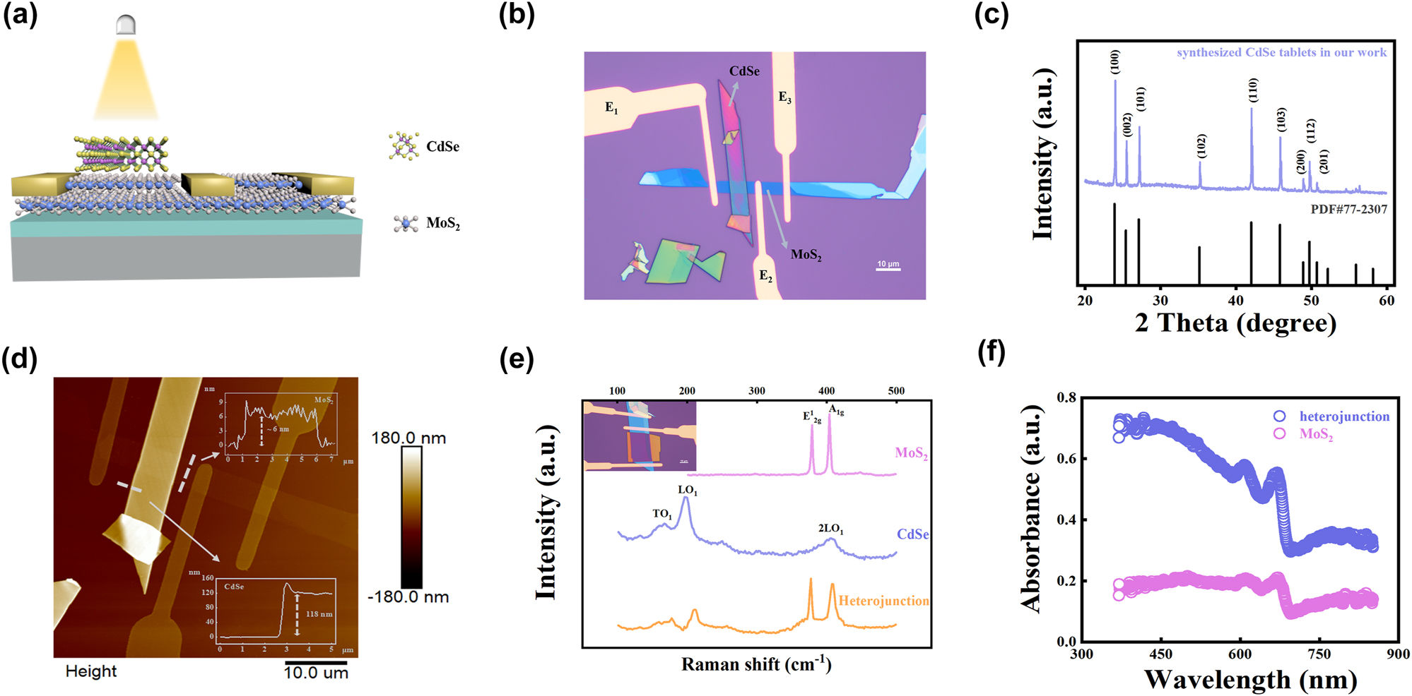
Design and characterization of CdSe/MoS2 device. (a) Schematic diagram of the CdSe/MoS2 vdWH device. (b) Optical microscopic image of the device. (c) XRD pattern of CdSe synthesized by PVD and comparison with standard card. (d) AFM image of CdSe/MoS2 device. (e) Raman spectrum of CdSe and MoS2 under 532 nm laser excitation. (f) UV–vis absorption spectra of MoS2 nanosheets, CdSe nanobelt, and CdSe/MoS2 heterojunction.
Figure 2a schematically depicts the diagram of the human visual nervous system. As external visual information coming from an object was focused onto the retina, the information is transmitted through the optic nerve and processed in the visual cortex [31]. The brain constantly receives, analyzes, stores information and makes decisions to achieve a variety of complex functions, depending on the synapse that exists between neurons. As shown in the right picture of Figure 2a, in biological neural network, the synapse is the connection between a pre-synaptic and a post-synaptic neuron. An external stimulus induces an action potential at pre-synaptic terminal, making the neurotransmitters released by pre-synaptic membrane and dock with the receptors on the post-synaptic neuron, resulting in the generation of excitatory post-synaptic current (EPSC) or inhibitory post-synaptic current (IPSC) in postsynaptic neuron. When the external stimulus is removed, the neurotransmitters in the post-synaptic membrane will gradually disappear, and thus the post-synaptic current slowly returns to its original state. This behavior is responsible for learning and memory behavior for synapse [7]. Inspired by the brain and visual nervous system, the CdSe/MoS2 phototransistor can be used to simulate the function of biological synapses. By analogy with biological synapses, the gate voltage or the laser stimulation can be regarded as a presynaptic input, while the source/drain electrodes serve as the postsynaptic output terminal, and channel conductance is defined as the synaptic weight.

The electrical characterization of the CdSe/MoS2 device. (a) The left schematic is the human visual system. The right shows the comparison between biological synapse and the CdSe/MoS2 optoelectronic synapse. (b) Transfer curve of the CdSe/MoS2 device in dark at V d = 1 V. The inset is the double-sweeping transfer curves with different sweeping ranges. (c) The KPFM image of the heterostructure. The inset is the optical image of the device based on ITO substrate. (d) The surface potential profile along the white line in the KPFM image. (e) The band alignment of the CdSe/MoS2 heterostructure. (f) The time-resolved retention performance of the CdSe/MoS2 after applying a positive and negative V g pulse with 10 ms duration. (g) The EPSC excited by negative V g pulses with different amplitudes, which shows the transition from STM to LTM behavior. (h) Long-term potentiation/depression characteristics for the CdSe/MoS2 transistor.
Figure 2b shows the ambient double-sweep transfer curve of a typical CdSe/MoS2 transistor at V ds = 1 V under dark condition. The device exhibits a typical n-type transport behavior with a high on/off ratio (≈107). Moreover, as shown in the inset, the hysteresis window increases with the incremental of gate voltage sweeping, and a maximum window of 75 V was observed under −80 to 80 V sweeping. In comparison, the bare MoS2 transistor without CdSe layer showed a much smaller hysteresis window (Figure S2a), indicating a lower trapped charge density compared to the CdSe/MoS2 heterojunction. Previous studies have demonstrated the hysteresis can be attributed to the interfacial traps at the MoS2/SiO2 and the intrinsic defects in MoS2 [32], [33], [34]. Due to the same batch of SiO2/Si substrates and similar thickness of MoS2 were used, the larger hysteresis window of CdSe/MoS2 device can be attributed to interaction between CdSe and MoS2.
To investigate the band alignment between CdSe and MoS2, the Kelvin probe force microscopy (KPFM) mapping image of this vdWH is measured in dark and the result is shown in Figure 2c. The contact potential difference (CPD) between the sample and the KPFM tip is calculated by the following equation [35]:
where W tip , W MoS2 , and W CdSe are the work function of the tip (Pt/Ir-coated Si), MoS2, and CdSe, respectively. The variation in CPD between MoS2 and CdSe is given by
Figure 2d presents the variation of the surface potential along the dashed line across the heterojunction region in Figure 2c. It can be seen clearly observed that the surface potential of MoS2 is ∼250 mV larger than that of CdSe. Therefore, the Fermi level of MoS2 is 250 meV higher than that of CdSe.
Based on the KPFM results and previously reported band properties of CdSe and MoS2 [36], [37], the energy band alignment is graphically described in Figure 2e. A type-II band alignment is formed between CdSe and MoS2, which is consistent with that calculated theoretically based on density functional theory (DFT). The calculation details and results are shown in Figures S3 and 4. Since the E f of MoS2 is higher than that of CdSe, some electrons in MoS2 will diffuse to CdSe after contact and be trapped by the defects in CdSe. These electrons, together with that trapped at MoS2/SiO2 interface, serve as the local gate and result in a larger hysteresis window relative to pristine MoS2.
Figure 2f shows the retention properties of the CdSe/MoS2 device that record after an individual V g pulse at V ds = 1 V. When a positive voltage pulse (100 V, 10 ms) was applied to the gate electrode, the electric field induced a specific number of electrons in MoS2 were captured by the traps at the MoS2/SiO2 and the intrinsic defects in MoS2 (Figure S5a). At the end of the pulse, the channel current, namely, post-synaptic current (PSC), was driven to a low level of 0.06 pA due to the electrons trapped in MoS2 and at SiO2/MoS2 interface acted as local gate (Figure S5b). As exhibited in Figure 2f, the inhibitory post-synaptic current (IPSC) is followed by an increase process of ∼200 s before stabilizing at 118 pA, which may be due to some trapped electrons relaxed back to MoS2, so that the carrier density in the channel increases. On the other hand, when a negative pulse (−80 V, 10 ms) was applied to gate, the negative voltage pushed the electrons trapped at the MoS2/SiO2 interface and the defects of MoS2 into the MoS2 channel (Figure S5c). After the V g was removed, the strength of local gate was reduced and MoS2 was switched to the high-conductance state (Figure S5d), and thus a high excitatory postsynaptic current (EPSC) of 2.12 µA was obtained, resulting in a stable on/off current ratio over 103 was achieved for 1,500 s. The charge trapping and de-trapping process in CdSe/MoS2 device offers the basic condition for mimicking the synaptic functionality. The similar retention change has also been observed in bare MoS2 devices in Figure S2b. Due to the lack of the CdSe layer for trapping electrons, the local gate after positive V g pulse is smaller than that in CdSe/MoS2 device, thus the IPSC is two orders of magnitude larger than that for CdSe/MoS2 device, and the on/off current ratio was reduced to 10 for pristine MoS2 transistor (Figure S2b).
In biological systems, short-term memory (STM) only lasts for seconds or tens of minutes, while long-term memory (LTM) can last from a few hours and even to a lifetime [26]. Figure S6 shows a schematic diagram of the memory consolidation process in the human brain. The STM can transform into LTM through increasing learning times or intensity. In this CdSe/MoS2 device, the transition from STM to LTM was successfully imitated by changing the amplitude of gate voltage. Figure 2g shows the time-dependent postsynaptic current (PSC) induced by a negative voltage pulse with same width of 10 ms but different amplitudes. The PSC increases immediately after a −40 V gate pulse and decays to the initial value after 300 s. This behavior is similar to the STM in our brain. As the amplitude of the gate pulse is increased, an LTM was achieved, which is characterized by the increased PSC and decay time than that of the −40 V ones. This is because stronger input pulse could drive more trapped electrons into the channel, leading to a higher EPSC, and the decay of EPSC would continue before some free electrons got trapped again and achieved a balance.
Long-term synaptic plasticity is composed of long-term potentiation (LTP) and long-term depression (LTD) of synaptic weights, which is a significant constituent part of the control memory in hippocampal neurons [4]. LTP/LTD can be mimicked by applying high frequency spikes to enhance/reduce the synaptic transmission. To verify the LTP and LTD, 10/20/30/50 consecutive negative gate pulses (−50 V, 10 ms duration) and then 10/20/30/50 consecutive positive pulses (50 V, 10 ms duration) were applied to the gate electrode as presynaptic input, whereas drain current was continuously recorded as PSC. As shown in Figure S7a, the PSC could be modulated with a total of 10, 20, 30, and 50 cycles of V g pulses. The PSC increases more rapidly in the first 20 negative V g pulses and then slightly saturates as the pulse number increases to 30 and 50 (Figure 2h). In contrast, the PSC rapidly decreases and then saturates as the number of the positive V g pulses increase, suggesting the capability of CdSe/MoS2 device to mimic the LTP and LTD behavior of a synapse. Figure S7b represents the PSC response to six successively decreasing negative V g pulses (from −10 to −100 V) with a pulse duration of 10 ms, the PSC increases gradually due to more trapped electrons are driven to MoS2 layer, which can be used to mimic the potentiation of the synaptic strength. Afterward, under six successively increasing positive V g pulses (from 10 to 100 V, duration: 10 ms), more electrons are trapped at the interfacial SiO2 layer and defects of MoS2, thus the conductance of the device decrease gradually, corresponding to the habituation of the synaptic strength. The EPSC and IPSC can also be adjusted by the pulse amplitude. The PSC under a sequence of ten consecutive gate pulses with amplitude varying from −10 to −100 V was recorded in Figure S8a. The change of PSC after each pulse is extracted and plotted in the inset. It can be observed that the current increased by four orders of magnitude from 2.89 × 10⁻¹⁰ A at −10 V to 2.27 × 10⁻⁶ A at −100 V for a same pulse width of 10 ms. Similarly, the synaptic inhibitory behavior was observed by applying consecutive positive V g pulse, as shown in Figure S8b. The PSC continuously decreases as the pulse amplitude increases from 10 V to 100 V. Therefore, the CdSe/MoS2 device could respond to stimulation with different-amplitude to mimic the synaptic behavior of spike-amplitude-dependent plasticity (SADP).
In addition to modulating excitatory and inhibitory synaptic behaviors with electrical pulses, the device can also effectively imitate the neuromorphic function with light stimulation, owing to the strong light absorption of CdSe. To investigate the photoresponse characteristics of the CdSe/MoS2 device, the transfer curves of the device under different light intensities (λ = 405 nm) are measured and shown in Figure 3a. Under light illumination, the I ds exhibits an abrupt increment and left shift of the threshold relative to that in dark, which is caused by the increased charge carriers in MoS2 channel that mainly derived from the separation of photoexcited carriers at the CdSe/MoS2 hetero-interface. The photoresponsivity (R) of the device is plotted as the function of the power density according to the following equation [38]:
where I photo, I dark, P in, A are photocurrent, dark current, light power intensity, and effective area of the device. As shown in Figure 3c, the R varies with the gate voltage, and a maximum value reaches 3.624 × 10³ A/W at 2.22 mW/cm2 and V g = 10 V. This result indicates the CdSe/MoS2 heterojunction transistor is highly sensitive to visible light and has the potential to realize light stimulated synapse. Subsequently, the optically-programmable and electrically-erasable properties are investigated. Figure 3d shows the transfer curves of CdSe/MoS2 heterojunction before and after light illumination at V ds = 1 V. An optical pulse (405 nm, 10.84 mW/cm2, width of 10 s) was used for programming operation, while electrical pulse with a height of −100 V and a width of 10 ms was employed as erasing operation. After the optical programming operation, the transfer curve shifts toward the left direction, while the threshold voltage (V th) can be restored to its initial state after the electrical erasing operation.
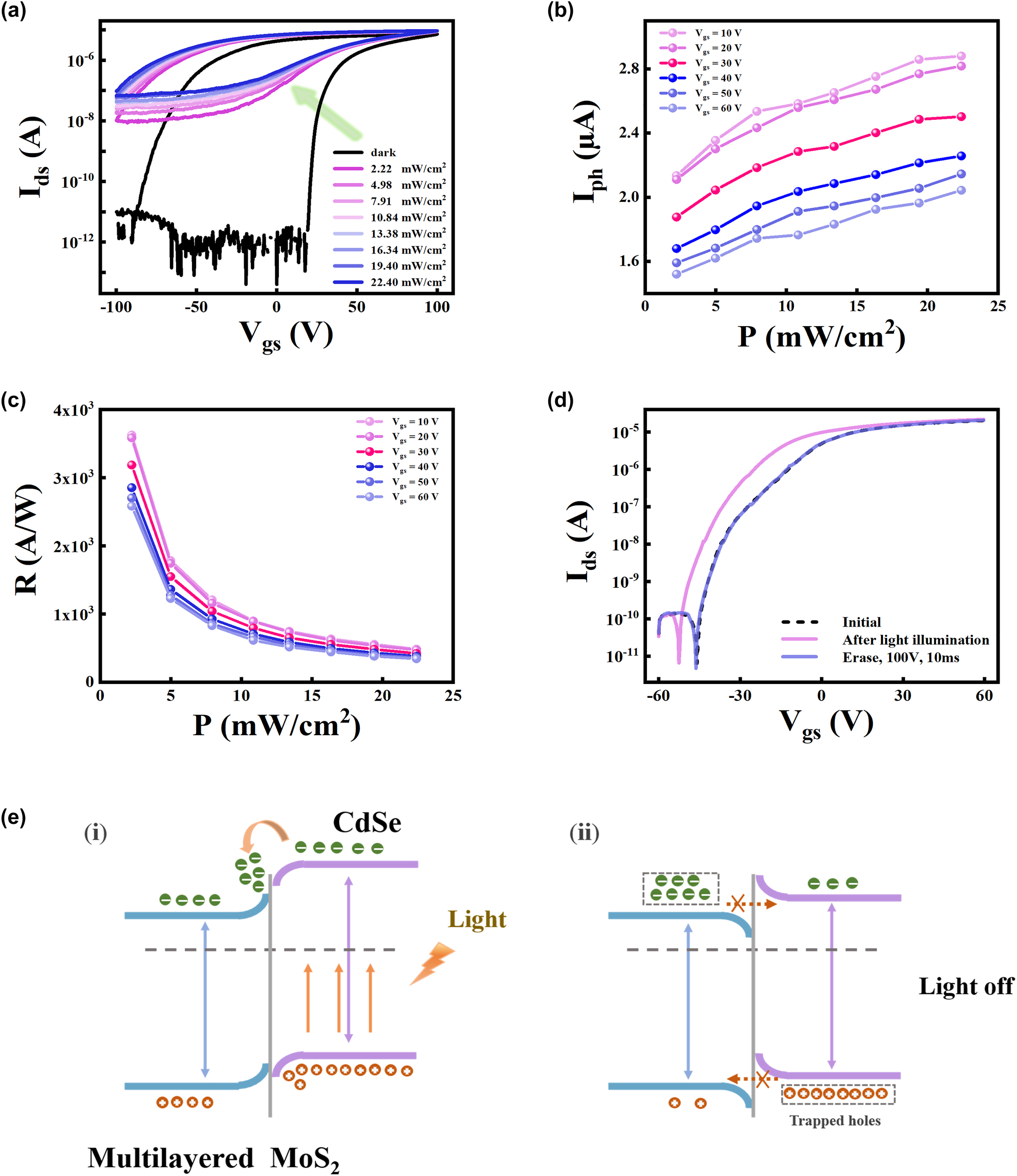
The energy-band diagrams of CdSe/MoS2 heterojunction and the transport of photogenerated carriers at the hetero-interface. (a) The double-sweep transfer curves of the device under dark condition and 405 nm laser with different power densities. (b) Photocurrent and (c) responsivity of the device under various light power intensities at different gate voltage. (d) The transfer curves of the CdSe/MoS2 device at initial state, optically programmed (450 nm, 10.84 mW/cm2 for 10 s) state and electrically erased (100 V for 10 ms) state. (e) Schematic diagram for charge generation and transport process at the CdSe/MoS2 interface under laser irradiation and after removing irradiation.
This phenomenon can be explained with band structure of the heterojunction. Due to the diffusion of electrons from MoS2 to CdSe after contact, a built-in electric field is formed directed from MoS2 to CdSe. As shown in Figure 3e, when light is illuminated on the device, a large number of electron-hole pairs are mainly photoexcited in the CdSe, and the electrons are quickly driven to the MoS2 by the built-in electric field, whereas the holes are confined in CdSe due to the energy barrier, resulting in a strong photogating effect even after removing the illumination, which leads to the negative shift of transfer curve. When electrical erasing operation (100 V, 10 ms) is applied, the electric field induces a specific number of electrons trapped at the MoS2/SiO2 interface, and thus the electron concentration in MoS2 channel is reduced and the Ids is restored to its initial state again.
To investigate the learning and memory behavior of the CdSe/MoS2 synaptic device, Figure 4 shows the time-dependent photoresponse of the device at V ds = 1 V after individual light pulse stimulation. As shown in Figure 4a, upon laser illumination (405 nm, 10.84 mW/cm2, duration = 1 s), the I ds rapidly increases up to 115.1 nA, corresponding to the EPSC behavior of biological synapse. When light illumination is removed, the I ds slowly decays to 90.73 nA during the first 2 s and then stabilizes at this value. The current level is much higher than the initial-state current of 1.14 × 10⁻¹² A, indicating a memory effect towards the light stimulus. This charge storage behavior is analogous to the long-term plasticity of biological synapses, which is prerequisite to ensure reliable study on the synaptic functions. A long retention time is required for achieving long-term memory. The memory retention time of the CdSe/MoS2 device was measured with the device trained by ten light pulses, where the EPSC decayed from 172 to 40 nA within 1,500 s after removing the light pulses. While the current for pristine MoS2 transistor is reduced from 22 to 2.6 nA within 32 s (Figure S9). The longer retention time for the CdSe/MoS2 device can be ascribed to the introduction of CdSe layer. When a laser pulse is applied, a large number of electron-hole pairs were generated in CdSe due to its excellent optical absorption properties, and then the electrons were transferred to MoS2 due to the built-in potential, resulting in a surge of PSC and negative shift of V th. While the holes are confined to CdSe due to the energy barrier, leading to a strong photogating effect, which increases the electron concentration in MoS2 channel. After removing the light stimulus, the slow recombination of electrons and holes induces the channel exhibiting a long-term conductive, which accounts for the slow conductance decay behavior for the CdSe/MoS2 synaptic device. This is a prerequisite for reliable study of synaptic photoresponse.
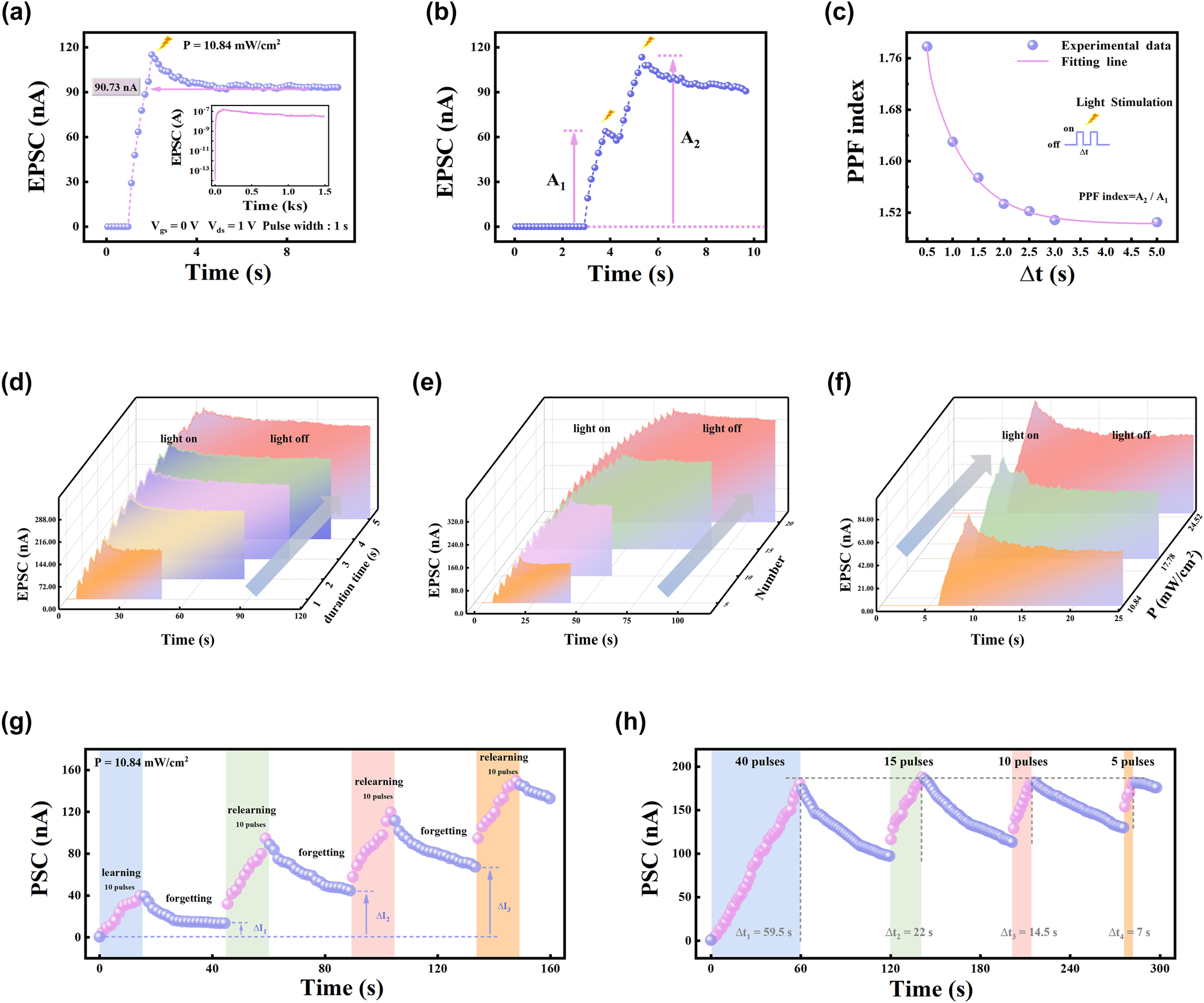
Optical synaptic behavior of the fabricated device. (a) The transient EPSC response triggered by a light spike (λ = 405 nm, 1 s, 10.84 mW/cm2). The inset is the long-memory retention performance of the transistors after removal of light source. (b) EPSC of the device excited by two adjacent laser pulses with an interval of 0.5 s. (c) The PPF index is plotted as a function of pulse interval time. The transition from short-term memory to long-term memory under successive light pulses by changing the (d) width, (e) number, and (f) intensity of light pulse using 405 nm laser (the reading voltage is fixed at 1 V). (g) The “learning-forgetting” process of four cycles. (h) The demonstration of the “learning-forgetting-relearning” process with the learning and relearning process reach up to the same level.
PPF is a typical short-term synaptic plasticity triggered by two consecutive presynaptic spikes, which is essential to decode temporal vision or auditory information in biology neural systems. It means that when two consecutive stimuli with a short time interval are applied, the amplitude of current changes caused by the second stimulus is larger than that caused by the first one [10]. The PPF behavior can be mimicked by applying two consecutive light stimulation with an interval time (Δt) to the CdSe/MoS2 device. As shown in Figure 4b, the amplitude of PSC triggered by the second laser pulse is significantly higher than that stimulated by the first, which is very similar to the PPF behavior in the biological synapses. The PPF index can be described as [19]:
where A 1 and A 2 represent the amplitudes of the PSC triggered by the first and second light pulses. The dependence of the PPF index on Δt is shown in Figure 4c. With the increases of Δt, the PPF index gradually decreases, and reaches a maximum value (178 %) at 0.5 s, suggesting the memory formation process can be accelerated by reducing the interval between stimulus. It is noteworthy that the PPF value is comparable to that of most previously reported optoelectronic synapse devices [19], [39] (Table 1). This is because the trapped photogenerated holes inside the CdSe layer need to take a long time to decay. Pink curve shows the fitting result of the decay trend by a double exponential function [39]:
where τ 1 and τ 2 represent the characteristic relaxation times of the rapid and slow phases. The fitting results show that τ 1 and τ 2 are 37 and 773 ms, respectively, and both values are close to that measured in the biological synapses (τ 1 = 40 ms, τ 2 = 300 ms) [40]. This feature indicates that learning and memory are associated with frequent and repetitive training.
Here, the transition from STP to LTP are further emulated in the CdSe/MoS2 device by altering light spike duration, number, and intensity, and these parameters can be deemed as the learning time, number, and intensity. Figure 4d shows the time-dependent EPSC characteristics of CdSe/MoS2 device under five laser spikes with different width. Clearly, as the spike width increases from 1 to 5 s, the cumulative spikes induced EPSC is increased by 4 times, and the decay time is prolonged and the stable current is increased, which indicates the transition of the synaptic plasticity from STM to LTM under the cumulative stimulation. Besides the spike width, as presented in Figure 4e and f, the number and intensity of light spikes can also be used to modulate the transition from STM to LTM. With the light pulse number (1–5) and pulse intensity (10.84–24.52 mW/cm2), the EPSC value gradually increased after the removal of light illumination, and the decay time of EPSC was prolonged. This phenomenon can be ascribed to the fact that longer illumination time (or stronger optical signals) result in higher carrier concentration in the MoS2 channel and more negative shift of V th due to the enhanced photogating effect. This phenomenon is consistent with the Atkinson–Shiffrin’s memory model that the short-term memories can be transferred into long-term memory through repeated learning [41]. In addition, the light wavelength-dependent EPSC of the device are investigated and the results are shown in Figure S10. It can be observed that light illumination with short wavelengths generates the larger PSC of 145.97 nA for 532 nm and 160.98 nA for 670 nm at the end of the spikes, while near-infrared light irradiation (808 nm) produces a low current of 5.74 nA, which is consistent with the UV–vis absorption spectrum of CdSe. Such optoelectronic synaptic device architecture should be applicable to other vdWHs. Figure S11 shows the schematic diagram of the fabricated light-stimulated CdSe/ReS2 synaptic device. Under dark condition, the device also exhibits a large hysteresis memory window. When light pulses are applied to the device, some typical synaptic behaviors, such as EPSC, PPF, and STM-LTM, are also successfully emulated in this device. The detailed information can be found in Figure S11.
Based on the above synaptic behavior of the CdSe/MoS2 device, the “learning-forgetting-relearning-forgetting” experience of human brain is emulated in this device. Figure 4g presents four cycles of “learning-forgetting” processes. The first learning process was performed by applying 10 light pulses (405 nm, 10.84 mW/cm2, duration of 1 s) at Vds = 1 V, which results in the channel current significantly increasing from 2.27 pA to 39.39 nA. After removing the light illumination, the PSC gradually decays to 13.04 nA within 30 s. This process corresponds to the forgetting process. The CdSe/MoS2 device can retain 33 % of the memory in the end, which indicates that some part of the information learned by the human brain will be forgotten after a period of time. However, memory loss with time can be improved by repeated learning. The post-synaptic conductance at the end of the forgetting process, corresponding to the cognitive level, increased gradually with the number of learning-forgetting cycles as indicated by ΔI 3 > ΔI 2> ΔI 1.
When 40 consecutive light pulses (λ = 405 nm, 1 s) are applied to the CdSe/MoS2 device during the first learning process, the PSC gradually increases from 0.16 to 180 nA (Figure 4h), indicating an increase in synaptic weights. Subsequently, the current decays to 96.8 nA after 60 s of forgetting process. In the second learning process, only 15 light pulses are needed to recover to the current level that the first learning process achieved, and this value further reduced to 10 and 5 in the third and fourth learning process, indicating that the relearning process becomes much easier. It can also be observed that the decay trend of the PSC slows down after relearning process. This trend is consistent with human’s “learning–forgetting–relearning–forgetting” model. It requires less time to relearn previously forgotten information than to learn for the first time, and timely review could reduce the forgetting rate and strengthen the memory capability. This result demonstrates the feasibility of the CdSe/MoS2 device in constructing the biological nervous system.
Except for natural forgetting, applying a positive gate voltage spike (100 V, 1 s) could directly erase the PSC to the initial state of CdSe/MoS2 device, as precisely shown in Figure 5a. This is because the positive gate voltage can induce many electrons in MoS2 channel trapped at the MoS2/SiO2 interface, which may depress the device to the initial low conductance state. Despite the stable long-term potentiation/depression (LTP/LTD) have achieved with electrical programming/erasing (Figure 2h), the asymmetry between LTP and LTD may reduce accuracy of pattern recognition, which is not expected in neuromorphic computing [42]. To overcome the shortcoming, the optical stimulation induced LTP and electrical spikes driven LTD synaptic behavior were successfully emulated with CdSe/MoS2 transistor. As shown in Figure 5b, the current increases gradually with 10/20 consecutive optical pulses (405 nm, 10.84 mW/cm2, duration of 1 s), which represent the potentiation of the synaptic weight. Subsequently, the current decrease gradually with same number of electrical pulses (V g amplitude uniformly increasing from 10 to 100 V, step = 10 V, pulse width of 10 ms), corresponding to the depression characteristics. The near-linear and symmetric potentiation-depression response is the basis of realizing high image recognition accuracy. To evaluate the endurance performance of potentiation-depression for the CdSe/MoS2 device, 40 cycles of photonic potentiation (1 s duration with 1 s interval) and electrical depression were tested, and the results shown in Figures 5c and S12a exhibit nearly less conductance variation between the first and last cycle, reflecting repeatable switching and good endurance of the device. During the entire 40 cycles measurement, the device is periodically switched between program and erase state, and the program/erase ratio is maintained above 104 (Figure S12b).
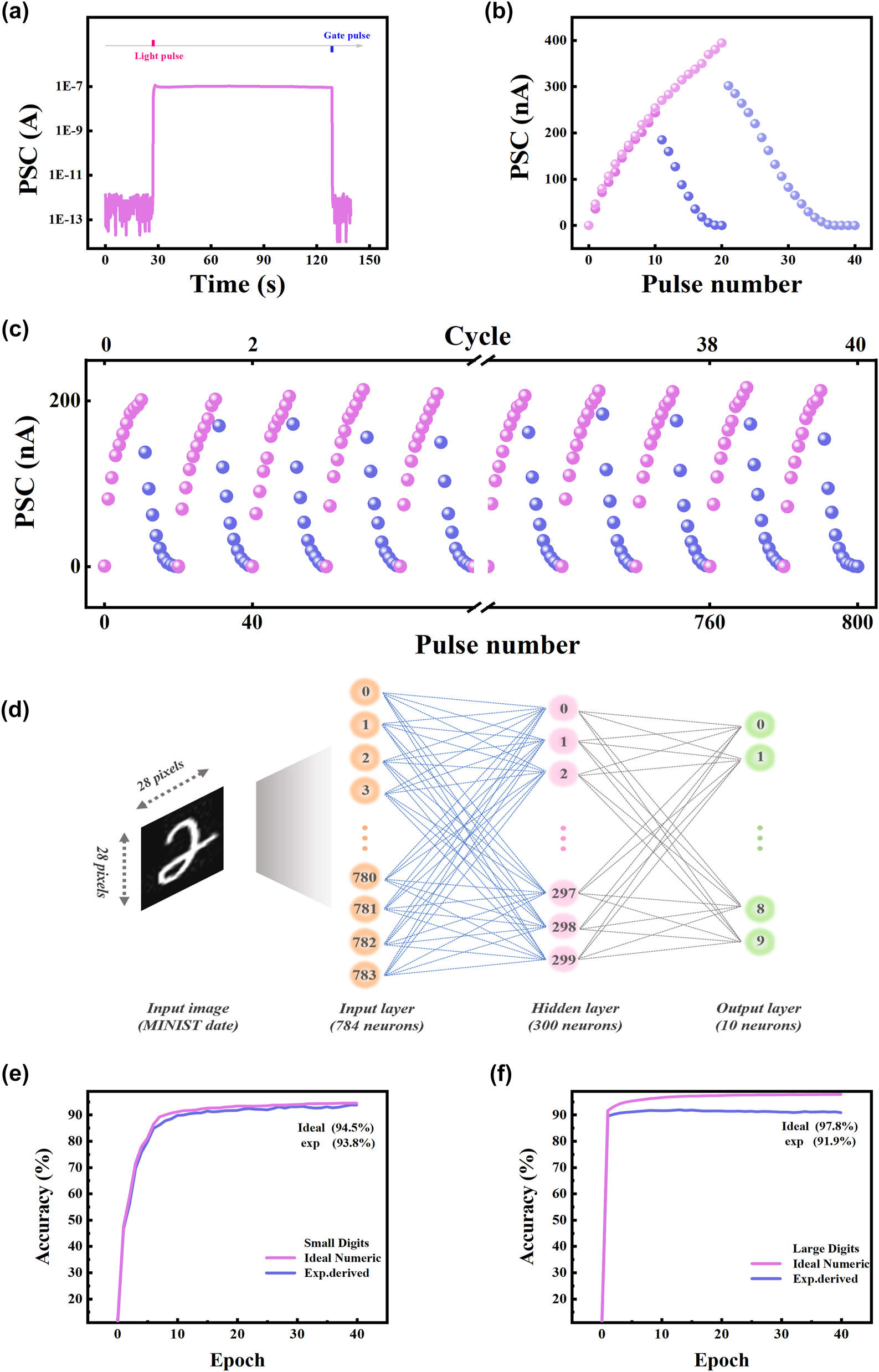
Simulation of artificial neural network for image recognition based on the CdSe/MoS2 synaptic device. (a) The programming and erasing operations of PSC by light pulse and gate voltage pulse. (b) Long-term potentiation/depression characteristics for the CdSe/MoS2 transistor triggered by 10/20 successive light pulses and then 10/20 gate voltage pulses. (c) The 40 cycles of long-term potentiation/depression curve based on CdSe/MoS2 synaptic transistor. (d) Schematic illustration of neural network for recognition of large image tasks. The simulated recognition rate as a function of training epochs for the (e) small image and (f) large handwritten digits.
The cycle-to-cycle reproducibility demonstrates high stability and switching endurance of the CdSe/MoS2 device. To evaluate the learning ability of CdSe/MoS2 synaptic devices, an artificial neural network (ANN) with a three-layer structure was constructed for handwritten digit recognition. As shown in Figure 5d, the network is consisting of the input layer (784 neurons), hidden layer (300 neurons), and output layer (10 neurons), where the input layer corresponds to 28 × 28 pixels input image from the “Modified National Institute of Standards and Technology” (MNIST) dataset, and the output layer corresponds to 10 categories that recognize the numbers 0 to 9. The ANN was trained with the back-propagation algorithm using three datasets: small images with 8 × 8 pixels of handwritten digits, large images with 28 × 28 pixels of handwritten digits from the MNIST dataset, and a Sandia file classification dataset. The conductance states of the CdSe/MoS2 synaptic transistor are used as a weight update for performing back-propagation based on the experimental results of the 40 cycles of optical potentiation and electrical depression curve. The pattern recognition accuracy of CdSe/MoS2 device and ideal synapse for file types, small and large digits are presented in Figures 5e, f and S12c, respectively. The simulation results of the artificial neural network under ideal conditions indicate the limit of algorithm accuracy, which is plotted by the pink curve. After 40 training epochs, the file types recognition accuracy based on CdSe/MoS2 device is 89.2 %, which is close to the ideal value (93.3 %). The recognition accuracy of small images reaches up to 93.8 %, which is almost the same as the ideal value (94.5 %). For the simulations of large images with 28 × 28 pixels also obtain a high accuracy of 91.9 %, which is comparable or higher than that of most reported optoelectronic synaptic devices [43], [44], [45] (Table 1). Such remarkable recognition accuracy can be attributed to the linear tendency of channel conductance. These excellent performances demonstrate the possibility of the CdSe/MoS2synaptic device for the construction of artificial neural networks in applications of neuromorphic computing.
Comparison of recognition accuracy and PPF index among different artificial synaptic devices.
| Materials | Wavelength (nm) | Pulse (s) | PPF (%) | Accuracy (%) | Epoch | Ref. |
|---|---|---|---|---|---|---|
| MoS2/PTCDA | 532 | 0.4 | 147 | NA | NA | [39] |
| Bi2O2Se/graphene | 635 | 0.1 | 120 | NA | NA | [16] |
| Cs2AgBiBr6/IGZO | 365 | 30 | 206.9 | 83.8 | 18,000 | [43] |
| Cs3Bi2I9/PMMA/DPPDTT | 405 | 1 | 122 | 92.1 | 10,000 | [46] |
| ZnO/PbS | 365 | 0.2 | 46 | 67 | 4,000 | [47] |
| BP flakes | 280 | 10 | NA | 90 | 1,000 | [44] |
| IGZO-alkylated/graphene | 405 | 0.05 | 182 | 62 | 36,000 | [48] |
| UCNPs-MoS2 | 980 | 5 | 190 | 70 | 15,000 | [49] |
| WSe2/h-BN flakes | 655 | 0.01 | NA | 90 | 50 | [45] |
| CuPc/p-6P thin films | 365 | 0.5 | NA | 78 | 5,000 | [50] |
| CdSe/MoS2 | 405 | 1 | 178 | 91.9 | 40 | This work |
4 Conclusions
In summary, a highly photosensitive optoelectronic synaptic device is demonstrated based on CdSe nanobelt sensitized 2D MoS2 transistor. The device combines efficient light absorption layer, high mobility channel material, and efficient charge transfer, leading to excellent electric tunability and superior photoresponse characteristics. The photogating effect at the CdSe/MoS2 interface results in a long retention time exceeding 1,500 s, which provides the basis for achieving efficient light-stimulated synaptic behaviors, such as EPSC, STM-LTM, PPF, SADP, and learning–forgetting–relearning process. The synaptic potentiation and depression can be modulated under the stimulation of optical and specific electrical pulses, respectively. In addition, the recognition accuracy of handwritten digits with 28 × 28 pixels in MNIST dataset reaches up to 91.9 % after 40 training epochs by using a three-layer ANN, which is higher than most of reported optoelectronic synaptic devices. This work provides a simple and attractive strategy for the fabrication of optoelectronic synaptic devices for neuromorphic computational networks.
Supporting Information
The characterization of the pristine MoS2 nanobelt and FETs, the details of the DFT calculation and the calculated band structure of CdSe/MoS2 heterojunction, schematic of interface traps that capture and release electrons, schematic diagram of the memory consolidation process in the human brain, performance of potentiation-depression with consecutive 4 sets of different electrical pulse numbers, the retention performance of bare MoS2 transistors, and the characteristics of the artificial optoelectronic synaptic device based on the CdSe/ReS2 heterojunction.
Funding source: The Key Scientific Research Projects of Colleges and Universities in Henan Province
Award Identifier / Grant number: 24A140012
Funding source: Natural Science Foundation of Henan Province
Award Identifier / Grant number: 242300421407
Funding source: National Natural Science Foundation of China
Award Identifier / Grant number: 62374054
-
Research funding: Natural Science Foundation of Henan province in China (General Program, Grant No. 242300421407), National Natural Science Foundation of China (General Program, Grant No. 62374054), the Key Scientific Research Projects of Colleges and Universities in Henan Province (No. 24A140012).
-
Author contributions: All authors have accepted responsibility for the entire content of this manuscript and approved its submission.
-
Conflict of interest: Authors state no conflicts of interest.
-
Informed consent: Informed consent was obtained from all individuals included in this study.
-
Ethical approval: The conducted research is not related to either human or animals use.
-
Data availability: Data underlying the results presented in this paper are not publicly available at this time but may be obtained from the authors upon reasonable request.
References
[1] Y. Li and G. Z. Shen, “Advances in optoelectronic artificial synapses,” Cell Rep. Phys. Sci., vol. 3, no. 9, p. 101037, 2022. https://doi.org/10.1016/j.xcrp.2022.101037.Suche in Google Scholar
[2] X. Chen, et al.., “Nanowires for UV–vis–IR optoelectronic synaptic devices,” Adv. Funct. Mater., vol. 33, no. 1, p. 2208807, 2023. https://doi.org/10.1002/adfm.202208807.Suche in Google Scholar
[3] J. Lee, et al.., “Light-enhanced molecular polarity enabling multispectral color-cognitive memristor for neuromorphic visual system,” Nat. Commun., vol. 14, no. 1, p. 5775, 2023. https://doi.org/10.1038/s41467-023-41419-y.Suche in Google Scholar PubMed PubMed Central
[4] C. G. Zhu, et al.., “Optical synaptic devices with ultra-low power consumption for neuromorphic computing,” Light Sci. Appl., vol. 11, no. 1, p. 337, 2022. https://doi.org/10.1038/s41377-022-01031-z.Suche in Google Scholar PubMed PubMed Central
[5] Q. Liu, et al.., “Circular polarization-resolved ultraviolet photonic artificial synapse based on chiral perovskite,” Nat. Commun., vol. 14, no. 1, p. 7179, 2023. https://doi.org/10.1038/s41467-023-43034-3.Suche in Google Scholar PubMed PubMed Central
[6] J. Q. Liu, et al.., “A bioinspired flexible neuromuscular system based thermal-annealing-free perovskite with passivation,” Nat. Commun., vol. 13, no. 1, p. 7427, 2022. https://doi.org/10.1038/s41467-022-35092-w.Suche in Google Scholar PubMed PubMed Central
[7] R. X. Ji, et al.., “Fully light-modulated organic artificial synapse with the assistance of ferroelectric polarization,” Adv. Electron. Mater., vol. 8, no. 7, p. 2101402, 2022. https://doi.org/10.1002/aelm.202101402.Suche in Google Scholar
[8] K. Chen, et al.., “Organic optoelectronic synapse based on photon-modulated electrochemical doping,” Nat. Photonics, vol. 17, no. 7, p. 629, 2023. https://doi.org/10.1038/s41566-023-01232-x.Suche in Google Scholar
[9] A. Sarkar and S. Y. Lee, “Efficient UV-sensitive Si-In-ZnO-based photo-TFT and its behavior as an optically stimulated artificial synapse,” ACS Appl. Electron. Mater., vol. 5, no. 2, p. 1057, 2023. https://doi.org/10.1021/acsaelm.2c01559.Suche in Google Scholar
[10] J. Song, et al.., “InGaZnO-based photoelectric synaptic devices for neuromorphic computing,” J. Semicond., vol. 45, no. 9, p. 092402, 2024.10.1109/LED.2023.3335628Suche in Google Scholar
[11] G. Lee, J. H. Baek, F. Ren, S. J. Pearton, and J. Kim, “Artificial neuron and dynapse fevices based on 2D materials,” Small, vol. 17, no. 20, p. 2100640, 2021. https://doi.org/10.1002/smll.202100640.Suche in Google Scholar PubMed
[12] Y. L. Sun, et al.., “Programmable van-der-Waals heterostructure-enabled optoelectronic synaptic floating-gate transistors with ultra-low energy consumption,” InfoMat, vol. 4, no. 10, p. e12317, 2022. https://doi.org/10.1002/inf2.12317.Suche in Google Scholar
[13] F. Q. Zhang, C. Y. Li, Z. Y. Li, L. Dong, and J. Zhao, “Recent progress in three-terminal artificial synapses based on 2D materials: from mechanisms to applications,” Microsyst. Nanoeng., vol. 9, no. 1, p. 16, 2023. https://doi.org/10.1038/s41378-023-00487-2.Suche in Google Scholar PubMed PubMed Central
[14] S. Oh, J. J. Lee, S. Seo, G. Yoo, and J. H. Park, “Photoelectroactive artificial synapse and its application to biosignal pattern recognition,” npj 2D Mater. Appl., vol. 5, no. 1, p. 95, 2021. https://doi.org/10.1038/s41699-021-00274-5.Suche in Google Scholar
[15] S. Wang, et al.., “A MoS2/PTCDA hybrid heterojunction synapse with efficient photoelectric dual modulation and versatility,” Adv. Mater., vol. 31, no. 3, p. 1806227, 2019. https://doi.org/10.1002/adma.201806227.Suche in Google Scholar PubMed
[16] C. M. Yang, et al.., “Bidirectional all-optical synapses based on a 2D Bi2O2Se/graphene hybrid structure for multifunctional optoelectronics,” Adv. Funct. Mater., vol. 30, no. 30, p. 2001598, 2020. https://doi.org/10.1002/adfm.202001598.Suche in Google Scholar
[17] Y. Wang, et al.., “Near-infrared annihilation of conductive filaments in quasiplane MoSe2/Bi2Se3 nanosheets for mimicking heterosynaptic plasticity,” Small, vol. 15, no. 7, p. 1805431, 2019. https://doi.org/10.1002/smll.201805431.Suche in Google Scholar PubMed
[18] F. Guo, et al.., “Multifunctional optoelectronic synapse based on ferroelectric van der waalshetero structure for emulating the entire human visual system,” Adv. Funct. Mater., vol. 32, no. 6, p. 2108014, 2021. https://doi.org/10.1002/adfm.202108014.Suche in Google Scholar
[19] Z. R. Luo, et al.., “Plasmonically engineered light-matter interactions in Au-nanoparticle/MoS2 heterostructures for artificial optoelectronic synapse,” Nano Res., vol. 15, no. 4, pp. 3539–3547, 2022. https://doi.org/10.1007/s12274-021-3875-0.Suche in Google Scholar
[20] S. W. Cho, S. M. Kwon, Y. H. Kim, and S. K. Park, “Recent progress in transistor-based optoelectronic synapses: from neuromorphic computing to artificial sensory system,” Adv. Intell. Syst., vol. 3, no. 6, p. 2000162, 2021. https://doi.org/10.1002/aisy.202000162.Suche in Google Scholar
[21] C. Han, et al.., “Light-stimulated synaptic transistor with high PPF feature for artificial visual perception system application,” Adv. Funct. Mater., vol. 32, no. 22, p. 2113053, 2022. https://doi.org/10.1002/adfm.202113053.Suche in Google Scholar
[22] L. Y. Zheng, et al.., “Long-memory retention and self-powered ultraviolet artificial synapses realized by multi-cation metal oxide semiconductors,” J. Mater. Chem. C, vol. 11, no. 21, pp. 7098–7105, 2023. https://doi.org/10.1039/d3tc01026k.Suche in Google Scholar
[23] W. Wen, W. B. Zhang, X. J. Wang, Q. Feng, Z. Liu, and T. Yu, “Ultrasensitive photodetectors promoted by interfacial charge transfer from layered perovskites to chemical vapor deposition-grown MoS2,” Small, vol. 17, no. 36, p. 2102461, 2021. https://doi.org/10.1002/smll.202102461.Suche in Google Scholar PubMed
[24] Y. Wang, et al.., “Hybrid graphene–perovskite phototransistors with ultrahigh responsivity and gain,” Adv. Opt. Mater., vol. 3, no. 10, pp. 1389–1396, 2015. https://doi.org/10.1002/adom.201500150.Suche in Google Scholar
[25] P. Zeng, et al.., “MoS2/WSe2 vdW heterostructures decorated with PbS quantum dots for the development of high-performance photovoltaic and broadband photodiodes,” ACS Nano, vol. 16, no. 6, pp. 9329–9338, 2022. https://doi.org/10.1021/acsnano.2c02012.Suche in Google Scholar PubMed
[26] H. Wu, et al.., “Interfacial charge behavior modulation in perovskite quantum dot-monolayer MoS2 0D-2D mixed-dimensional van der Waals heterostructures,” Adv. Funct. Mater., vol. 28, no. 34, p. 1802015, 2018. https://doi.org/10.1002/adfm.201802015.Suche in Google Scholar
[27] K. Kinoshita, et al.., “Dry release transfer of graphene and few-layer h-BN by utilizing thermoplasticity of polypropylene carbonate,” npj 2D Mater. Appl., vol. 3, p. 22, 2019, https://doi.org/10.1038/s41699-019-0104-8.Suche in Google Scholar
[28] L. Du and Y. Lei, “Synthesis and photovoltaic characteristic of n-type CdSe nanobelts,” Mater. Lett., vol. 73, p. 95, 2012, https://doi.org/10.1016/j.matlet.2012.01.015.Suche in Google Scholar
[29] X. Cong, X.-L. Liu, M.-L. Lin, and P. H. Tan, “Application of Raman spectroscopy to probe fundamental properties of two-dimensional materials,” npj 2D Mater. Appl., vol. 4, no. 1, 2020. https://doi.org/10.1038/s41699-020-0140-4.Suche in Google Scholar
[30] B. Jin, et al.., “Nonlayered CdSe flakes homojunctions,” Adv. Funct. Mater., vol. 30, no. 11, p. 1908902, 2020. https://doi.org/10.1002/adfm.201908902.Suche in Google Scholar
[31] T. Ahmed, et al.., “Opticallystimulated artificial synapse based on layered black phosphorus,” Small, vol. 15, no. 22, p. 1900966, 2019. https://doi.org/10.1002/smll.201900966.Suche in Google Scholar PubMed
[32] Y. Guo, et al.., “Charge trapping at the MoS2-SiO2 interface and its effects on the characteristics of MoS2 metal-oxide-semiconductor field effect transistors,” Appl. Phys. Lett., vol. 106, no. 10, p. 103109, 2015. https://doi.org/10.1063/1.4914968.Suche in Google Scholar
[33] N. Kaushik, et al.., “Reversible hysteresis inversion in MoS2 field effect transistors,” npj 2D Mater. Appl., vol. 1, p. 34, 2017, https://doi.org/10.1038/s41699-017-0038-y.Suche in Google Scholar
[34] J. Shu, G. Wu, Y. Guo, B. Liu, X. Wei, and Q. Chen, “The intrinsic origin of hysteresis in MoS2 field effect transistors,” Nanoscale, vol. 8, no. 5, pp. 3049–3056, 2016. https://doi.org/10.1039/c5nr07336g.Suche in Google Scholar PubMed
[35] H. Lai, et al.., “Fast, multi-bit, and vis-infrared broadband nonvolatile optoelectronic memory with MoS2/2D-perovskite van der Waals heterojunction,” Adv. Mater., vol. 35, no. 6, p. e2208664, 2023. https://doi.org/10.1002/adma.202208664.Suche in Google Scholar PubMed
[36] H.-S. Ra, D.-H. Kwak, and J.-S. Lee, “A hybrid MoS2 nanosheet–CdSe nanocrystal phototransistor with a fast photoresponse,” Nanoscale, vol. 8, no. 39, pp. 17223–17230, 2016. https://doi.org/10.1039/c6nr05393a.Suche in Google Scholar PubMed
[37] Y. D. Yuan, et al.., “Growth of CdSe/MoS2 vertical heterostructures for fast visible-wavelength photodetectors,” J. Alloys Compd., vol. 815, p. 152309, 2020, https://doi.org/10.1016/j.jallcom.2019.152309.Suche in Google Scholar
[38] C. H. Gong, et al.., “Large-scale ultrathin 2D wide-vandgap BiOBrnanoflakes for gate-controlled deep-ultraviolet phototransistors,” Adv. Mater., vol. 32, no. 12, p. 1908242, 2020. https://doi.org/10.1002/adma.201908242.Suche in Google Scholar PubMed
[39] S. Wang, et al.., “A MoS2/PTCDA hybrid heterojunction synapse with efficient photoelectric dual modulation and versatility,” Adv. Mater., vol. 31, no. 3, p. 1806227, 2019. https://doi.org/10.1002/adma.201806227.Suche in Google Scholar PubMed
[40] R. S. Zucker and W. G. Regehr, “Short-term synaptic plasticity,” Annu. Rev. Physiol., vol. 64, no. 1, pp. 355–405, 2002. https://doi.org/10.1146/annurev.physiol.64.092501.114547.Suche in Google Scholar PubMed
[41] S. S. Periyal, M. Jagadeeswararao, S. E. Ng, R. A. John, and N. Mathews, “Halide perovskite quantum dots photosensitized-amorphous oxide transistors for multimodal synapses,” Adv. Mater. Technol., vol. 5, no. 11, p. 2000514, 2020. https://doi.org/10.1002/admt.202000514.Suche in Google Scholar
[42] Y. L. Sun, et al.., “Optogenetics-inspired neuromorphic optoelectronic synaptic transistors with optically modulated plasticity,” Adv. Opt. Mater., vol. 9, no. 12, p. 2002232, 2021. https://doi.org/10.1002/adom.202002232.Suche in Google Scholar
[43] F. Huang, et al.., “Visible-light stimulated synaptic plasticity in amorphous indium-gallium-zinc oxide enabled by monocrystalline double perovskite for high-performance neuromorphic applications,” Nano Res., vol. 16, no. 1, pp. 1304–1312, 2023. https://doi.org/10.1007/s12274-022-4806-4.Suche in Google Scholar
[44] T. Ahmed, et al.., “Fully light-controlled memory and neuromorphic computation in layered black phosphorus,” Adv. Mater., vol. 33, no. 10, p. 2004207, 2021. https://doi.org/10.1002/adma.202004207.Suche in Google Scholar PubMed
[45] S. Seo, et al.., “Artificial optic-neural synapse for colored and color-mixed pattern recognition,” Nat. Commun., vol. 9, p. 5106, 2018, https://doi.org/10.1038/s41467-018-07572-5.Suche in Google Scholar PubMed PubMed Central
[46] Y. Li, J. Wang, Q. Yang, and G. Shen, “Flexible artificial optoelectronic synapse based on lead-free metal halide nanocrystals for neuromorphic computing and color fecognition,” Adv. Sci., vol. 9, no. 22, p. 2202123, 2022. https://doi.org/10.1002/advs.202202123.Suche in Google Scholar PubMed PubMed Central
[47] H. L. Li, et al.., “Fully photon modulated heterostructure for neuromorphic computing,” Nano Energy, vol. 65, p. 104000, 2019, https://doi.org/10.1016/j.nanoen.2019.104000.Suche in Google Scholar
[48] J. Sun, et al.., “Optoelectronic synapse Based on IGZO-alkylated graphene oxide hybrid structure,” Adv. Funct. Mater., vol. 28, no. 47, p. 1804397, 2018. https://doi.org/10.1002/adfm.201804397.Suche in Google Scholar
[49] Y. Zhai, et al.., “Near infrared neuromorphic computing via upconversion-mediated optogenetics,” Nano Energy, vol. 67, p. 104262, 2020, https://doi.org/10.1016/j.nanoen.2019.104262.Suche in Google Scholar
[50] C. Qian, et al.., “Solar-stimulated optoelectronic synapse based on organic heterojunction with linearly potentiated synaptic weight for neuromorphic computing,” Nano Energy, vol. 66, p. 104095, 2019, https://doi.org/10.1016/j.nanoen.2019.104095.Suche in Google Scholar
Supplementary Material
This article contains supplementary material (https://doi.org/10.1515/nanoph-2024-0368).
© 2024 the author(s), published by De Gruyter, Berlin/Boston
This work is licensed under the Creative Commons Attribution 4.0 International License.
Artikel in diesem Heft
- Frontmatter
- Research Articles
- Highly uniform silicon nanopatterning with deep-ultraviolet femtosecond pulses
- Strongly coupled plasmon-exciton polaritons for photobleaching suppression
- Millimeter-precision positioning for wide-angle indoor area enabled by metalens-integrated camera
- Hybrid plasmonic nanodiamonds for thermometry and local photothermal therapy of melanoma: a comparative study
- Inverse-designed taper configuration for the enhancement of integrated 1 × 4 silicon photonic power splitters
- Low-loss and compact arbitrary-order silicon mode converter based on hybrid shape optimization
- Asymmetric bi-level dual-core mode converter for high-efficiency and polarization-insensitive O-band fiber-chip edge coupling: breaking the critical size limitation
- Snapshot computational spectroscopy enabled by deep learning
- Multichannel full-space coding metasurface with linearly-circularly-polarized wavefront manipulation
- Neural network-assisted meta-router for fiber mode and polarization demultiplexing
- Wafer-scale nanofabrication of sub-5 nm gaps in plasmonic metasurfaces
- High-efficiency and broadband asymmetric spin–orbit interaction based on high-order composite phase modulation
- Artificial optoelectronic synapse based on CdSe nanobelt photosensitized MoS2 transistor with long retention time for neuromorphic application