Inverse design and optical vortex manipulation for thin-film absorption enhancement
-
Munseong Bae
 ,
Jaegang Jo
,
Jaegang Jo
 und
Haejun Chung
und
Haejun Chung

Abstract
Optical vortices (OVs) have rapidly varying spatial phase and optical energy that circulates around points or lines of zero optical intensity. Manipulation of OVs offers innovative approaches for various fields, such as optical sensing, communication, and imaging. In this work, we demonstrate the correlation between OVs and absorption enhancement in two types of structures. First, we introduce a simple planar one-dimensional (1D) structure that manipulates OVs using two coherent light sources. The structure shows a maximum of 6.05-fold absorption gap depending on the presence of OVs. Even a slight difference in the incidence angle can influence the generation/annihilation of OVs, which implies the high sensitivity of angular light detection. Second, we apply inverse design to optimize two-dimensional (2D) perfect ultrathin absorbers. The optimized free-form structure achieves 99.90 % absorptance, and the fabricable grating structure achieves 97.85 % at 775 nm wavelength. To evaluate OV fields and their contribution to achieving absorption enhancement, we introduce a new parameter, OV circularity. The optimized structures generate numerous OVs with a maximum circularity of 95.37 % (free-form) and 96.14 % (grating), superior to our 1D structure. Our study reveals the role of high-circularity localized OVs in optimizing nano-structured absorbers and devices for optical sensing, optical communication, and many other applications.
1 Introduction
The optical vortex (OV) field engineering is of high interest for the control of optical information transport and light–matter interactions [1, 2], with applications ranging from engineering OV beams carrying the orbital angular momentum (OAM) of light [3–6] to tunable high-quality-factor OV-rich modes in plasmonic and optoplasmonic nanostructures [7, 8]. OV is a region of circulating optical power flow, which forms around a point or line in space with zero field and an undefined phase, called a phase singularity. The total variation of the phase of the light field around a singularity is 2πi, where i is the OV topological charge [9, 10], an integer describing the number and direction of the local optical phase rotation. Propagating free-space optical beams featuring a phase singularity at the beam center exhibit helical wavefront rotation and carry the optical angular momentum, which can be used for optical communication channel multiplexing [11–13], transferred to materials to encode information or spin nanoparticles [14, 15], and used to improve the resolution of optical imaging techniques [16–18].
On the other hand, harnessing singular phase points in the electromagnetic fields reflected from optical material interfaces has been shown to significantly increase optical sensor sensitivity [14, 19, 20]. The phase of the reflected light exhibits a singularity at the frequency where perfect absorption is observed, and these two physical quantities are connected by the Kramers–Kronig relations [21]. Singular-phase reflectance has been successfully utilized to engineer high-performance photonic sensors over the past two decades. However, only recently it has been demonstrated that perfect absorption is topological in nature [20] and is accompanied by the formation/annihilation of phase vortices in either the reciprocal energy-momentum space [22–24] or a generalized problem parameter space [25].
Finally, the generation and annihilation of real-space OVs in the near-fields of two-dimensional (2D) photonic nanostructures offer superior control over the local nanoscale optical energy flow [26] and enable engineering sensitive optical switches and sensors [27, 28]. In this context, control of the OV generation in the optical near-fields of flat material interfaces either by multiple-wave interference [29–31] or by an external magnetic field [32] may enable new applications of the singular optics. Properly designed 2D optical metasurfaces offer an even higher level of control and modification of spatial phases with high transmission efficiency [33–36]. The generation of propagating vortex beams by optical metasurfaces has been studied theoretically and experimentally [37–39]. However, a comprehensive theory and design strategies to generate OV-rich optical interference fields inside thin films and metasurfaces are missing, as well as the understanding of the role OVs can play in the engineering of light absorption in optically-thin absorbers.
In this work, we systematically investigate the effect of OV formation in the thin film photonic absorbers and demonstrate that OV generation and annihilation can be instrumental in either achieving absorption enhancement or in providing a mechanism for detecting the incidence angle of propagating waves. First, we analyze a simple planar one-dimensional (1D) structure consisting of a silicon thin film (750 nm thick) on a glass substrate illuminated by a light interference field with a wavelength of 775 nm. Our calculations predict the illumination conditions for the generation and annihilation of OVs, which cause dramatic absorption changes within three degrees of the incidence angle perturbation. Then, we use inverse design, a large-area computational optimization method, to generate an optical metasurface that allows achieving perfect absorption in a thin silicon film and demonstrate that high absorptance is driven by the generation of high density of OVs pinned to the near-field of the metasurface.
Adjoint optimization, one of inverse design methods, is an optimization algorithm that allows the designing of large-area photonic devices with high-quality figures of merit (FoM), which can be uniquely defined for each application case [40, 41]. The inverse design has been successfully used to engineer and optimize optical metasurfaces [41], solar cells [40–42], optical resonators [41, 43, 44], photonic bio-sensors [27, 45], and quantum photonic devices [46–48]. In this work, for the first time to the best of our knowledge, we apply the adjoint optimization to model and explain the mechanism of the thin film perfect absorption with real-space near-field OV generation. The optimal inverse-designed devices exhibit perfect absorption with densely packed OVs in an ultrathin silicon film (of 100 nm thickness) at 775 nm wavelength. Specifically, a free-form OV-pinning metasurface without any design constraints except the minimum spatial feature size enables 99.90 % absorptance in the underlying ultrathin planar silicon absorber, and the optimized lithography-compatible metasurface grating structure enables 97.85 % absorption in the same thin film. Both designs offer a dramatic performance improvement compared to a single-pass thin film absorptance (5.14 %), a metric denoting the light absorptance during a single traversal through the material.
2 Angle-selective optical vortex manipulation in thin film
In this section, we first investigate angle-selective OV generation by interfering plane waves within a simple 1D thin film geometry. We draw inspiration from the pioneering work of Wolter [29], which predicted the generation of OVs close to a material interface upon excitation with two OAM-free plane waves incident at different angles. Several follow-up works demonstrated local near-field OV generation at the material interfaces under the excitation of the OAM-carrying vortex beams [30, 31]. However, these beams have to be preliminarily created by the light wavefront shaping with spiral phase plates, carefully designed metasurfaces, or phased array antennas. In contrast, to harness the near-field OV phenomena for light absorption or biosensing, it is important to develop a comprehensive approach to engineer nanophotonic structures to generate localized trapped OVs under the excitation by plane waves.
To maximize the effect of OV generation and energy re-circulation on the efficiency of light absorption in thin films, it is also paramount to develop a design strategy to generate multiple OVs distributed within the optical absorbers with high spatial density. First, we revisit the most straightforward idea of Wolter’s work and investigate the possibility of angular light sensing in a simple 1D structure shown in Figure 1, which can be achieved by illuminating the structure with two plane waves at varying angles. Multiple interacting plane waves generally create constructive or destructive interference [49, 50] depending on their angles and phases, which, in turn, can lead to either absorption enhancement or reduction. At least two waves need to interfere to create conditions to observe optical phase singularities and the associated OVs.

Schematic of a planar optical detector geometry under illumination with two plane waves. One plane wave is incidence from the bottom at an angle (θ 1) and propagates from the glass substrate to the thin film, while the second plane wave is incidence from the top at an angle (θ 2) and propagates from the air to the thin film. The OV generation and annihilation in the silicon film driven by a small change in the incidence angle of one of the waves is illustrated by the corresponding optical interference patterns in the silicon layer. (a) A specific incidence angle (θ 1 = θ 1,tar ; with the phase difference of 35.58° between incidence waves within the silicon film) corresponds to the near-zero absorptance case due to annihilation of the OVs and formation of a regular periodic optical interference pattern. (b) In contrast, a slight change (±3°) in the incidence angle dramatically improves absorption via OV generation.
We define a plane wave incident from the bottom as a probe wave. Then, we investigate the simple 1D structure with two effective design parameters, T and θ 2, where T is the thickness of the silicon film (250 nm–1000 nm) and θ 2 the incidence angle of a plane wave arriving from the top (0°–80°). Over the parameter sweeps, we find that the optimum structure has a 750 nm thick silicon layer showing the highest angular sensitivity. Figure 1 illustrates the schematic of our proposed structure, consisting of a 750 nm thick silicon film on a glass substrate (n = 1.52). We employ a full-wave Maxwell solver, Meep finite-difference time-domain (FDTD) [51, 52], to calculate the optical interference field and the absorptance enhancement for the optical angular detection. Two s-polarized plane waves illuminate the planar absorber at different incidence angles (θ 1 and θ 2) and directions (from the substrate side and from the top, respectively). We chose a 775 nm wavelength compatible with a common infrared lasing system. At this wavelength, the silicon thin film absorption is relatively limited [53]. As shown in Figure 1, OV generation in the detector near field is very sensitive to small variations in the incidence angle of one of the plane waves, e.g., switching from a regular Fabry–Perot-type periodic interference pattern shown in Figure 1(a) to a more exotic interference field featuring multiple OV pairs as shown in Figure 1(b).
Figure 2 shows the angle-dependent absorptance of a 750 nm thick silicon thin film. Figure 2(a) shows the angle-dependent film absorptance under illumination with a single plane wave propagating from the top side. The absorptance of the thin film illuminated with a single plane wave varies from 5.89 % to 11.47 % over the 0°–80° angular sweep. Figure 2(a) reveals that the planar 1D structure exhibits neither high absorptance nor high angular sensitivity under illumination with a single plane wave. On the other hand, as shown in Figure 2(b), illumination of the planar absorber with two plane waves launched in opposite directions results in the interference field that exhibits a high sensitivity of absorptance to the angles of incidence of the two waves. Angle-sensitive absorption characteristics provide an opportunity for realizing an efficient angular-selective near-infrared photodetector [54] in an elementary device geometry. Figure 3 shows the angular sensitivity of the 1D structure when one of the angles θ 2 is fixed to 57°. The absorptance curve shows two local maxima (θ 1 = 31 and 37°), one global maximum (θ 1 = 41°), and one global minimum point (θ 1 = 34°). For further analysis, we label these four points as Max1, Max2, Max, and Min, respectively. At the Min point (which corresponds to the phase difference of 35.58° between incidence waves within the silicon film), absorptance is only 3.67 %, while the local maxima points (Max1 and Max2) show absorptance of 18.00 % and 17.64 %, respectively, which is more than 4.8 times higher than the absorptance at the Min point despite very small angle difference (±3°) between these points. Figure 3 demonstrates that our simple planar optical detector design shows a smaller angular half-width-half-maximum (HWHM) value (1.5°) than previously reported HWHM values for angle-selective silicon-on-insulator (1.7°) [55] and infrared photodetector (15°) [54] device designs. These observations suggest that our approach may lead to the realization of the highly sensitive optical angular sensor using a simple 1D structure.
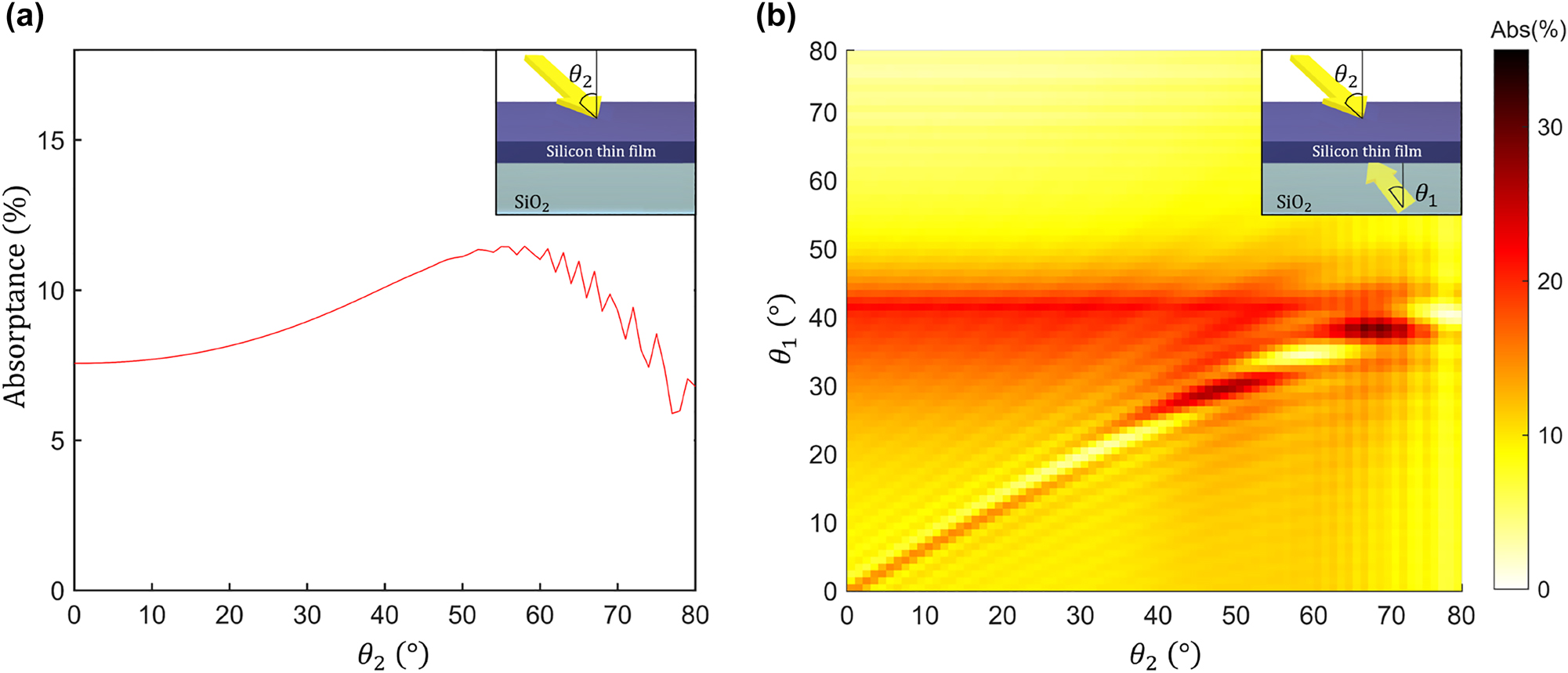
The silicon layer absorptance as the function of the incidence angle under illumination with either a single or two interfering plane waves with angles of incidence θ 1 and θ 2, each varying from 0° to 80°. (a) The angle-dependent absorptance of a single plane wave propagating from the top side. (b) Two plane waves incident on the absorber from opposite directions yield absorptance characteristics that are highly sensitive to small changes in their incidence angles. This effect can be used to design an optical angular sensor, where we fix the incidence angle of one wave and use the other wave as a probe. The inset figures indicate the incidence angles and the 1D geometry used in the simulations.

The silicon film absorptance as a function of the incidence angle of the bottom plane wave (θ 1), while the incidence angle of the plane wave at the top (θ 2) is fixed at 57°. The inset shows a 1D structure used in the simulations. The minimum absorptance of 3.67 % (indicated as the blue circle) occurs at an incidence angle of 34° with the phase difference of 35.58° between incidence waves within the silicon film. In contrast, a 3.0° shift of the incidence angle away from θ 1,tar generates multiple OVs in the 750 nm thick silicon layer, resulting in a 6.05-fold absorptance enhancement.
To reveal the correlation between the enhancement and suppression of the thin film absorptance observed in Figure 3 and the generation and annihilation of OVs in the absorber near field, we calculate and plot in Figure 4 the spatial distributions of the magnitude and direction of the Poynting vector of the two-wave interference field at the wavelengths corresponding to Max1, Max2, Max, and Min points. The time-averaged Poynting vector can be calculated with the following equation:
where

Magnitude
In turn,
Here, the value of Γ(x, y) at each point in space x, y is calculated by integrating a scalar product of the Poynting vector and a unit vector
Figure 4 shows the magnitude and the direction of the Poynting vector as well as the new power flow circulation parameter (Γ(x, y)) in the near field of the 750 nm thick silicon film for each scenario (Max1, Max2, Min, and Max) indicated in Figure 3. The images in the insets of Figure 4(a), (c), and (g) illustrate how destructive interference of two plane waves creates multiple OVs within the silicon layer, translating into greater absorptance. In comparison, as shown in Figure 4(e), constructive interference of two opposite plane waves generates a typical periodic intensity pattern but does not lead to the formation of OVs and, counter-intuitively, leads to low absorptance (3.67 % in the Min case). On the other hand, the optimum absorptance (22.20 %), depicted in Figure 4(g) and (h), is driven by strong local circulatory optical power flow in the form of seven pairs of counterclockwise (+) and clockwise (−) OVs, which are characterized by high values of Γ(x, y). In turn, the optical interference field corresponding to the other local absorption maxima, depicted in Figure 4(a)–(d), (18.00 %, 17.64 %) also feature multiple OV pairs, which, however, have lower circulation parameter values as compared to the Max case. These results confirm that the formation of real-space OVs underlies the absorption spectral features in thin films, and the circulation parameter can serve as a good measure for the resonant absorptance enhancement. The maximum OV circularity in Figure 4(g) is 24.04 %.
Figure 5 shows simulated absorptance spectra for two different incidence angles (corresponding to the cases labeled as θ Min = 34° and θ Max = 41° in Figure 3). At the wavelength of 775 nm, the probe plane wave arriving from the bottom at 41° interferes with the downward-propagating plane wave, creating OVs and yielding a total absorptance of 22.20 %. In contrast, the interference of the two waves when the probe wave arrives at the angle of 34° yields only 3.67 % absorptance. The contrast absorptance ratio at 775 nm is 6.05, while a similar high-contrast absorptance ratio is observed as 4.57 at the wavelength of 630 nm. When the incidence angle (θ 1) of the probe plane wave is 41°, the full-width-half-maximum (FWHM) is estimated as 21 nm at the 630 nm wavelength. The high-absorptance-contrast wavelength position and width can further be tuned to overlap with a specific laser emission spectrum by the judicious choice of absorber thickness. Both angular and wavelength sensitivity of the absorptance to the probe wave parameters, which are underlied by the OV generation in the interference field, can be leveraged to design angle-sensitive detectors [55, 57], wavelength-sensitive detectors [57–60], and color filters [61].
![Figure 5:
Absorptance spectra of the same planar structure as in Figures 3 and 4 over the wavelength range from 600 to 800 nm for the two angles of incidence of the upward-propagating probe wave corresponding to the Min and Max cases. The blue curve represents the Min (θ
1 = 34°), and the red curve represents the Max (θ
1 = 41°) case, while the downward-propagating plane wave arrives at an angle of θ
2 = 57°. The absorptance contrast ratio between Min and Max is maximized at the wavelengths of 775 nm (shown in Figures 3 and 4) and 630 nm. The absorptance peak at 630 nm exhibits a relatively narrow FWHM (21 nm), which could be leveraged for the design of a wavelength-selective and angle-selective sensor [56].](/document/doi/10.1515/nanoph-2023-0583/asset/graphic/j_nanoph-2023-0583_fig_005.jpg)
Absorptance spectra of the same planar structure as in Figures 3 and 4 over the wavelength range from 600 to 800 nm for the two angles of incidence of the upward-propagating probe wave corresponding to the Min and Max cases. The blue curve represents the Min (θ 1 = 34°), and the red curve represents the Max (θ 1 = 41°) case, while the downward-propagating plane wave arrives at an angle of θ 2 = 57°. The absorptance contrast ratio between Min and Max is maximized at the wavelengths of 775 nm (shown in Figures 3 and 4) and 630 nm. The absorptance peak at 630 nm exhibits a relatively narrow FWHM (21 nm), which could be leveraged for the design of a wavelength-selective and angle-selective sensor [56].
However, while this approach enables efficient absorption suppression at the Min point, the level of absorptance at the maximum absorption points is only around 20 % due to the lack of effective design parameters. Furthermore, aligning the two beams and precisely controlling their phases could still be challenging. These limitations require a new approach for further analysis. Therefore, in the following sections, we consider the case of a single wave incidence, and instead of interfering two waves, we optimize the absorptance in a thin silicon film by engineering nano-structured metasurface coatings made from lossless dielectrics [27] using the inverse design method [62–64]. This allows us to demonstrate a dramatic absorption enhancement in a much thinner silicon absorber (100 nm thick). As we show in the following, our design approach allows achieving perfect absorption in subwavelength-thick films by decoupling the photon and electron propagating lengths in composite absorber structures, which should further lead to increased performance of infrared detectors [65].
3 Inverse design of ultrathin perfect absorbers
Adjoint optimization, one of inverse design methods, enables large-scale optimization of photonic structures, such as metalenses [41, 66], [67], [68], solar cells [40–42], bio-sensors [27, 45], and OV beam emitters [36, 48]. The adjoint optimization algorithm is based on calculating derivatives of the chosen figure of merit (FoM) induced by the change of the permittivity δFoM/δϵ(x) with only two simulation runs (a direct and an adjoint simulation). Specifically, a slight change of the permittivity in the designable region can be approximated as a superposition of a simulation with no change and a simulation with a dipole excitation at the location of the permittivity change. Then, the Lorentz reciprocity principle is used to replace many simulations of dipoles at different positions within the designable region with a single dipole simulation at the detector location [40]. This process simplifies the calculation of derivatives of FoM with respect to the change of permittivities (δFoM/δϵ(x)) with the dot product of electric field (E Dir ) from the incidence wave and the adjoint field (E Adj ) from the dipole source. The back-propagating field of the adjoint source is given by J Adj = −iω P = −iω(δFoM/δ E), where P is a polarization density. This technique enables us to solve complicated photonic problems with many design parameters within feasible computational time.
Prior studies indicate that a combination of periodicity and randomness in the absorber surface design is vital to achieving greater absorptance in dielectric thin films [42, 69]. In this work, we employ a metasurface design periodicity of 1.5 μm and define FoM as the maximum of electric field intensity (|E(x 0, y 0)|2) at the center of 100 nm thick silicon film at a 775 nm wavelength. We have tested multiple field-maximization points and different FoMs, and our results demonstrate that maximizing the field intensity at a well-chosen periodic distance (1.5 μm) can yield a design exhibiting a perfect absorption in the 100 nm thick silicon film. We employ Meep FDTD [51] combined with a pre-qualified in-house adjoint optimization algorithm [27, 68]. The resolution of FDTD simulation is 60 (pixels/μm), which decides the pixel size of the simulation.
Figure 6 shows a schematic illustrating a design of a structure achieving perfect absorption in a planar silicon thin film driven by the OV generation in the interference near-field, which is optimized through the inverse design method. We consider a 100 nm thick silicon layer on a glass substrate illuminated with a 775 nm-wavelength plane wave. At this wavelength, silicon has a low absorption coefficient of 1.10 × 10³ (cm−1) [70], resulting in 3.67 % single-pass absorptance in a planar layer. The designable region consisting of TiO2 layer is placed above the silicon film. We first use the adjoint optimization process to optimize the geometry of the TiO2 layer (as a free-form metasurface) and then apply additional minimum feature size constraints to obtain a lithography-compatible grating-type structure. The optimized TiO2 layer creates a desired reflection of incidence wave at the layer interface, leading to an OV generation within a silicon thin film. However, it does not necessarily have a TiO2 layer for creating multiple OVs, whereas many other materials can be applied to an inverse design of perfect absorption. We chose TiO2 due to its relatively high refractive index and zero absorptivity at the visible wavelength.

Schematic of the inverse design problem. Through adjoint optimization, we optimize the TiO2 layer geometry to maximize the OV-driven absorptance in a 100 nm thick silicon film under the illumination with a plane wave incident at the absorber from the glass layer side at angle θ 1,tar . Multiple OV pairs form within the thin film at frequencies corresponding to the perfect absorption condition. The side surface plot (accompanied by the color bar and the arrow on the right-hand side) shows the Poynting vector phase distribution (ϕ s ) within the silicon film defined by Eq. (2).
First, we optimize the designable region with a free-form TiO2 metasurface geometry. In this simulation, the minimum feature size of the designable region is the same as the simulation grid spacing, and the density of TiO2 is allowed to vary between 0 and 1 at every location in the designable region, known as the topology optimization approach. Then, penalty functions [71] are added to the FoM function to impose a binary-material constraint (ultimately, allowing only 0 and 1 density values of material at each location).
Later in this section, we also impose the restriction of constant material density in the z-direction, which ensures the structure manufacturability via traditional lithography methods [72]. The initial density parameters are selected randomly within a range of 0.45–0.55. The free-form-based optimization can provide insight regarding a computational upper limit of the FoM for the given optimization problem [73, 74]. A free-form design can have numerous degrees of freedom depending on the grid spacing chosen for a simulation. Therefore, an optimized free-form structure can potentially yield a design with the FoM reaching a physical bound of a given structure [73].
Figure 7(a) shows several inverse design iterations exhibiting progressively increasing values of the normalized FoM. At the initial iterations, adjoint derivatives with respect to the change of permittivity (δFoM/δϵ(x)) dominate the optimization process. Then, the penalization factor converts grayscale permittivity values to binarized permittivity values (corresponding to those of TiO2 and air). The penalization factor gradually increases over the inverse design iteration until the design parameters are fully binarized, as shown in the red inset figure in Figure 7(a). Figure 7(b) shows the absorptance of the structure as a function of the plane wave incidence angle. The inverse-designed structure exhibits perfect absorption (99.90 %) at the target incidence angle (−45°, 45°). It is a 19.44-fold enhancement compared to the single-pass absorptance at the target angle, as shown with the blue curve in Figure 7(b). Figure 8(a) illustrates the optical power flow patterns inside the optimized inverse-designed free-form TiO2 geometry under the illumination with a plane wave at a 45° incidence angle. The OV pairs formed near the thin film silicon absorber are revealed in Figure 8(b) by plotting the equi-phase lines (ϕ
s
= const) overlaid on top of the heat map showing the magnitude of the Poynting vector
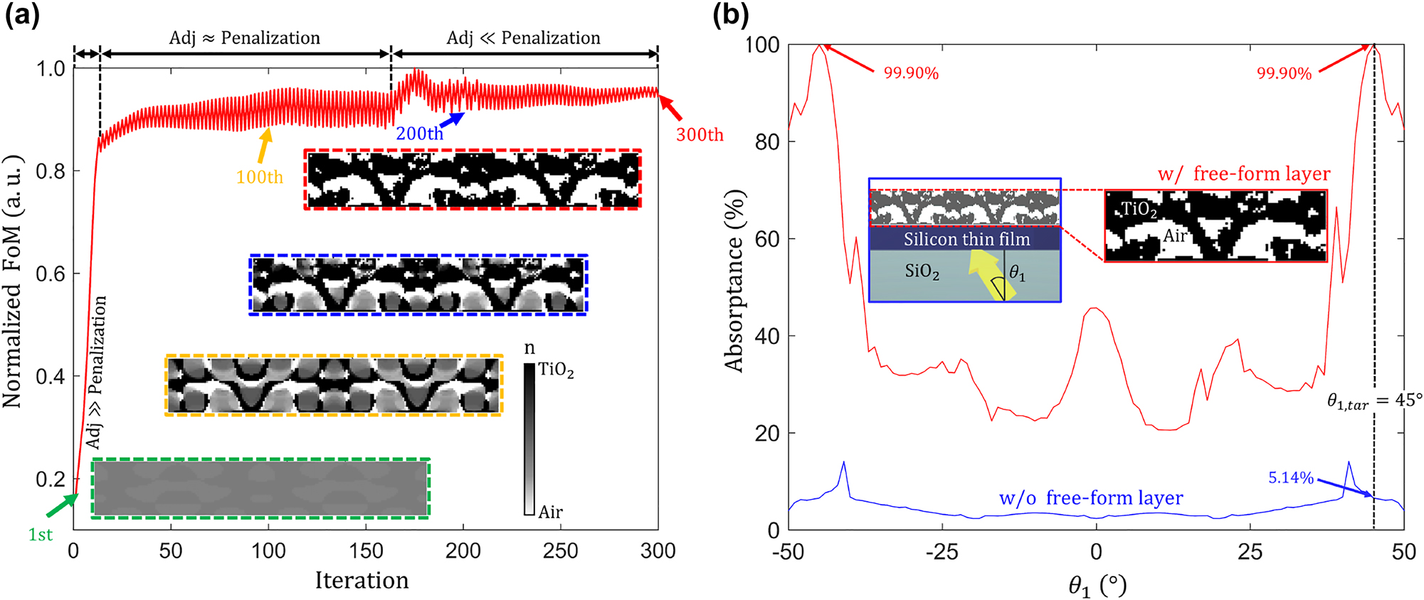
Inverse design procedure for optimizing a TiO2 free-form structure. (a) The FoM is defined as the maximum of the electric field intensity at the center of the thin film when a 775 nm-wavelength s-polarized plane wave is incident at the target angle (θ 1,tar = 45°). The red curve indicates the evolution of the FoM, while the four insets show the changes in the design parameters, where the pixel size is the same as the simulation. The penalization factor gradually increases with the iteration number. Then it starts to exceed the gradients of FoM after the 144th iteration, which enforces grayscale design parameters to be binarized to TiO2 and air. (b) Absorptance of the inverse-designed structure as a function of the incidence angle of the plane wave (θ 1). The blue curve represents the single-pass absorptance, and the red curve corresponds to the absorptance of the inverse-designed structure, which shows perfect absorption (99.90 %) at θ 1 = 45°. This constitutes a 19.44-fold absorptance improvement compared to the single-pass absorptance at the same angle of incidence. The inset figure shows an optimized structure and its surrounding materials.

OV generation inside the inverse-designed TiO2 free-form structure at the perfect absorption. (a) The geometry of the optimized free-form TiO2 structure with a 100 nm thick silicon absorber layer and a SiO2 substrate. The design periodicity is chosen as 1.5 μm, and the plane wave is incident a 45° angle. The optimized design shows 99.90 % absorptance, which is a 19.44-fold improvement compared to the absorptance of a planar 100 nm thick silicon film on SiO2 substrate illuminated with a plane wave at the same incidence angle and frequency. (b) The phase ϕ
s
(x, y) and the magnitude
In this work, we cap the maximum allowed grating height at 500 nm, while the minimum width of the smallest grating feature is capped at 50 nm, which together leads to an aspect ratio of 10. Such 2D TiO2 gratings on SiO2 substrates can be fabricated by electron beam lithography [68, 72, 75, 76] and nanoimprint lithography [77–79]. The inverse design of the grating structure starts with defining grayscale permittivity values in the designable region, as shown in the inset enclosed by the green dashed line in Figure 9(a). The permittivities of the designable region gradually evolve to achieve greater FoM. Once the FoM saturates, grayscale permittivities are reduced to the binary values, corresponding to either TiO2 or air. As discussed previously, the penalization factor gradually increases over the inverse design iteration until the design parameters are fully binarized, as shown in a red inset in Figure 9(a). Figure 9(b) shows the absorptance as a function of the incidence angle. The inverse-designed TiO2 grating enables perfect absorption (97.85 %) in the planar silicon film at the target incidence angle (0°). 97.85 % absorptance constitutes an 18-fold enhancement as compared to the single-pass absorptance at the target angle (see blue curve in Figure 9(b)). While the free-form-based optimization converged to a structure with the optimum FoM, experimental realization of the 2D free-form structure shown in Figure 8(a) is hardly feasible. Thus, to design a structure that can be manufactured by conventional lithographic techniques, we constrain our designable region to a 2D grating structure featuring a translational symmetry in the direction perpendicular to its cross-sectional view.

Inverse design procedure for optimizing a TiO2 grating. (a) Normalized FoM values versus the inverse design iteration number. The red curve illustrates the evolution of the FoM, while the four subplots show the corresponding changes in the design parameters. Initially, the penalization factor gradually increases with the increased number of iterations. Eventually, it exceeds the gradients of FoM after the 90th iteration, which enforces grayscale design parameters to be binarized to TiO2 and air. The four subplots show the changes in the design parameters, where the aspect ratio of the design parameter is 10. (b) The absorptance as a function of the incidence angle of the plane wave (θ 1). The blue curve represents the single-pass absorptance (without grating). The red curve indicates the absorptance of the inverse-designed grating structure, which shows perfect absorption (97.85 %) at θ 1,tar = 0°. This constitutes an 18-fold absorptance improvement compared to the single-pass absorptance level. The inset figure shows the optimized grating metasurface structure on top of the planar silicon absorber and a glass substrate.
Figure 10(a) shows the optimum inverse-designed TiO2 grating geometry that achieves perfect absorption under normal incidence. The OV profiles near the thin film absorber layer are shown in Figure 10(b), where the equi-phase lines (ϕ
s
= const) are plotted on top of the heat map of the magnitude of the Poynting vector

OV generation in the optimum inverse-designed TiO2 grating structure. (a) The optimized grating TiO2 structure with a 100 nm thick silicon absorber layer and a SiO2 substrate. The design periodicity is chosen as 1.5 μm, and the incident plane wave arrives normal to the interface (i.e., at a 0° angle). The optimized design exhibits 97.85 % absorptance, which is an 18-fold improvement over that of a bare planar 100 nm thick silicon layer on a SiO2 substrate. (b) The phase ϕ
s
(x, y) and the magnitude
Both 2D free-form and 2D grating structures exhibit more than 3.53-fold improvement in the OV circularity values compared to the simple 1D structure shown in Figure 4. This demonstrates the correlation between absorption enhancement and high-circularity localized OV fields and also implies that the inverse design can provide a useful numerical tool for generating OV-rich circulating optical fields for photonic applications. In this work, we demonstrated the optimized structures for 45° and 0° incidence angles. In addition, we also optimized for arbitrary incidence angles. For example, the optimized structures for 16° and 42° degree incidence wave show 98.95 % and 94.96 % absorptance, respectively. Although we focus on maximizing field intensity in the thin film at a single frequency and a single incidence angle in this work, our method can be extended to broad-band wide-angle perfect absorption or narrow-band angle-sensitive perfect absorption with a little tweak on the definition of figure of merits. For example, FoM = ∑ λ,θ |E(λ, θ)|2 may leads to a broad-band wide-angle perfect absorption while FoM = |E(λ c , θ c )|2 − ∑ λ,θ |E(λ, θ)|2 can be applicable to narrow-band angle-sensitive perfect absorption, where λ c is a target wavelength and θ c is a target angle. We compare the performance of the inverse-designed OV-based perfect absorber structures with those from prior works, as shown in Figure 11. Absorption enhancement depends on (1) the absorber’s refractive index (with the maximum enhancement factor of 4n 2 known as the Yablonovitch’s limit) [82] (2) absorptivity (i.e., the imaginary part of dielectric permittivity), of the material, and (3) the wavelength-normalized absorber thickness. Therefore, we define normalized design factor (F) as F = dnk/λ, where d is the thickness of the absorber, λ is the wavelength of the incident plane wave, n and k are the real and imaginary parts of the absorber refractive index, respectively [53, 89], [90], [91]. In Figure 11, previously proposed ultrathin absorbers are ranked, including structures with gold [83, 84], MoS2 [85], silicon [55, 86], graphene [87], InSb [53], and GaAs [88] active layers. Our absorber designs (both the free-form and the grating structures) exhibit perfect absorption despite the challenging normalized design factor. In our designs, a 100 nm thick planar silicon absorber layer is characterized by the refractive index and absorptivity values n = 3.714, k = 0.008 at 775 nm wavelength [53], and the wavelength-normalized thickness of 0.129. The inverse-designed free-form structure exhibits 99.90 % absorptance (red dot in Figure 11), and the inverse-designed grating structure exhibits 97.85 % absorptance (blue dot in Figure 11). Both designs have a challenging normalized design factor but achieve perfect absorption through near-field OV generation.
![Figure 11:
Comparison between this work (free-form and grating) and existing works. The normalized design factor is defined as the multiplication of the material thickness ‘d’ and real ‘n’ and imaginary ‘k’ parts of the refractive index divided by the design wavelength ‘λ’. The ‘d/λ’ factor indicates the effective thickness and the imaginary part of the refractive index is highly effective in material absorption. The real part of the refractive index affects the upper limit of the absorption enhancement based on ray-optics limit [42, 82]. The existing studies regarding thin film absorption include gold [83, 84], MoS2 [85], silicon [55, 86], graphene [87], InSb [53], and GaAs [88]. Our designs (free-form, grating) show perfect absorption despite the challenging normalized design factor.](/document/doi/10.1515/nanoph-2023-0583/asset/graphic/j_nanoph-2023-0583_fig_011.jpg)
Comparison between this work (free-form and grating) and existing works. The normalized design factor is defined as the multiplication of the material thickness ‘d’ and real ‘n’ and imaginary ‘k’ parts of the refractive index divided by the design wavelength ‘λ’. The ‘d/λ’ factor indicates the effective thickness and the imaginary part of the refractive index is highly effective in material absorption. The real part of the refractive index affects the upper limit of the absorption enhancement based on ray-optics limit [42, 82]. The existing studies regarding thin film absorption include gold [83, 84], MoS2 [85], silicon [55, 86], graphene [87], InSb [53], and GaAs [88]. Our designs (free-form, grating) show perfect absorption despite the challenging normalized design factor.
4 Conclusions
We have demonstrated the correlation between optical vortices (OVs) and absorption enhancement within planar silicon films. Two types of photonic structures have been introduced: a one-dimensional (1D) planar absorber simultaneously illuminated with two incident plane waves at different angles and an inverse-designed two-dimensional (2D) structure illuminated with a single plane wave.
The former elicits a nearly 4.8-fold absorption enhancement via generation/annihilation of OVs, even with a slight variation (±3° with reference to θ 1 = 34°) of the incidence angle. This finding shows that absorption enhancement can be achieved by the manipulation of OV and can open new opportunities for engineering angle-sensitive or wavelength-sensitive photodetectors.
For the latter, we have achieved perfect absorption in the ultrathin film by maximizing the electric field intensity through adjoint optimization. OVs and the resulting light re-circulations are generated from light interference on the optimized dielectric metasurface placed on top of the planar absorber. The inverse-designed free-form TiO2 structure enables 99.90 % absorptance in a 100 nm thick silicon layer at 775 nm wavelength. This is a 19.44-fold absorptance enhancement compared to a single-pass absorption case. We have further simplified the dielectric metasurface geometry to a grating structure that can be fabricated by standard lithographic or nanoimprint techniques. The inverse-designed TiO2 grating structure enables 97.85 % absorptance in the underlying planar silicon film, which is an 18-fold improvement over the single-pass case. The OV circularities of optimized structures are a maximum of 95.37 % (free-form) and 96.14 % (grating), and their averages are 88.18 % (free-form) and 89.51 % (grating). Our high OV circularity leads to efficient power flow circulation within the absorber, which in turn leads to dramatic absorption enhancement.
Our work confirms the recent finding that perfect absorption is topological in nature [20] and reveals that it is accompanied by the generation/annihilation of real-space OVs as well as OVs in the reciprocal (or generalized parameter) space as previously predicted [22–25].
Funding source: Korea Semiconductor Research Consortium
Award Identifier / Grant number: 20019357
Funding source: Korea Evaluation Institute of Industrial Technology
Award Identifier / Grant number: 1415180303
Award Identifier / Grant number: IITP-(2023)-RS-2023-00253914
Award Identifier / Grant number: IITP-2022-0-0154896
Award Identifier / Grant number: 2020-0-01373
Funding source: Ministry of Science and ICT, South Korea
Award Identifier / Grant number: RS-2023-00261368
Funding source: National Research Foundation of Korea
Award Identifier / Grant number: NRF-2022K1A3A1A91093776
-
Research funding: This work was supported by the High-Potential Individuals Global Training Program (IITP-2022-0-0154896) and Artificial Intelligence Graduate School Program (No. 2020-0-01373, Hanyang University) supervised by the IITP (Institute for Information and Communications Technology Planning and Evaluation), and also supported by the MOTIE (Ministry of Trade, Industry & Energy) 1415180303 and KSRC (Korea Semiconductor Research Consortium) 20019357 support program for the development of the future semiconductor device. This work was supported by IITP under the artificial intelligence semiconductor support program to nurture the best talents (IITP-(2023)-RS-2023-00253914) grant funded by the Korea government (MSIT) and also by the Korea government (MSIT) (RS-2023-00261368), and by National Research Foundation of Korea (NRF-2022K1A3A1A91093776).
-
Author contributions: All authors have accepted responsibility for the entire content of this manuscript and approved its submission.
-
Conflict of interest: The authors state no conflicts of interest.
-
Informed consent: Informed consent was obtained from all individuals included in this study.
-
Ethical approval: The conducted research is not related to either human or animal use.
-
Data availability: The datasets generated and analyzed during the current study are available from the corresponding author upon reasonable request.
References
[1] M. R. Dennis, K. O’holleran, and M. J. Padgett, “Singular optics: optical vortices and polarization singularities,” Prog. Opt., vol. 53, pp. 293–363, 2009.10.1016/S0079-6638(08)00205-9Suche in Google Scholar
[2] M. Soskin, S. V. Boriskina, Y. Chong, M. R. Dennis, and A. Desyatnikov, “Singular optics and topological photonics,” J. Opt., vol. 19, no. 1, p. 010401, 2016. https://doi.org/10.1088/2040-8986/19/1/010401.Suche in Google Scholar
[3] G. C. Berkhout and M. W. Beijersbergen, “Method for probing the orbital angular momentum of optical vortices in electromagnetic waves from astronomical objects,” Phys. Rev. Lett., vol. 101, no. 10, p. 100801, 2008. https://doi.org/10.1103/physrevlett.101.100801.Suche in Google Scholar
[4] A. Bekshaev, K. Y. Bliokh, and M. Soskin, “Internal flows and energy circulation in light beams,” J. Opt., vol. 13, no. 5, p. 053001, 2011. https://doi.org/10.1088/2040-8978/13/5/053001.Suche in Google Scholar
[5] F. Yue, D. Wen, J. Xin, B. D. Gerardot, J. Li, and X. Chen, “Vector vortex beam generation with a single plasmonic metasurface,” ACS Photonics, vol. 3, no. 9, pp. 1558–1563, 2016. https://doi.org/10.1021/acsphotonics.6b00392.Suche in Google Scholar
[6] C. Huang, C. Zhang, S. Xiao, et al.., “Ultrafast control of vortex microlasers,” Science, vol. 367, no. 6481, pp. 1018–1021, 2020. https://doi.org/10.1126/science.aba4597.Suche in Google Scholar PubMed
[7] S. V. Boriskina and B. M. Reinhard, “Molding the flow of light on the nanoscale: from vortex nanogears to phase-operated plasmonic machinery,” Nanoscale, vol. 4, no. 1, pp. 76–90, 2012. https://doi.org/10.1039/c1nr11406a.Suche in Google Scholar PubMed PubMed Central
[8] W. Ahn, S. V. Boriskina, Y. Hong, and B. M. Reinhard, “Electromagnetic field enhancement and spectrum shaping through plasmonically integrated optical vortices,” Nano Lett., vol. 12, no. 1, pp. 219–227, 2012. https://doi.org/10.1021/nl203365y.Suche in Google Scholar PubMed PubMed Central
[9] M. Berry, “Optical vortices evolving from helicoidal integer and fractional phase steps,” J. Opt. A: Pure Appl. Opt., vol. 6, no. 2, p. 259, 2004. https://doi.org/10.1088/1464-4258/6/2/018.Suche in Google Scholar
[10] V. Kotlyar, A. Kovalev, A. Nalimov, and A. Porfirev, “Evolution of an optical vortex with an initial fractional topological charge,” Phys. Rev. A, vol. 102, no. 2, p. 023516, 2020. https://doi.org/10.1103/physreva.102.023516.Suche in Google Scholar
[11] P. Z. Dashti, F. Alhassen, and H. P. Lee, “Observation of orbital angular momentum transfer between acoustic and optical vortices in optical fiber,” Phys. Rev. Lett., vol. 96, no. 4, p. 043604, 2006. https://doi.org/10.1103/physrevlett.96.043604.Suche in Google Scholar PubMed
[12] S. Ramachandran and P. Kristensen, “Optical vortices in fiber,” Nanophotonics, vol. 2, nos. 5–6, pp. 455–474, 2013. https://doi.org/10.1515/nanoph-2013-0047.Suche in Google Scholar
[13] T. Lei, M. Zhang, Y. Li, et al.., “Massive individual orbital angular momentum channels for multiplexing enabled by dammann gratings,” Light: Sci. Appl., vol. 4, no. 3, pp. e257, 2015. https://doi.org/10.1038/lsa.2015.30.Suche in Google Scholar
[14] K. V. Sreekanth, S. Sreejith, S. Han, et al.., “Biosensing with the singular phase of an ultrathin metal-dielectric nanophotonic cavity,” Nat. Commun., vol. 9, no. 1, p. 369, 2018. https://doi.org/10.1038/s41467-018-02860-6.Suche in Google Scholar PubMed PubMed Central
[15] C. Prajapati and N. K. Viswanathan, “Observation of diffractive-correction and spin-orbit interaction induced effects around the brewster angle,” J. Opt., vol. 21, no. 8, p. 084002, 2019. https://doi.org/10.1088/2040-8986/ab2d55.Suche in Google Scholar
[16] M. Weber, M. Leutenegger, S. Stoldt, et al.., “Minsted fluorescence localization and nanoscopy,” Nat. Photonics, vol. 15, no. 5, pp. 361–366, 2021. https://doi.org/10.1038/s41566-021-00774-2.Suche in Google Scholar PubMed PubMed Central
[17] H. Rubinsztein-Dunlop, A. Forbes, M. V. Berry, et al.., “Roadmap on structured light,” J. Opt., vol. 19, no. 1, p. 013001, 2016. https://doi.org/10.1088/2040-8978/19/1/013001.Suche in Google Scholar
[18] A. M. Yao and M. J. Padgett, “Orbital angular momentum: origins, behavior and applications,” Adv. Opt. Photonics, vol. 3, no. 2, pp. 161–204, 2011. https://doi.org/10.1364/aop.3.000161.Suche in Google Scholar
[19] V. Kravets, F. Schedin, R. Jalil, et al.., “Singular phase nano-optics in plasmonic metamaterials for label-free single-molecule detection,” Nat. Mater., vol. 12, no. 4, pp. 304–309, 2013. https://doi.org/10.1038/nmat3537.Suche in Google Scholar PubMed
[20] Y. Tsurimaki, J. K. Tong, V. N. Boriskin, et al.., “Topological engineering of interfacial optical tamm states for highly sensitive near-singular-phase optical detection,” ACS Photonics, vol. 5, no. 3, pp. 929–938, 2018. https://doi.org/10.1021/acsphotonics.7b01176.Suche in Google Scholar
[21] V. Lucarini, J. J. Saarinen, K.-E. Peiponen, and E. M. Vartiainen, Kramers-Kronig Relations in Optical Materials Research, vol. 110, Heidelberg, Germany, Springer Science & Business Media, 2005.Suche in Google Scholar
[22] M. Liu, W. Chen, G. Hu, et al.., “Spectral phase singularity and topological behavior in perfect absorption,” Phys. Rev. B, vol. 107, no. 24, p. L241403, 2023. https://doi.org/10.1103/physrevb.107.l241403.Suche in Google Scholar
[23] Z. Sakotic, A. Krasnok, A. Alú, and N. Jankovic, “Topological scattering singularities and embedded eigenstates for polarization control and sensing applications,” Photonics Res., vol. 9, no. 7, pp. 1310–1323, 2021. https://doi.org/10.1364/prj.424247.Suche in Google Scholar
[24] Y. Guo, M. Xiao, and S. Fan, “Topologically protected complete polarization conversion,” Phys. Rev. Lett., vol. 119, no. 16, p. 167401, 2017. https://doi.org/10.1103/physrevlett.119.167401.Suche in Google Scholar
[25] A. Berkhout and A. F. Koenderink, “Perfect absorption and phase singularities in plasmon antenna array etalons,” ACS Photonics, vol. 6, no. 11, pp. 2917–2925, 2019. https://doi.org/10.1021/acsphotonics.9b01019.Suche in Google Scholar
[26] S. Boriskina and N. I. Zheludev, Singular and Chiral Nanoplasmonics, New York, NY, CRC Press, 2014.10.1201/b17632Suche in Google Scholar
[27] H. Chung and S. V. Boriskina, “Inverse design of a single-frequency diffractive biosensor based on the reporter cleavage detection mechanism,” Opt. Express, vol. 29, no. 7, pp. 10780–10799, 2021. https://doi.org/10.1364/oe.421656.Suche in Google Scholar
[28] S. V. Boriskina and B. M. Reinhard, “Adaptive on-chip control of nano-optical fields with optoplasmonic vortex nanogates,” Opt. Express, vol. 19, no. 22, pp. 22305–22315, 2011. https://doi.org/10.1364/oe.19.022305.Suche in Google Scholar PubMed PubMed Central
[29] H. Wolter, “Concerning the path of light upon total reflection,” J. Opt. A: Pure Appl. Opt., vol. 11, no. 9, p. 090401, 2009. https://doi.org/10.1088/1464-4258/11/9/090401.Suche in Google Scholar
[30] V. Lembessis, M. Babiker, and D. Andrews, “Surface optical vortices,” Phys. Rev. A, vol. 79, no. 1, p. 011806, 2009. https://doi.org/10.1103/physreva.79.011806.Suche in Google Scholar
[31] M. R. Dennis and J. B. Götte, “Topological aberration of optical vortex beams: determining dielectric interfaces by optical singularity shifts,” Phys. Rev. Lett., vol. 109, no. 18, p. 183903, 2012. https://doi.org/10.1103/physrevlett.109.183903.Suche in Google Scholar PubMed
[32] D. Kim, A. Baucour, Y.-S. Choi, J. Shin, and M.-K. Seo, “Spontaneous generation and active manipulation of real-space optical vortices,” Nature, vol. 611, no. 7934, pp. 48–54, 2022. https://doi.org/10.1038/s41586-022-05229-4.Suche in Google Scholar PubMed
[33] Z. Wang, N. Zhang, and X.-C. Yuan, “High-volume optical vortex multiplexing and de-multiplexing for free-space optical communication,” Opt. Express, vol. 19, no. 2, pp. 482–492, 2011. https://doi.org/10.1364/oe.19.000482.Suche in Google Scholar
[34] Z. Xie, T. Lei, F. Li, et al.., “Ultra-broadband on-chip twisted light emitter for optical communications,” Light: Sci. Appl., vol. 7, no. 4, pp. 18001, 2018. https://doi.org/10.1038/lsa.2018.1.Suche in Google Scholar PubMed PubMed Central
[35] Y. Liu, W. Chen, W. Zhang, et al.., “Visible and online detection of near-infrared optical vortices via nonlinear photonic crystals,” Adv. Opt. Mater., vol. 10, no. 1, p. 2101098, 2022. https://doi.org/10.1002/adom.202101098.Suche in Google Scholar
[36] A. D. White, L. Su, D. I. Shahar, et al.., “Inverse design of optical vortex beam emitters,” ACS Photonics, vol. 10, no. 4, pp. 803–807, 2023.10.1021/acsphotonics.2c01007Suche in Google Scholar
[37] K. E. Chong, I. Staude, A. James, et al.., “Polarization-independent silicon metadevices for efficient optical wavefront control,” Nano Lett., vol. 15, no. 8, pp. 5369–5374, 2015. https://doi.org/10.1021/acs.nanolett.5b01752.Suche in Google Scholar PubMed
[38] P. Genevet and F. Capasso, “Holographic optical metasurfaces: a review of current progress,” Rep. Prog. Phys., vol. 78, no. 2, p. 024401, 2015. https://doi.org/10.1088/0034-4885/78/2/024401.Suche in Google Scholar PubMed
[39] H. Sroor, Y.-W. Huang, B. Sephton, et al.., “High-purity orbital angular momentum states from a visible metasurface laser,” Nat. Photonics, vol. 14, no. 8, pp. 498–503, 2020. https://doi.org/10.1038/s41566-020-0623-z.Suche in Google Scholar
[40] O. D. Miller, Photonic Design: From Fundamental Solar Cell Physics to Computational Inverse Design, Berkeley, Dissertation, Dept. Electrical. Eng., University of California, 2012.Suche in Google Scholar
[41] S. Molesky, Z. Lin, A. Y. Piggott, W. Jin, J. Vucković, and A. W. Rodriguez, “Inverse design in nanophotonics,” Nat. Photonics, vol. 12, no. 11, pp. 659–670, 2018. https://doi.org/10.1038/s41566-018-0246-9.Suche in Google Scholar
[42] V. Ganapati, O. D. Miller, and E. Yablonovitch, “Light trapping textures designed by electromagnetic optimization for subwavelength thick solar cells,” IEEE J. Photovolt., vol. 4, no. 1, pp. 175–182, 2013. https://doi.org/10.1109/jphotov.2013.2280340.Suche in Google Scholar
[43] J. Lu, S. Boyd, and J. Vučković, “Inverse design of a three-dimensional nanophotonic resonator,” Opt. Express, vol. 19, no. 11, pp. 10563–10570, 2011. https://doi.org/10.1364/oe.19.010563.Suche in Google Scholar PubMed
[44] D. Høj, F. Wang, W. Gao, U. B. Hoff, O. Sigmund, and U. L. Andersen, “Ultra-coherent nanomechanical resonators based on inverse design,” Nat. Commun., vol. 12, no. 1, p. 5766, 2021. https://doi.org/10.1038/s41467-021-26102-4.Suche in Google Scholar PubMed PubMed Central
[45] H. Chung, J. Park, and S. V. Boriskina, “Inverse-designed waveguide-based biosensor for high-sensitivity, single-frequency detection of biomolecules,” Nanophotonics, vol. 11, no. 7, pp. 1427–1442, 2022. https://doi.org/10.1515/nanoph-2022-0012.Suche in Google Scholar
[46] C. Dory, D. Vercruysse, K. Y. Yang, et al.., “Inverse-designed diamond photonics,” Nat. Commun., vol. 10, no. 1, p. 3309, 2019. https://doi.org/10.1038/s41467-019-11343-1.Suche in Google Scholar PubMed PubMed Central
[47] J. Yang, M. A. Guidry, D. M. Lukin, K. Yang, and J. Vučković, “Inverse-designed silicon carbide quantum and nonlinear photonics,” 2023, arXiv preprint arXiv:2303.17079.10.1364/CLEO_SI.2022.STh4F.4Suche in Google Scholar
[48] E. Otte, A. D. White, N. A. Güsken, J. Vučković, and M. L. Brongersma, “Tunable vector beam decoder by inverse design for high-dimensional quantum key distribution with 3d polarized spatial modes,” 2023, arXiv preprint arXiv:2304.12296.Suche in Google Scholar
[49] J. Faist, F. Capasso, C. Sirtori, K. W. West, and L. Pfeiffer, “Controlling the sign of quantum interference by tunnelling from quantum wells,” Nature, vol. 390, no. 6660, pp. 589–591, 1997. https://doi.org/10.1038/37562.Suche in Google Scholar
[50] S. Davuluri, Y. Wang, and S. Zhu, “Destructive and constructive interference in the coherently driven three-level systems,” J. Mod. Opt., vol. 62, no. 13, pp. 1091–1097, 2015. https://doi.org/10.1080/09500340.2015.1020895.Suche in Google Scholar
[51] A. F. Oskooi, D. Roundy, M. Ibanescu, P. Bermel, J. D. Joannopoulos, and S. G. Johnson, “Meep: a flexible free-software package for electromagnetic simulations by the fdtd method,” Comput. Phys. Commun., vol. 181, no. 3, pp. 687–702, 2010. https://doi.org/10.1016/j.cpc.2009.11.008.Suche in Google Scholar
[52] D. M. Sullivan, Electromagnetic Simulation using the FDTD Method, Hoboken, NJ, John Wiley & Sons, 2013.10.1002/9781118646700Suche in Google Scholar
[53] D. E. Aspnes and A. Studna, “Dielectric functions and optical parameters of si, ge, gap, gaas, gasb, inp, inas, and insb from 1.5 to 6.0 ev,” Phys. Rev. B, vol. 27, no. 2, p. 985, 1983. https://doi.org/10.1103/physrevb.27.985.Suche in Google Scholar
[54] Y. Jing, Z. Li, Q. Li, et al.., “Angular dependence of optical modes in metal-insulator-metal coupled quantum well infrared photodetector,” AIP Adv., vol. 6, no. 4, p. 045205, 2016. https://doi.org/10.1063/1.4947036.Suche in Google Scholar
[55] A. Nagarajan, S. Hara, H. Satoh, A. P. Panchanathan, and H. Inokawa, “Angle-sensitive detector based on silicon-on-insulator photodiode stacked with surface plasmon antenna,” Sensors, vol. 20, no. 19, p. 5543, 2020. https://doi.org/10.3390/s20195543.Suche in Google Scholar PubMed PubMed Central
[56] S. Ogawa, K. Okada, N. Fukushima, and M. Kimata, “Wavelength selective uncooled infrared sensor by plasmonics,” Appl. Phys. Lett., vol. 100, no. 2, p. 021111, 2012. https://doi.org/10.1063/1.3673856.Suche in Google Scholar
[57] Z. Li, Y. Cheng, H. Luo, F. Chen, and X. Li, “Dual-band tunable terahertz perfect absorber based on all-dielectric insb resonator structure for sensing application,” J. Alloys Compd., vol. 925, p. 166617, 2022. https://doi.org/10.1016/j.jallcom.2022.166617.Suche in Google Scholar
[58] J. W. Cleary, R. Soref, and J. R. Hendrickson, “Long-wave infrared tunable thin-film perfect absorber utilizing highly doped silicon-on-sapphire,” Opt. Express, vol. 21, no. 16, pp. 19363–19374, 2013. https://doi.org/10.1364/oe.21.019363.Suche in Google Scholar
[59] K. V. Sreekanth, S. Han, and R. Singh, “Ge2sb2te5-based tunable perfect absorber cavity with phase singularity at visible frequencies,” Adv. Mater., vol. 30, no. 21, p. 1706696, 2018. https://doi.org/10.1002/adma.201706696.Suche in Google Scholar PubMed
[60] F. Wu, D. Liu, and S. Xiao, “Bandwidth-tunable near-infrared perfect absorption of graphene in a compound grating waveguide structure supporting quasi-bound states in the continuum,” Opt. Express, vol. 29, no. 25, pp. 41975–41989, 2021. https://doi.org/10.1364/oe.446270.Suche in Google Scholar
[61] Z. Li, S. Butun, and K. Aydin, “Large-area, lithography-free super absorbers and color filters at visible frequencies using ultrathin metallic films,” ACS Photonics, vol. 2, no. 2, pp. 183–188, 2015. https://doi.org/10.1021/ph500410u.Suche in Google Scholar
[62] R. Pestourie, C. Pérez-Arancibia, Z. Lin, W. Shin, F. Capasso, and S. G. Johnson, “Inverse design of large-area metasurfaces,” Opt. Express, vol. 26, no. 26, pp. 33732–33747, 2018. https://doi.org/10.1364/oe.26.033732.Suche in Google Scholar PubMed
[63] M. Mansouree, H. Kwon, E. Arbabi, A. McClung, A. Faraon, and A. Arbabi, “Multifunctional 2.5 d metastructures enabled by adjoint optimization,” Optica, vol. 7, no. 1, pp. 77–84, 2020. https://doi.org/10.1364/optica.374787.Suche in Google Scholar
[64] Z. Li, R. Pestourie, Z. Lin, S. G. Johnson, and F. Capasso, “Empowering metasurfaces with inverse design: principles and applications,” ACS Photonics, vol. 9, no. 7, pp. 2178–2192, 2022. https://doi.org/10.1021/acsphotonics.1c01850.Suche in Google Scholar
[65] H. A. Atwater and A. Polman, “Plasmonics for improved photovoltaic devices,” Nat. Mater., vol. 9, no. 3, pp. 205–213, 2010. https://doi.org/10.1038/nmat2629.Suche in Google Scholar PubMed
[66] H. Chung and O. D. Miller, “High-na achromatic metalenses by inverse design,” Opt. Express, vol. 28, no. 5, pp. 6945–6965, 2020. https://doi.org/10.1364/oe.385440.Suche in Google Scholar
[67] S. W. D. Lim, M. L. Meretska, and F. Capasso, “A high aspect ratio inverse-designed holey metalens,” Nano Lett., vol. 21, no. 20, pp. 8642–8649, 2021. https://doi.org/10.1021/acs.nanolett.1c02612.Suche in Google Scholar PubMed
[68] H. Chung, F. Zhang, H. Li, O. D. Miller, and H. I. Smith, “Inverse design of high-na metalens for maskless lithography,” Nanophotonics, vol. 12, no. 13, pp. 2371–2381, 2023. https://doi.org/10.1515/nanoph-2022-0761.Suche in Google Scholar
[69] H. Chung, K. Jung, X. Tee, and P. Bermel, “Time domain simulation of tandem silicon solar cells with optimal textured light trapping enabled by the quadratic complex rational function,” Opt. Express, vol. 22, no. 103, pp. A818–A832, 2014. https://doi.org/10.1364/oe.22.00a818.Suche in Google Scholar PubMed
[70] M. A. Green and M. J. Keevers, “Optical properties of intrinsic silicon at 300 k,” Prog. Photovolt.: Res. Appl., vol. 3, no. 3, pp. 189–192, 1995. https://doi.org/10.1002/pip.4670030303.Suche in Google Scholar
[71] M. M. Neves, O. Sigmund, and M. P. Bendsøe, “Topology optimization of periodic microstructures with a penalization of highly localized buckling modes,” Int. J. Numer. Methods Eng., vol. 54, no. 6, pp. 809–834, 2002. https://doi.org/10.1002/nme.449.Suche in Google Scholar
[72] Y. Chen, “Nanofabrication by electron beam lithography and its applications: a review,” Microelectron. Eng., vol. 135, pp. 57–72, 2015. https://doi.org/10.1016/j.mee.2015.02.042.Suche in Google Scholar
[73] H. Shim, H. Chung, and O. D. Miller, “Maximal free-space concentration of electromagnetic waves,” Phys. Rev. Appl., vol. 14, no. 1, p. 014007, 2020. https://doi.org/10.1103/physrevapplied.14.014007.Suche in Google Scholar
[74] H. Chung, “Computational upper-limit of directional light emission in nano-led via inverse design,” Opt. Express, vol. 30, no. 6, pp. 9008–9020, 2022. https://doi.org/10.1364/oe.451008.Suche in Google Scholar
[75] U. D. Zeitner, M. Oliva, F. Fuchs, et al.., “High performance diffraction gratings made by e-beam lithography,” Appl. Phys. A, vol. 109, pp. 789–796, 2012. https://doi.org/10.1007/s00339-012-7346-z.Suche in Google Scholar
[76] K. Li, J. Li, C. Reardon, et al.., “High speed e-beam writing for large area photonic nanostructures—a choice of parameters,” Sci. Rep., vol. 6, no. 1, p. 32945, 2016. https://doi.org/10.1038/srep32945.Suche in Google Scholar PubMed PubMed Central
[77] L. J. Guo, “Nanoimprint lithography: methods and material requirements,” Adv. Mater., vol. 19, no. 4, pp. 495–513, 2007. https://doi.org/10.1002/adma.200600882.Suche in Google Scholar
[78] Y. Chen, “Applications of nanoimprint lithography/hot embossing: a review,” Appl. Phys. A, vol. 121, pp. 451–465, 2015. https://doi.org/10.1007/s00339-015-9071-x.Suche in Google Scholar
[79] Y. Gu, J. Xu, J. Lin, et al.., “The fabrication of anti-reflection grating structures film for solar cells using vibration-assisted uv nanoimprint lithography,” Sol. Energy, vol. 241, pp. 172–183, 2022. https://doi.org/10.1016/j.solener.2022.02.057.Suche in Google Scholar
[80] Y. Wu, X. Xu, C. Zhang, et al.., “Efficient generation of tunable magnetic and optical vortices using plasmas,” Phys. Rev. Res., vol. 5, no. 1, p. L012011, 2023. https://doi.org/10.1103/physrevresearch.5.l012011.Suche in Google Scholar
[81] J. Liu, Y. Cheng, F. Chen, H. Luo, and X. Li, “Tri-band terahertz vortex beam generator based on a completely independent geometric phase metasurface,” JOSA B, vol. 40, no. 2, pp. 441–449, 2023. https://doi.org/10.1364/josab.481099.Suche in Google Scholar
[82] E. Yablonovitch, “Statistical ray optics,” JOSA, vol. 72, no. 7, pp. 899–907, 1982. https://doi.org/10.1364/josa.72.000899.Suche in Google Scholar
[83] N. Liu, M. Mesch, T. Weiss, M. Hentschel, and H. Giessen, “Infrared perfect absorber and its application as plasmonic sensor,” Nano Lett., vol. 10, no. 7, pp. 2342–2348, 2010. https://doi.org/10.1021/nl9041033.Suche in Google Scholar PubMed
[84] T. Roger, S. Vezzoli, E. Bolduc, et al.., “Coherent perfect absorption in deeply subwavelength films in the single-photon regime,” Nat. Commun., vol. 6, no. 1, p. 7031, 2015. https://doi.org/10.1038/ncomms8031.Suche in Google Scholar PubMed PubMed Central
[85] J. R. Piper and S. Fan, “Broadband absorption enhancement in solar cells with an atomically thin active layer,” ACS Photonics, vol. 3, no. 4, pp. 571–577, 2016. https://doi.org/10.1021/acsphotonics.5b00510.Suche in Google Scholar
[86] R. Yang, C. Dai, C. Wan, G. Zheng, and Z. Li, “Planar ultrathin omni-directional perfect absorber utilizing amorphous silicon for photovoltaics,” Opt. Mater. Express, vol. 10, no. 2, pp. 532–539, 2020. https://doi.org/10.1364/ome.382506.Suche in Google Scholar
[87] R. Li, Y. Zheng, Y. Luo, et al.., “Multi-peak narrow-band perfect absorber based on two-dimensional graphene array,” Diamond Relat. Mater., vol. 120, p. 108666, 2021. https://doi.org/10.1016/j.diamond.2021.108666.Suche in Google Scholar
[88] Y. Wang, K. Chen, Y.-S. Lin, and B.-R. Yang, “Plasmonic metasurface with quadrilateral truncated cones for visible perfect absorber,” Phys. E, vol. 139, p. 115140, 2022. https://doi.org/10.1016/j.physe.2022.115140.Suche in Google Scholar
[89] P. B. Johnson and R.-W. Christy, “Optical constants of the noble metals,” Phys. Rev. B, vol. 6, no. 12, p. 4370, 1972. https://doi.org/10.1103/physrevb.6.4370.Suche in Google Scholar
[90] A. Beal and H. Hughes, “Kramers-kronig analysis of the reflectivity spectra of 2h-mos2, 2h-mose2 and 2h-mote2,” J. Phys. C: Solid State Phys., vol. 12, no. 5, p. 881, 1979. https://doi.org/10.1088/0022-3719/12/5/017.Suche in Google Scholar
[91] K. K. Tikuišis, A. Dubroka, K. Uhlířová, et al.., “Dielectric function of epitaxial quasi-freestanding monolayer graphene on si-face 6h-sic in a broad spectral range,” Phys. Rev. Mater., vol. 7, no. 4, p. 044201, 2023. https://doi.org/10.1103/physrevmaterials.7.044201.Suche in Google Scholar
© 2023 the author(s), published by De Gruyter, Berlin/Boston
This work is licensed under the Creative Commons Attribution 4.0 International License.
Artikel in diesem Heft
- Frontmatter
- Research Articles
- Reconfigurable polarization processor based on coherent four-port micro-ring resonator
- Multiplexing in photonics as a resource for optical ternary content-addressable memory functionality
- Fast and accurate electromagnetic field calculation for substrate-supported metasurfaces using the discrete dipole approximation
- Robust reconfigurable radiofrequency photonic filters based on a single silicon in-phase/quadrature modulator
- A low-loss molybdenum plasmonic waveguide: perfect single-crystal preparation and subwavelength grating optimization
- Controlling coherent perfect absorption via long-range connectivity of defects in three-dimensional zero-index media
- Dynamic propagation of an Airy beam in metasurface-enabled gradiently-aligned liquid crystals
- All-dielectric metaoptics for the compact generation of double-ring perfect vector beams
- Reconfigurable nonlinear losses of nanomaterial covered waveguides
- Inverse design and optical vortex manipulation for thin-film absorption enhancement