Fast and accurate electromagnetic field calculation for substrate-supported metasurfaces using the discrete dipole approximation
-
Weilin Liu
 und
Euan McLeod
und
Euan McLeod


Abstract
Metasurface design tends to be tedious and time-consuming based on sweeping geometric parameters. Common numerical simulation techniques are slow for large areas, ultra-fine grids, and/or three-dimensional simulations. Simulation time can be reduced by combining the principle of the discrete dipole approximation (DDA) with analytical solutions for light scattered by a dipole near a flat surface. The DDA has rarely been used in metasurface design, and comprehensive benchmarking comparisons are lacking. Here, we compare the accuracy and speed of three DDA methods—substrate discretization, two-dimensional Cartesian Green’s functions, and one-dimensional (1D) cylindrical Green’s functions—against the finite difference time domain (FDTD) method. We find that the 1D cylindrical approach performs best. For example, the s-polarized field scattered from a silica-substrate-supported 600 × 180 × 60 nm gold elliptic nanocylinder discretized into 642 dipoles is computed with 0.78 % pattern error and 6.54 % net power error within 294 s, which is 6 times faster than FDTD. Our 1D cylindrical approach takes advantage of parallel processing and also gives transmitted field solutions, which, to the best of our knowledge, is not found in existing tools. We also examine the differences among four polarizability models: Clausius–Mossotti, radiation reaction, lattice dispersion relation, and digitized Green’s function, finding that the radiation reaction dipole model performs best in terms of pattern error, while the digitized Green’s function has the lowest power error.
1 Introduction
Metasurfaces, as two-dimensional (2D) metamaterials, use engineered nanostructures to manipulate the propagation direction and polarization of light in a form factor that is much thinner and lighter than conventional refractive and diffractive optics [1]. The high refractive index contrast in metasurface unit cells renders stronger subwavelength light confinement and light–matter interaction than conventional optics, empowering many new spectral and polarization functionalities in applications like perfect absorbers [2], low aberration metalenses [3], compact beam splitters [4], and polarization converters [5]. Moreover, compared with multilevel diffractive optics, the binary nanostructures in metasurfaces make them compatible with standard CMOS fabrication processes.
Metasurface design is tedious and time-consuming since it involves tailoring and positioning thousands of nanoantennas, or more. The design often involves iterative optimization methods. Reducing the number of iterations is a common option to shorten the computational time, using efficient optimization algorithms such as genetic algorithms [6] or particle swarm optimization [7] to rapidly escape local optima in favor of global optima. Dimensionality reduction [8] in neural networks using physical intuition [9], principal component analysis [10], or autoencoders [11] can reduce computational time by identifying the subset of design parameters that have the highest impact. Alternatively, design time can be reduced by reducing the computational time of individual simulations. A common simulation tool used in metasurface design is the finite difference time domain (FDTD) method, which was proposed by Yee [12] in 1966. Because of its versatile geometric modeling properties, it has been widely applied in photonic component design such as photovoltaics [13], photonic crystals [14], optical microrings, and resonators [15]. As a time-iterative method, FDTD can compute the response to broadband sources in a single simulation. However, simulations often take tens of minutes to even a few days depending on the number of grid points in the whole simulation region. Furthermore, most commercial FDTD solvers are relatively expensive.
The discrete dipole approximation (DDA), also called the coupled dipole method, can be applied to particle scattering and absorption computation for arbitrary particle composition and geometry. Structures with substantial volume need to be discretized into smaller “particles” to satisfy the dipole approximation. Developed and popularized by Draine and Flatau [16] in 1994, associated with an open source Fortran code DDSCAT, this method can provide high accuracy with relatively low computational cost, especially for particles with relative permittivity |ɛ| < 2. Initially used in applications such as optical tweezers [17], aerosol physics [18, 19], and surface-enhanced Raman scattering (SERS) [20], DDA was used for calculations for particles surrounded by a homogeneous medium. However, there are numerous applications like metasurfaces that require rigorous calculations for particles near a single or multilayered substrate. The substrate could be handled by brute-force via discretizing it into many dipoles. Although straightforward, this introduces an undesirable tradeoff: modeling a large substrate area and depth with many dipoles provides accuracy but with severe computational cost. If the dipoles are all placed on a regular array, then the dipole moment calculation can be accelerated using fast Fourier transforms (FFTs) [16], which makes the DDA calculation tractable for N ∼ 106 particles, or more. But overall, brute-force discretization of the substrate is not an efficient approach.
In principle, it can be more efficient to analytically account for how the substrate affects the dipole coupling. This analytical solution under cylindrical coordinates was derived by Taubenblatt [21] in 1993 and then adapted to Cartesian coordinates by Schmehl [22] in 1997. By decomposing the spherical wave radiated from a dipole into cylindrical components, reflections off the substrate can be modeled using Fresnel coefficients. Despite its potential advantages in terms of efficiency, this method has rarely been used because of the difficulties in numerical integration induced by dipole–dipole interaction and the difficulties in applying FFT acceleration for dipole moment calculation. Several approximations were proposed to simplify calculations, such as placing image dipoles on the opposite side of the interface [23, 24], evaluating far-field Green’s functions by the stationary phase approximation [25], or approximating the Sommerfeld integrand (see Section 2.4) by a series of exponential functions [26]. However, the strict assumptions associated with these approximations limited their applicability for most applications. For example, the image dipole approximation is only valid for dipoles under the quasi-electrostatic limit (k → 0), so the retardation between dipoles with long separation distance is neglected as the phase term ei kr → 1. This approximation can provide fairly good accuracy for small dipoles with short range interactions in upper half-space.
An open source code called DDA-SI with complete and detailed derivation based on Taubenblatt’s paper was proposed in 2010 by Loke [27–29]. The computation of the electromagnetic field of the particles near the substrate is sophisticated because it involves Sommerfeld integration and second-order partial derivatives under cylindrical coordinates, but this approach offers highly accurate results. In 1997, Lukas Novotny [30] proposed an analytical electromagnetic field solution for both horizontally and vertically oriented dipoles located above a layered substrate based on the Hertz vector with simpler expressions that eliminate the partial derivatives in Taubenblatt’s and Schmehl’s methods. Importantly, solutions are valid for both the upper and lower spaces, making the implementation of the DDA method in metasurface design possible for both reflective and transmissive metasurfaces. More details about various DDA computational tools, such as ADDA [23, 31] and MPDDA [32], can be found in the review article [33].
In this paper, we compare the accuracy and computation speed between two-dimensional (2D) and one-dimensional (1D) methods of computing the Sommerfeld integrals for multiple dipoles. Our approach takes advantage of parallel processing for faster calculations and outputs both the transmitted and reflected fields, which, to the best of our knowledge, is not done in other existing simulation tools. We also evaluate the speed and accuracy of four different polarizability models: the simple Clausius–Mossotti relation, the radiation reaction correction, the lattice dispersion relation, and the digitized Green’s function. Using our 1D integration method and the radiation reaction correction dipole model, we find highly accurate and rapid near-field and scattered field calculation for light incident on elliptical cylinder (“pillbox”) shaped nanoparticles that are sitting on a substrate. This holds true for metallic and high-index dielectric particles and/or substrates. A benefit of our approach over FDTD is that the far-field calculation does not suffer from aperturing artifacts due to a small near-field computational domain and does not require any approximations, providing advantages for several different types of systems, such as the exploration of weak coupling among distant nanoparticles, as well as accurate far-field scattering patterns over large simulation regions.
Since our DDA-with-substrate method can rigorously calculate near- and far-fields, it is well suited for engineering nanostructures of any shape and composition on substrates. In the future, this approach can be used for creating a nanostructure library for metasurface design. Because metasurface unit cells are typically smaller than the wavelength, significantly fewer
2 Methods
2.1 System geometry
We use an elliptic cylinder seated on a substrate, as illustrated in Figure 1, to compare the accuracy and speed of various DDA methods to a reference FDTD approach. Either s or p polarized light with 1064 nm wavelength impinges on the structure with incidence angle θ = 150°, φ = 90°. A wavelength of 1064 nm was chosen because it is one of the most common laser wavelengths, and we have such a laser in our laboratory that we plan to use for future experiments. We collected the electric field 200 nm beneath the interface over a 2 μm × 2 μm area. Most of our results are for an elliptic cylinder with dimensions: long axis a = 300 nm, short axis b = 90 nm, height h = 60 nm, and the short axis is oriented along ϕ = 150°. For simulations involving a high-index substrate, we use a quarter-size elliptic cylinder with dimensions: a = 75 nm, b = 22.5 nm, and h = 15 nm, which allows us to test finer dipole discretizations without needing more computational memory. We test two materials for the elliptic cylinder: gold [34] with refractive index 0.1044 + 6.8635i and germanium [35] with index 4.3848 + 0.1513i. We also test two substrate materials: silica [36] with index 1.4496 and silicon [37] with index 3.5548.
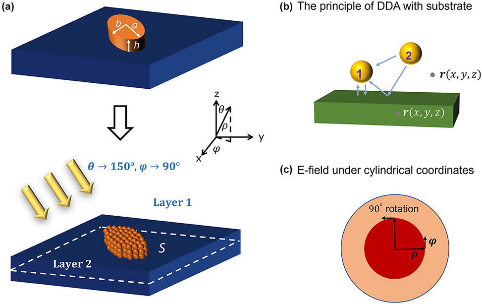
System geometry. (a) Structures on a substrate can be discretized into smaller, dipole-scale particles. To ensure our approach is generally applicable, symmetry is broken by choosing to simulate a rotated elliptic cylinder illuminated with an oblique plane wave. Two sizes of elliptic cylinder are simulated, as noted in the dimensions in panel (a). The incident wavelength is 1064 nm. The measurement plane is surface S, located 200 nm below the interface. (b) In the presence of a substrate, the DDA method is complicated by accounting for reflections off the substrate when computing interparticle coupling. (c) Diagram of the cylindrical coordinate system.
For the DDA approaches, the elliptic cylinder is discretized into individual dipoles with a pitch h/D, where D is a parameter we call the discretizing factor. The dipoles are uniformly distributed, so a larger D means more dipoles across all dimensions of the elliptic cylinder.
2.2 FDTD
FDTD is a popular nanophotonic simulation method due to its versatility and accuracy, which is a consequence of its ability to directly solve Maxwell’s equations. However, the time-iterated solver can be computationally inefficient for single-frequency simulations. In addition, the need for a gridded modeling region with cell size significantly smaller than the wavelength makes the simulation of large scale structures intractable. Furthermore, numerical artifacts can sometimes cause unstable and erroneous results. Errors can be minimized by choosing proper grid sizes and time steps. To ensure that our FDTD simulations serve as an accurate reference for testing our DDA approach, we used an underlying coarse grid with automatic nonuniform mesh accuracy setting of 2 for the outer regions of the simulation domain. We also applied a finer grid to the entire simulation region to avoid large numerical dispersion, and we tested different grid sizes (20 nm, 10 nm, 5 nm, and 3.5 nm), which approximately correspond to (λ/50, λ/100, λ/200, and λ/300). We found convergence for all materials at 3.5 nm grid size, with the worst case being for gold particles, where there was a 4 % difference in the maximum electric field along y-direction between the 3.5 nm and 5 nm grid sizes.
The auto-shut off values and time steps are set to 10−6 and 0.99, respectively, to assure convergence and accuracy.
2.3 Free-space DDA formulation
The scattering and absorption of electromagnetic waves by particles of arbitrary shape and composition can be simulated by the DDA method. Modeling this interaction in free space forms the basis for the model involving a substrate. When the wavelength is much larger than the particle size, the jth particle can be approximated as a single dipole with dipole moment,
where ɛ b is the background relative permittivity, E j is the electric field at dipole location r j , and α j is the polarizability of the dipole. For nonlinear processes, such as those in references [38, 39], higher order terms would also need to be included here. Polarizability can depend on particle shape, size, and material. There are various dipole models used for computing polarizabilities. In this paper, we will discuss four different dipole models based on Clausius–Mossotti relation, radiation reaction correction, digitized Green’s function, and lattice dispersion relation and how these polarizabilities affect the simulation results in Section 3.2. When not otherwise noted, we use the radiation reaction polarizability due to its high performance. The driving field for dipole j is the superposition of the incident field evaluated at r j and the scattered field from the other N − 1 particles with dipole moments p k at locations r k ,
where ω is the frequency of incident light, c denotes the speed of light, ɛ
0 is the vacuum permittivity, E
inc,j
is the incident field at the center of particle j, and
where r is the evaluation point, r
0
is the dipole location, R = r − r
0, R = |R|, k (when not used as a subscript) is the magnitude of the wave vector k,
which is a set of 3N linear equations for each of the components of the dipole moments p k . Once the dipole moments are known, the total electric field can be calculated at an arbitrary location r by,
A substrate can be incorporated into the free-space DDA formulation by discretizing the substrate into many dipoles. Here, we use a dipole spacing of 200 nm, distributed over an area of 9.8 μm × 9.8 μm and a depth of 1 μm. We compare the performance (speed and accuracy) of this computational approach to FDTD and the following two alternative DDA approaches. In the next formulation, reflections are calculated via two-dimensional Sommerfeld integrals in Cartesian coordinates, while in the final formulation, reflections are calculated via one-dimensional integrals in cylindrical coordinates.
2.4 Cartesian Green’s function: 2D integration
In this method, originally derived by W. Lukosz and R. E. Kunz in 1977 [30, 40], the light reflected by and/or transmitted through the substrate from a dipole source is analytically calculated, and these contributions are included as additional 2D Green’s functions, depicted by the blue arrows in Figure 1(b). Analogously to Equation (5), provided that the dipole moments are known, the electric field at an arbitrary location r can be calculated by [40],
where z > 0 corresponds to the background area (incident medium), and z < 0 corresponds to the substrate, as indicated in Figure 1, E
inc-ref and E
inc-tra are the reflected and transmitted incident fields calculated based on the Fresnel coefficients and Snell’s law (see Appendix A),
This calculation of the reflected Green’s function involves an integral over the angular spectrum of the field, as well as separate terms for s and p polarizations. The z-component of the wavevector is dependent upon the other two components according to,
The DDA problem analogous to Equation (4) becomes,
Although relatively straightforward, this 2D Green’s function approach has seen little application, principally because the Sommerfeld integrals in Equation (7) are difficult to evaluate numerically due to the infinite range of integration, high-frequency oscillatory behavior for large k
x
and k
y
, and an infinite number of singular points in
The reflection and transmission dyadics
2.5 Cylindrical Green’s function: 1D integration
We derive the cylindrical Green’s functions for a dipole above a substrate by starting from the cylindrical coordinate (ρ, φ, z) expressions for the electric field scattered by a single dipole located at
where R is the distance between the dipole and observation point, as in Equation (3). Note that the φ and dipole moment dependence can be easily separated out of these expressions with
A y-polarized dipole would have a scattered field that is a 90° counterclockwise rotation of the x-polarized dipole, as illustrated in Figure 1(c):
Since the polarization components are expressed in cylindrical coordinates in the above equation, no rotation in polarization is necessary in mapping the field from an x-polarized horizontal dipole to that of a y-polarized dipole. The electric field polarization components expressed in cylindrical coordinates can be converted to Cartesian components via multiplication with the rotation matrix,
Derived from the full expressions for the electric fields (Equations (9) and (10) and Appendix C), the scattered fields from x, y, and z-oriented dipoles can be concisely expressed using Green’s functions:
Equation (13) can be considered a definition for

Computational advantage of the 1D Green’s function over the 2D Green’s function. (a) Following the 2D Green’s function approach, the field over an area would have to be calculated at each pixel location. (b) Following the 1D approach, the slow computational step of Sommerfeld integral calculation, e.g., Equation (7), need only be calculated over one radial line and then mapped (interpolated) across the whole area by rapid multiplications with trigonometric functions of φ.
In the incident layer, these Green’s functions can be partitioned into a free-space part and a reflected part corresponding to the nonintegral and integral terms in the electric field expressions (e.g., Equations (9) and (10)):
The DDA problem analogous to Equations (4) and (8) is then:
Once the N dipole moments are found by solving the DDA problem, the scattered field at an arbitrary position r can be computed with Equation (6) using the 1D cylindrical Green’s functions in place of
The advantage of this 1D method is that it is very computationally efficient; the disadvantage is the instability of integration in the Green’s functions. Sommerfeld integrals with singular points are still involved and oscillation challenges still exist. Some of these singularities, e.g., at ρ = 0 are analytically removable using L’Hôpital’s rule (Appendix C). Two other singularities occur when the terms in the denominator of Equation (C3) equal zero: k
1z
= 0, k
2z
= 0 (Appendix C), which are k
ρ
= k
1, k
ρ
= k
2. We use the Gauss–Kronrod (GK) quadrature routine [40] to handle these singularities and evaluate
We use the built-in Matlab function quadgk to perform the GK routine. Several parameters must be considered for accurate and efficient computation: absolute and relative error, maximum number of subintervals, and the numerical truncation of k
ρ
at k
max instead of the analytical integration to infinity. Figure 3(a) shows how

Convergence of numerical computation of the infinite 1D Green’s function integrals. Unless otherwise noted, the parameters for each panel are ρ = 2 μm, z = z 0 = 1.8750 nm, ɛ b = 1, λ = 1064 nm, and ɛ sub = 3.55482 = 12.6366. (a) Azimuthal component of a scaled electric field above the substrate resulting from a horizontally polarized dipole as a function of different integral truncation values k max for two different sets of error tolerances. Loose tolerances correspond a relative tolerance of 10−3 and an absolute tolerance of 10−3 V/C, specified as options in quadgk. Tight tolerances correspond to a relative tolerance of 10−7 and an absolute tolerance of 10−7 V/C. (b) Scaled electric field as a function of the maximum number of subintervals used in quadgk for interval (k 2, k max). The brown line corresponds to the default parameters, while the black line corresponds to ɛ sub = 1.44962 = 2.1013, z = z 0 = 30 nm. (c) Convergence in electric field calculation for different dipole spacings and substrate materials. The orange line corresponds to the default parameters, while the blue line corresponds to ɛ sub = 1.44962 = 2.1013, z = z 0 = 30 nm. (d) Condition number of matrix A for gold elliptic nanocylinders with different choices of k max and different dipole spacings and substrate materials. The blue line corresponds to the system geometry illustrated in Section 2.1 with a = 300 nm, b = 90 nm, and h = 60 nm on a silica substrate with discretizing factor D = 3. The red line corresponds to a = 75 nm, b = 22.5 nm, and h = 15 nm on a silicon substrate with discretizing factor D = 3.
Based on the results of Figure 3 panels (a) and (b), we fix the relative tolerance at 10−7 and absolute tolerance at 10−7 V/C and maximum number of subintervals at 6000 and investigate the convergence properties for different dipole locations and substrate materials (Figure 3(c)). Convergence is generally slower for smaller dipole spacings and higher substrate refractive indices. To further ensure all values in the coupling matrix
Now, we can accurately and efficiently calculate
Because the Green’s functions
3 Results and discussion
3.1 Computational time
For metasurface design applications, both accuracy and computational time are important. With unlimited computational resources, the methods in Sections 2.2, 2.3, 2.4, and 2.5 would produce the same results. In reality, the performance varies significantly.
To compute the electromagnetic field scattered by a nanostructure, the DDA codes require time to execute several key steps: t 1 to compute the incident field at all dipoles, t 2 to build up the 3N × 3N Green’s function coupling matrix, t 3 to solve the matrix problem for the unknown dipole moments, and t 4 to compute the scattered field from all dipoles. We denote the individual computational times related to these steps as s 1 to compute the incident field at a single dipole location, s 2 to compute a single term in the coupling matrix by parallel computing, s 3 to solve for all of the unknown dipole moments, and s 4 to compute the field scattered by a single dipole over a monitor sampling area q x × q y = 102 × 108 points by parallel computing. Note that t 3 = s 3 as solving for the dipole moments is a single step.
To compare the computational times, we use the system geometry illustrated in Section 2.1 with a gold elliptic cylinder (a = 300 nm, b = 90 nm, h = 60 nm) on a silica substrate with discretizing factor D = 2 over a monitor size of 2 μm × 2 μm. For the 2D Cartesian and 1D cylindrical Green’s function methods, there are N ns = 200 nanostructure dipoles in the system, and the monitor is located at z = −200 nm. For the substrate discretization method, there are an additional N sub = 12,005 substrate dipoles, and monitor is located at z = 200 nm to avoid computing the fields inside the substrate dipoles. The results are shown in Table 1.
Discrete dipole approximation computational times. Total time for each step (t) as well as individual element time (s) is provided. See the main text for the precise definitions of each of these steps. The simulation times correspond to specific single runs on our server, and thus our choice of reporting results to three significant figures is not intended to indicate any measure of uncertainty.
| Substrate discretization | 2D Green’s function | 1D Green’s function | |
|---|---|---|---|
| N | 12,205 | 200 | 200 |
| t 1[s] | 1.15 | 5.96 × 10⁻² | 5.86 × 10⁻² |
| t 2[s] | 389 | 1.69 × 10⁴ | 31.4 |
| t 3[s] | 377 | 1.91 × 10⁻² | 1.66 × 10⁻² |
| t 4[s] | 41.1 | 1.62 × 10⁴ | 22.2 |
| t total[s] | 807 | 3.32 × 10⁴ | 53.6 |
| s 1[s] | 9.43 × 10⁻⁵ | 2.98 × 10⁻⁴ | 2.93 × 10⁻⁴ |
| s 2[s] | 8.70 × 10⁻⁷ | 2.34 × 10⁻² | 3.12 × 10⁻⁴ |
| s 3[s] | 377 | 1.92 × 10⁻² | 1.66 × 10⁻² |
| s 4[s] | 3.37 × 10⁻³ | 81.1 | 0.111 |
| Pattern error [%] | 44.7 | 4.58 | 4.21 |
| Power error [%] | 3.04 × 10³ | 22.4 | 28.7 |
These simulations are executed on our lab’s server with specs: dual Intel Xeon CPU E5-2660 v3 @2.6 GHz processors, each with 10 real cores and 10 virtual cores that combine to provide 40 logical processors altogether, and 256 GB of 2133 MT/s RDIMM memory. We are able to use the parallel computing toolbox of Matlab to compute steps 2 and 4 described above because the 3 × 3 Green’s functions are independent of each other, as are the scattered fields from different dipoles with known dipole moments. Matlab is able to use 20 workers on our server, which is equivalent to ∼50 % CPU.
For all of our computational approaches, the time required to calculate the incident field at all dipole locations is small compared to the total time and, therefore, t
1 can be neglected. The symmetry and antisymmetry between
For the substrate discretization method, the substrate is typically very large compared to the nanostructure, effectively extending to infinity. Therefore, a large N
sub is required for accurate results with minimal diffraction artifacts from truncation. We find that balancing the demand for computational resources against desired accuracy typically results in N
sub > 105, while the nanostructure itself only requires N
ns ∼ 103 or fewer due to its small, wavelength-scale size. So the number of substrate dipoles dominates the computational time. Furthermore, the calculation of the field at the monitor location is computationally similar to the calculation of the individual elements of the coupling matrix, so s
4,sd ≈ 6s
2,sd q
x
q
y
, where the factor of 6 is the number of independent terms in the Green’s function. Combining all steps and applying symmetry and antisymmetry between
For the 2D Cartesian Green’s function method, there are no substrate dipoles because substrate reflections are incorporated into the Green’s function itself, N = N ns. Again, s 4,2D ≈ 6s 2,2D q x q y . The computational time is
Compared to the substrate discretization method, the biggest advantage is that N is several orders of magnitude smaller. However, the value of s 2 increases significantly because of the 2D Green’s function Sommerfeld integrals involved in Equation(7). On the other hand, s 3 is significantly reduced compared to the substrate discretization method due to the smaller N.
For the 1D cylindrical Green’s function method, the computational time is similarly,
3.2 Dipole modeling effects on the DDA-with-substrate methods
We compare the real and imaginary parts of the electric field over surface S (see Figure 1) computed by our 1D Green’s function method to those from our gold standard FDTD simulations, as shown in Figure 4. Out of all the DDA methods, we concentrate on the 1D cylindrical Green’s function method, because it possesses the best computational performance as discussed above. The electric fields computed by the two methods are almost identical for all six electric field components. Considering that Matlab is only able to use physical cores and not virtual cores, only up to 50 % of server processors are utilized. For a fair comparison, we manually change the resource settings in Lumerical to ensure that the same number of processors are used in multithreading. The FDTD simulations take 1823 s, while the 1D Green’s function method only takes 293 s to converge.
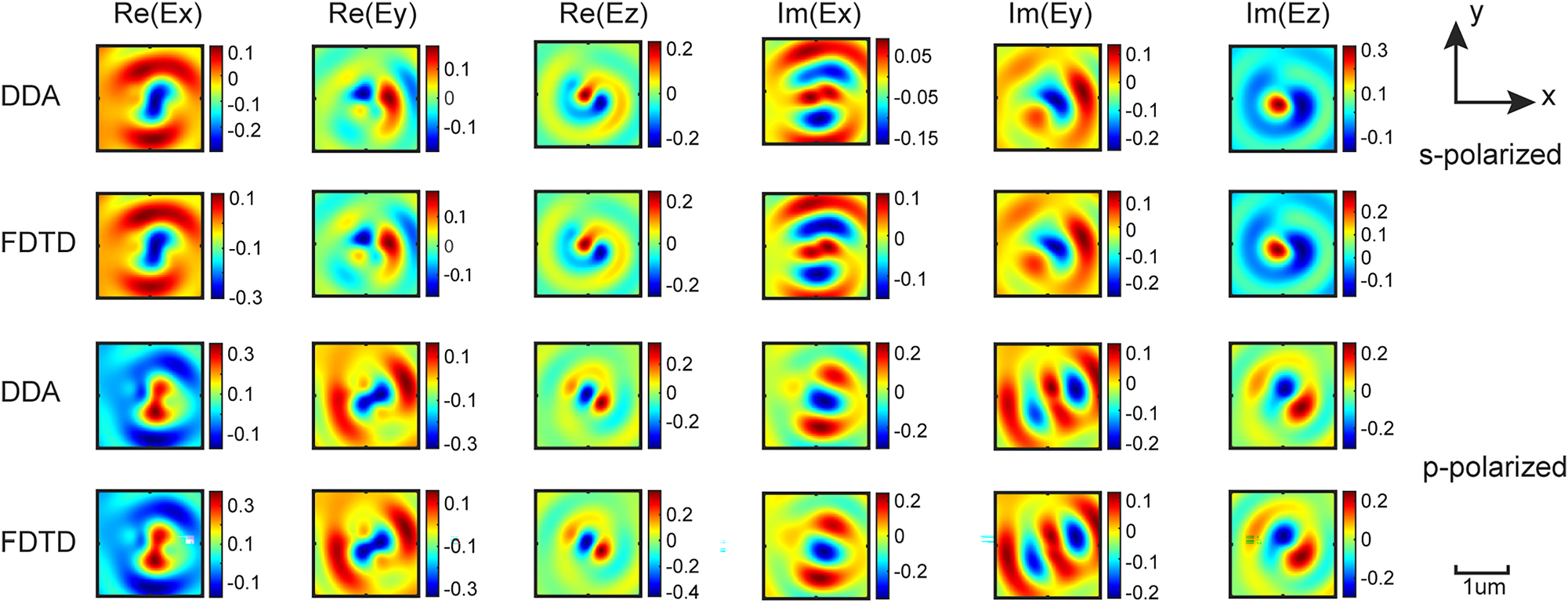
Converged 1D cylindrical Green’s function DDA results validated against FDTD. The real and imaginary parts of electric field computed by the 1D cylindrical Green’s function DDA and FDTD methods for the larger gold elliptic cylinder (a = 300 nm, b = 90 nm, h = 60 nm) at a discretizing factor D = 3.
To quantitatively compare the field difference between our 1D Green’s function method and the FDTD method, we introduce two parameters called pattern error and power error:
The pattern error pertains to the calculation of correlation coefficients between the real and imaginary components of the x, y, and z components of the electric field over surface S between the 1D cylindrical Green’s function and FDTD methods. A correlation coefficient of 1 indicates a perfect match between these two methods, discounting any potential total power discrepancy, while 0 signifies no match at all. The pattern error quantifies the average deviation of each component from a 100 % similarity between these two methods. The power error captures the average power percentage differences of the electric field. Significantly, the pattern error holds greater importance as it is predominantly shaped by two key factors: the relative Green’s function values across S and the relative dipole moments of all particles. Conversely, the power error is primarily attributed to variations in polarizabilities computed from different dipole models, and its mitigation hinges on the pursuit of more precise dipole models. Furthermore, total power errors could be corrected by a simple constant multiplicative correction factor, whereas pattern errors cannot be simply corrected.
A prerequisite of accurate DDA simulations is a precise dipole model. Point dipoles, by definition, have infinitesimal volumes and, therefore, are theoretically approximated models. As mentioned in Section 2.3, small particles can be approximated as dipoles, and their dipole moments can by computed by Equation (1). The most common dipole model used to compute the polarizabilities α is the Clausius–Mossotti (CM) relation [43]:
where ɛ is the complex permittivity of the particle, V = d 3 is the volume of cubic voxels, and d is the dipole spacing. The reason that we use cubic voxels is so that the discretized dipoles are close-packed and occupy the full volume of the nanostructure. For improved accuracy for larger d, one can account for the back-action of the scattered field on the dipole using the radiation reaction correction (RR) [44]:
The digitized Green’s function (DGF) dipole model includes corrections on the order of
To accurately reproduce wave propagation and the dispersion relation in an infinite medium, the lattice dispersion relation (LDR) dipole model was proposed by Draine and Goodman [46] as:
where
We evaluated these four dipole models using the large gold elliptical cylinder (a = 300 nm, b = 90 nm, h = 60 nm) on a silica substrate with D = 3. The pattern and power errors shown in Figure 5 are calculated over a 2 μm × 2 μm monitor located at z = −200 nm. FDTD simulation results again serve as our gold-standard. Among these four dipole models, the CM and RR models provided less than 1 % pattern error for both polarizations. However, the power errors are slightly larger, ranging from 5 % to 15 %. We consider pattern errors as a more fundamental error, since power errors can be corrected by simply multiplying a constant factor. The DGF dipole model gives the best balance between pattern and power error, with pattern errors around 3 % for both polarizations, and power errors around 7 %. The cubical subvolume dipole assumption makes the DGF model have the best power errors among all four dipole models. The LDR dipole model gives the worst performance for both pattern and power errors, and therefore we do not recommend it for metasurface simulations.

Effect of different dipole models. (a) Effect on pattern error. (b) Effect on power error.
3.3 Materials and shape effects on the DDA-with-substrate methods
We proceeded to assess the impact of different materials on the performance of the DDA-with-substrate methods. Figure 6 panel (a) shows how pattern errors change as a function of discretizing factor D. We tested two different particle materials: gold and germanium under both s- and p-polarization because metallic and high-index dielectric blocks are widely applied in metasurface applications. In all cases, the pattern errors reduce rapidly and reach our chosen convergence criteria: pattern error

Comparison between the 1D cylindrical Green’s function method and the FDTD method. A large elliptic cylinder (a = 300 nm, b = 90 nm, h = 60) is simulated. (a)–(c) Results for different nanoparticle materials on a silica substrate illuminated with different polarizations. (d)–(f) Results for a gold nanoparticle on different substrate materials, illuminated with different polarizations.
Some integrated optics applications that require CMOS-compatible fabrication techniques and reflective metasurfaces typically use silicon as the substrate, so we also investigate how the substrate refractive index affects the simulation accuracy. We examine gold nanoparticles, keeping the other parameters the same. Figure 6 panels (d) and (e) compare the silicon and silica substrate. The pattern errors and power errors are significantly greater for the silicon substrate under both polarizations. Even at large discretizing factor D = 4, the pattern errors and power errors are approximately 20 % and 45 %, respectively.
Our server memory limits our ability to test cases with D > 4. So in order to test smaller dipole spacings, we shrink the dimensions of the elliptic cylinder to a = 75 nm, b = 22.5 nm, and h = 15 nm, which makes it quarter-scale compared to the original elliptic cylinder. Considering the definition of discretizing factor, D = 1, 2, 3, and 4 for small elliptic cylinders corresponds to the same dipole spacing as D = 4, 8, 12, and 16 in large elliptic nanocylinders. The recorded electric field over surface S in Figure 7 with a silicon substrate shows excellent pattern agreement and acceptable power agreement between the 1D Green’s function and the FDTD method. Panels (b) and (c) in Figure 7 show that the pattern errors and power errors change as a function of discretizing factor. Compared with the large elliptic cylinder, the pattern and power error reduce significantly for both polarizations. For pattern errors, they reach our convergence criteria when D = 2, and for power errors, we believe that they may be further reduced by using smaller dipole spacing. In actual applications, the power error is less important than the pattern error, as we can scale the electromagetic fields by multiplying a constant to correct power errors, rather than using smaller dipole spacing. Panel (d) of Figure 7 shows similar computational time and scaling as for the large elliptic cylinder in Figure 6.
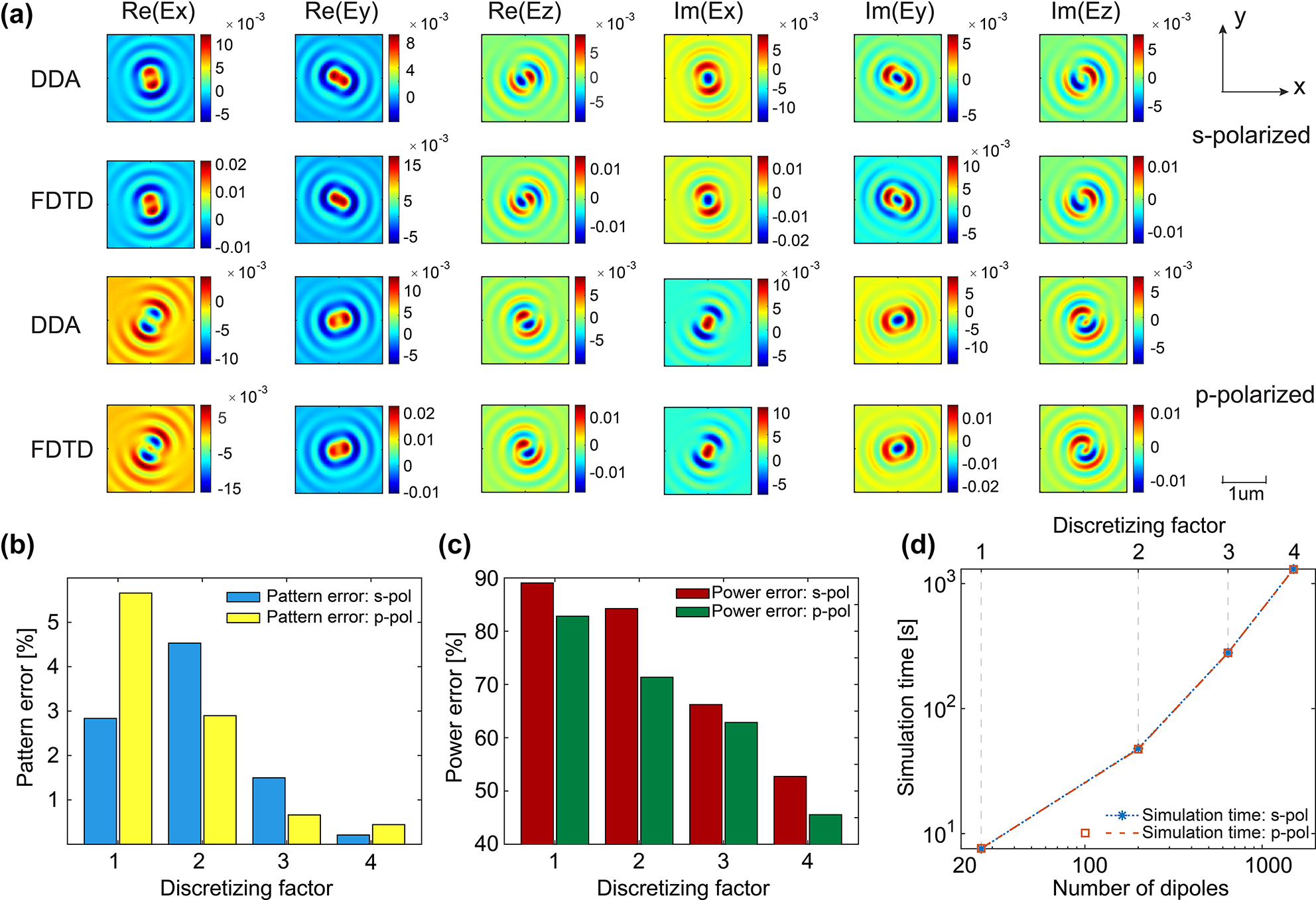
DDA-with-substrate simulation results for the smaller gold elliptic cylinder (a = 75 nm, b = 22.5 nm, h = 15 nm). (a) The real and imaginary parts of electric field computed by the 1D cylindrical Green’s function DDA-with-substrate method validated against FDTD calculations for the high refractive index substrate (silicon) with a discretizing factor D = 3. The patterns between the two methods are similar, while the power differences are greater. (b) Pattern error between the DDA and FDTD simulations. (c) Power error between the two simulations. (d) Computational time scaling of the DDA simulations.
We also investigated the impact of nanostructure shape dimensions on pattern and power errors by conducting two more tests on elliptical cylinders as depicted in Figure 1(a). The dimensions of these structures and results are presented in Table 2. For a fair comparison, we selected the same source wavelength and incidence angle as before, as well as the same monitor surface S. In this comparison, the elliptical cylinders are composed of germanium, and the substrates are silica. One of the elliptical cylinders is taller, with only a few dipoles touching the substrate, while the other is flatter, with many dipoles in contact with the substrate. Across all three elliptical cylinders with different dimensions, the pattern error remains largely consistent, whereas the power error increases as more dipoles come into contact with the substrate. At present, determining a correction factor for the overall power requires corresponding FDTD simulations.
Accuracy of the 1D cylindrical Green’s function for elliptical cylinders of different dimensions. The pattern error is consistently low, while the power error increases when more dipoles are in close proximity to the substrate. In all cases, the dipole pitch is 20 nm.
| Standard elliptical cylinder | Flatter elliptical cylinder | Taller elliptical cylinder | |
|---|---|---|---|
| Dimensions (a, b, h) [nm] | (300,90,60) | (200,100,40) | (50,50,100) |
| Short axis angle | ϕ = 150° | ϕ = 45° | ϕ = 0° |
| N | 642 | 320 | 105 |
| Pattern error [%] | 2.66 | 1.08 | 0.064 |
| Power error [%] | 13.80 | 47.37 | 14.75 |
The above simulations and comparisons illustrate the main advantage of the 1D cylindrical Green’s function over techniques such as FDTD: the computational time scales with number of particles and monitor sampling points rather than domain size. This allows for monitors of arbitrary size and far field calculations without requiring a projection from the near field. As a result, this method can be used for many applications that cannot be simulated by FDTD, such as weak coupling of distant small particles and accurate scattering patterns over large simulation regions (e.g., in wafer inspection). Another advantage of the DDA approach over “black-box” machine learning techniques is that the dipole moment distribution throughout the structure can be used to provide physical understanding of what parts structure contribute the most to its optical properties.
There are a few limitations of our 1D cylindrical Green’s function method. Firstly, it is difficult to deal with nonlinear optical properties, specifically second harmonic generation from nanoparticles [38] or four-wave mixing in metasurfaces [39]. Equation (1) assumes a linear relationship between the polarization and local (driving) field. For nonlinear optical properties, higher order local fields like E j ⊗E j need to be incorporated into the dipole moment. Secondly, our approach currently models a domain in isolation, rather than a periodic array. However, thousands of dipoles can be simulated, and these dipoles need not be in the same metasurface particle, so modest arrays of elements could be simulated. Infinite periodic arrays can be simulated using a generalized DDA formulation, as outlined in Draine and Flatau’s 2008 work [47] or by applying the Bloch theorem to compute the effective polarizability of nanoparticles in a lattice, as discussed in the paper [48]. Furthermore, reference [48] provides analytical expressions for using the DDA method to compute the scattering matrix between layers in rigorous coupled-wave analysis (RCWA). However, it encounters challenges related to low convergence and accuracy near an interface. Our 1D cylindrical Green’s function method may serve as a valuable tool to address these challenges in the future.
4 Conclusions
We tested our DDA-with-substrate method for metallic and dielectric particle materials, both low and high refractive index substrate materials, different sizes of structures, and different polarization states of incident light. Our results are for a wavelength of 1064 nm, and while there is nothing special about this wavelength, extrapolation to other wavelengths would need to be verified. The DDA-with-substrate method using a 1D cylindrical Green’s function is a general, efficient, and accurate method for the scattered field calculation from structures on substrate and can be widely used in metasurface design applications. Easier systems, such as dielectric particles with low indices, can also be simulated with low error. Note that although the Green’s function approach generalizes to any kind of monitor, our 1D cylindrical Green’s function method is particularly efficient for monitor planes perpendicular to the z-axis (see discussion preceding Equation (18)). Compared with the FDTD method, the computational time of our DDA method is at least one order of magnitude faster with the same level of accuracy for the low refractive index substrate. For high refractive index substrates like silicon, our method achieves a 98 % similarity in the electric field pattern, however, with a relatively large power error that may be mitigated by applying a correction factor. All the codes are written in Matlab, and the metasurface design process can be implemented without purchasing FDTD or FEM software.
Funding source: National Science Foundation
Award Identifier / Grant number: ECCS-1807590
Award Identifier / Grant number: ECCS-2045220
-
Research funding: This research was supported in part by the National Science Foundation’s (http://dx.doi.org/10.13039/100000001) grants ECCS-1807590 and ECCS-2045220.
-
Author contributions: All authors have accepted responsibility for the entire content of this manuscript and approved its submission.
-
Conflict of interest: Drs. McLeod and Liu are inventors on intellectual property related to nanophotonic design approaches.
-
Data availability: All data related to this manuscript will be made available by the authors upon reasonable request.
Appendix A: Cartesian Green’s function
The equations in this appendix follow the derivation from reference [40]. The analytical solutions of a dipole near layered substrate can be expressed as 2D integrations in (k x , k y ) space (Equation (7)). The two parts of the integrand in Equation (7) are defined as,
The transmitted Green’s function in layer 2 of Figure 1 is:
Similarly,
The variables r s (k x , k y ), r p (k x , k y ), t s (k x , k y ), and t p (k x , k y ) in Equations (A1) and (A3) are the Fresnel coefficients and can be computed as:
With an assumption of dielectric substrate materials, the singular points in
Appendix B: trapz for 2D Sommerfeld integration
Accurate integration using trapz() requires varying k max and the number of sampling points in frequency space for different dipole heights z 0. The values used in this paper are listed in Table B1.
Parameters for calculating 2D Cartesian Green’s functions using the built-in Matlab function trapz.
| For dipole heights | Parameters for
|
For dipole heights | Parameters for
|
||
|---|---|---|---|---|---|
| z 0 in the range | k max | Sampling points | z 0 in the range | k max | Sampling points |
| (0, 20] nm | 250k 1 | 3104 × 3106 | (0, 10] nm | 180k 1 | 2104 × 2106 |
| (20, 100] nm | 80k 1 | 1204 × 1206 | (10, 100] nm | 60k 1 | 804 × 806 |
| (100, 250] nm | 30k 1 | 804 × 806 | (100, 250] nm | 30k 1 | 504 × 506 |
| (250, 500] nm | 10k 1 | 504 × 506 | (250, 500] nm | 10k 1 | 204 × 206 |
| (500, 1000] nm | 5k 1 | 204 × 206 | (500, 1000] nm | 5k 1 | 104 × 106 |
| (1000, ∞) nm | 3k 1 | 104 × 106 | (1000, ∞) nm | 3k 1 | 54 × 56 |
Appendix C: Cylindrical Green’s function
The equations in this appendix are adapted from reference [40] from a 3-layer system to a 2-layer system. The analytical solutions of a dipole a near layered substrate can be expressed as 1D integrations in k ρ space. The scattered fields in layer 1 of Figure 1, including those reflected off the substrate, are given by:
where the superscript H represents a horizontal dipole and the superscript V represents for the vertical dipole. See below Equation (10) in the main text for parameter definitions. The electric field in layer 2, which is illustrated in Figure 1, can be expressed as:
The A, B, and C coefficients in Equations (C1) and (C2) are given by:
where the f and g coefficients are related to the Fresnel coefficients, specifically:
Similar to the 2D Green’s function, the singular points in the 1D Green’s function occur when the denominators of Equations (C1) and (C2) equal zero, i.e., when ρ = 0, k
ρ
= k
1, or k
ρ
= k
2. The singular point ρ = 0 is independent of the integration variable k
ρ
and is removable by using L’Hôpital’s rule. Considering only the reflected part of Equation (C1), and substituting the values of Bessel functions J
0(0) = 1 and
Note that as ρ approaches 0, the directions of the cylindrical unit vectors depend on the chosen direction of approach. It is important to keep track of these directions when converting back to a Cartesian system.
References
[1] N. Yu and F. Capasso, “Flat optics with designer metasurfaces,” Nat. Mater., vol. 13, no. 2, pp. 139–150, 2014. https://doi.org/10.1038/nmat3839.Suche in Google Scholar PubMed
[2] R. Alaee, M. Albooyeh, and C. Rockstuhl, “Theory of metasurface based perfect absorbers,” J. Phys. D: Appl. Phys., vol. 50, no. 50, p. 503002, 2017. https://doi.org/10.1088/1361-6463/aa94a8.Suche in Google Scholar
[3] M. Y. Shalaginov, S. An, Y. Zhang, et al.., “Reconfigurable all-dielectric metalens with diffraction-limited performance,” Nat. Commun., vol. 12, no. 1, pp. 1–8, 2021. https://doi.org/10.1038/s41467-021-21440-9.Suche in Google Scholar PubMed PubMed Central
[4] D. Zhang, M. Ren, W. Wu, et al.., “Nanoscale beam splitters based on gradient metasurfaces,” Opt. Lett., vol. 43, no. 2, pp. 267–270, 2018. https://doi.org/10.1364/ol.43.000267.Suche in Google Scholar PubMed
[5] S. Wang, Z.-L. Deng, Y. Wang, et al.., “Arbitrary polarization conversion dichroism metasurfaces for all-in-one full poincaré sphere polarizers,” Light: Sci. Appl., vol. 10, no. 1, pp. 1–9, 2021. https://doi.org/10.1038/s41377-021-00468-y.Suche in Google Scholar PubMed PubMed Central
[6] S. Jafar-Zanjani, S. Inampudi, and H. Mosallaei, “Adaptive genetic algorithm for optical metasurfaces design,” Sci. Rep., vol. 8, no. 1, pp. 1–16, 2018. https://doi.org/10.1038/s41598-018-29275-z.Suche in Google Scholar PubMed PubMed Central
[7] H. Chung and O. D. Miller, “Tunable metasurface inverse design for 80% switching efficiencies and 144 angular deflection,” ACS Photonics, vol. 7, no. 8, pp. 2236–2243, 2020.10.1021/acsphotonics.0c00787Suche in Google Scholar
[8] T. Qiu, X. Shi, J. Wang, et al.., “Deep learning: a rapid and efficient route to automatic metasurface design,” Advanced Science, vol. 6, no. 12, p. 1 900 128, 2019. https://doi.org/10.1002/advs.201900128.Suche in Google Scholar PubMed PubMed Central
[9] I. Tanriover, W. Hadibrata, and K. Aydin, “Physics-based approach for a neural networks enabled design of all-dielectric metasurfaces,” ACS Photonics, vol. 7, no. 8, pp. 1957–1964, 2020. https://doi.org/10.1021/acsphotonics.0c00663.Suche in Google Scholar
[10] D. Melati, Y. Grinberg, M. Kamandar Dezfouli, et al.., “Mapping the global design space of nanophotonic components using machine learning pattern recognition,” Nat. Commun., vol. 10, no. 1, pp. 1–9, 2019. https://doi.org/10.1038/s41467-019-12698-1.Suche in Google Scholar PubMed PubMed Central
[11] Y. Kiarashinejad, S. Abdollahramezani, and A. Adibi, “Deep learning approach based on dimensionality reduction for designing electromagnetic nanostructures,” npj Comput. Mater., vol. 6, no. 1, pp. 1–12, 2020. https://doi.org/10.1038/s41524-020-0276-y.Suche in Google Scholar
[12] K. Yee, “Numerical solution of initial boundary value problems involving Maxwell’s equations in isotropic media,” IEEE Trans. Antennas Propag., vol. 14, no. 3, pp. 302–307, 1966. https://doi.org/10.1109/TAP.1966.1138693.Suche in Google Scholar
[13] C.-H. Poh, L. Rosa, S. Juodkazis, and P. Dastoor, “Fdtd modeling to enhance the performance of an organic solar cell embedded with gold nanoparticles,” Opt. Mater. Express, vol. 1, no. 7, pp. 1326–1331, 2011. https://doi.org/10.1364/ome.1.001326.Suche in Google Scholar
[14] A. K. Goyal and S. Pal, “Design and simulation of high sensitive photonic crystal waveguide sensor,” Optik, vol. 126, no. 2, pp. 240–243, 2015. https://doi.org/10.1016/j.ijleo.2014.08.174.Suche in Google Scholar
[15] V. Donzella, A. Sherwali, J. Flueckiger, S. M. Grist, S. T. Fard, and L. Chrostowski, “Design and fabrication of soi micro-ring resonators based on sub-wavelength grating waveguides,” Opt. Express, vol. 23, no. 4, pp. 4791–4803, 2015. https://doi.org/10.1364/oe.23.004791.Suche in Google Scholar
[16] B. T. Draine and P. J. Flatau, “Discrete-dipole approximation for scattering calculations,” JOSA A, vol. 11, no. 4, pp. 1491–1499, 1994. https://doi.org/10.1364/josaa.11.001491.Suche in Google Scholar
[17] L. Ling, F. Zhou, L. Huang, and Z.-Y. Li, “Optical forces on arbitrary shaped particles in optical tweezers,” J. Appl. Phys., vol. 108, no. 7, p. 073 110, 2010. https://doi.org/10.1063/1.3484045.Suche in Google Scholar
[18] H. Okamoto and Y.-L. Xu, “Light scattering by irregular interplanetary dust particles,” Earth, Planets Space, vol. 50, no. 6, pp. 577–585, 1998. https://doi.org/10.1186/bf03352151.Suche in Google Scholar
[19] M. Kocifaj and G. Videen, “Optical behavior of composite carbonaceous aerosols: dda and emt approaches,” J. Quant. Spectrosc. Radiat. Transfer, vol. 109, no. 8, pp. 1404–1416, 2008. https://doi.org/10.1016/j.jqsrt.2007.11.007.Suche in Google Scholar
[20] W.-H. Yang, G. C. Schatz, and R. P. Van Duyne, “Discrete dipole approximation for calculating extinction and Raman intensities for small particles with arbitrary shapes,” J. Chem. Phys., vol. 103, no. 3, pp. 869–875, 1995. https://doi.org/10.1063/1.469787.Suche in Google Scholar
[21] M. A. Taubenblatt and T. K. Tran, “Calculation of light scattering from particles and structures on a surface by the coupled-dipole method,” JOSA A, vol. 10, no. 5, pp. 912–919, 1993. https://doi.org/10.1364/josaa.10.000912.Suche in Google Scholar
[22] R. Schmehl, B. M. Nebeker, and E. D. Hirleman, “Discrete-dipole approximation for scattering by features on surfaces by means of a two-dimensional fast fourier transform technique,” JOSA A, vol. 14, no. 11, pp. 3026–3036, 1997. https://doi.org/10.1364/josaa.14.003026.Suche in Google Scholar
[23] M. A. Yurkin and M. Huntemann, “Rigorous and fast discrete dipole approximation for particles near a plane interface,” J. Phys. Chem. C, vol. 119, no. 52, pp. 29088–29094, 2015. https://doi.org/10.1021/acs.jpcc.5b09271.Suche in Google Scholar
[24] D. F. Carvalho, M. A. Martins, P. A. Fernandes, and M. R. P. Correia, “Coupling of plasmonic nanoparticles on a semiconductor substrate via a modified discrete dipole approximation method,” Phys. Chem. Chem. Phys., vol. 24, no. 33, pp. 19 705–719 715, 2022. https://doi.org/10.1039/d2cp02446b.Suche in Google Scholar PubMed
[25] A. E. Miroshnichenko, A. B. Evlyukhin, Y. S. Kivshar, and B. N. Chichkov, “Substrate-induced resonant magnetoelectric effects for dielectric nanoparticles,” ACS Photonics, vol. 2, no. 10, pp. 1423–1428, 2015. https://doi.org/10.1021/acsphotonics.5b00117.Suche in Google Scholar
[26] M. M. Salary, A. Forouzmand, and H. Mosallaei, “Model order reduction of large-scale metasurfaces using a hierarchical dipole approximation,” ACS Photonics, vol. 4, pp. 63–75, 2017. https://doi.org/10.1021/acsphotonics.6b00568.Suche in Google Scholar
[27] V. L. Loke and M. P. Mengüç, “Surface waves and atomic force microscope probe-particle near-field coupling: discrete dipole approximation with surface interaction,” JOSA A, vol. 27, no. 10, pp. 2293–2303, 2010. https://doi.org/10.1364/josaa.27.002293.Suche in Google Scholar PubMed
[28] V. L. Loke, M. P. Mengüç, and T. A. Nieminen, “Discrete-dipole approximation with surface interaction: computational toolbox for matlab,” J. Quant. Spectrosc. Radiat. Transfer, vol. 112, no. 11, pp. 1711–1725, 2011. https://doi.org/10.1016/j.jqsrt.2011.03.012.Suche in Google Scholar
[29] M. R. Short, J.-M. Geffrin, R. Vaillon, H. Tortel, B. Lacroix, and M. Francoeur, “Evanescent wave scattering by particles on a surface: validation of the discrete dipole approximation with surface interaction against microwave analog experiments,” J. Quant. Spectrosc. Radiat. Transfer, vol. 146, pp. 452–458, 2014. https://doi.org/10.1016/j.jqsrt.2013.12.007.Suche in Google Scholar
[30] W. Lukosz and R. E. Kunz, “Light emission by magnetic and electric dipoles close to a plane interface I Total radiated power,” J. Opt. Soc. Am., vol. 67, no. 12, p. 1607, 1977. https://doi.org/10.1364/josa.67.001607.Suche in Google Scholar
[31] M. A. Yurkin and A. G. Hoekstra, “The discrete-dipole-approximation code adda: capabilities and known limitations,” J. Quant. Spectrosc. Radiat. Transfer, vol. 112, no. 13, pp. 2234–2247, 2011. https://doi.org/10.1016/j.jqsrt.2011.01.031.Suche in Google Scholar
[32] M. Shabaninezhad, M. Awan, and G. Ramakrishna, “Matlab package for discrete dipole approximation by graphics processing unit: fast fourier transform and biconjugate gradient,” J. Quant. Spectrosc. Radiat. Transfer, vol. 262, p. 107 501, 2021. https://doi.org/10.1016/j.jqsrt.2020.107501.Suche in Google Scholar
[33] P. C. Chaumet, “The discrete dipole approximation: a review,” Mathematics, vol. 10, no. 17, p. 3049, 2022. https://doi.org/10.3390/math10173049.Suche in Google Scholar
[34] S. Babar and J. H. Weaver, “Optical constants of Cu, Ag, and Au revisited,” Appl. Opt., vol. 54, no. 3, pp. 477–481, 2015. https://doi.org/10.1364/ao.54.000477.Suche in Google Scholar
[35] T. N. Nunley, N. S. Fernando, N. Samarasingha, et al.., “Optical constants of germanium and thermally grown germanium dioxide from 0.5 to 6.6eV via a multisample ellipsometry investigation,” J. Vac. Sci. Technol., B, vol. 34, no. 6, p. 061 205, 2016. https://doi.org/10.1116/1.4963075.Suche in Google Scholar
[36] I. H. Malitson, “Interspecimen comparison of the refractive index of fused silica*,†,” JOSA, vol. 55, no. 10, pp. 1205–1209, 1965. https://doi.org/10.1364/JOSA.55.001205.Suche in Google Scholar
[37] C. Schinke, P. Christian Peest, J. Schmidt, et al.., “Uncertainty analysis for the coefficient of band-to-band absorption of crystalline silicon,” AIP Adv., vol. 5, no. 6, p. 067 168, 2015. https://doi.org/10.1063/1.4923379.Suche in Google Scholar
[38] N. K. Balla, P. T. So, and C. J. Sheppard, “Second harmonic scattering from small particles using discrete dipole approximation,” Opt. Express, vol. 18, no. 21, pp. 21 603–621 611, 2010. https://doi.org/10.1364/oe.18.021603.Suche in Google Scholar
[39] D. Shen, J. Cao, and W. Wan, “Wavefront shaping with nonlinear four-wave mixing,” Sci. Rep., vol. 13, no. 1, p. 2750, 2023. https://doi.org/10.1038/s41598-023-29621-w.Suche in Google Scholar PubMed PubMed Central
[40] L. Novotny and B. Hecht, Principles of Nano-Optics, Cambridge, UK, Cambridge University Press, 2012.10.1017/CBO9780511794193Suche in Google Scholar
[41] T. Cui and W. Chew, “Efficient evaluation of Sommerfeld integrals for TM wave scattering by buried objects,” J. Electromagn. Waves Appl., vol. 12, no. 5, pp. 607–657, 1998. https://doi.org/10.1163/156939398x00160.Suche in Google Scholar
[42] L. Novotny, “Allowed and forbidden light in near-field optics. i. a single dipolar light source,” JOSA A, vol. 14, no. 1, pp. 91–104, 1997. https://doi.org/10.1364/josaa.14.000091.Suche in Google Scholar
[43] P. V. Rysselberghe, “Remarks concerning the Clausius-Mossotti law,” J. Phys. Chem., vol. 36, no. 4, pp. 1152–1155, 2002. https://doi.org/10.1021/j150334a007.Suche in Google Scholar
[44] B. T. Draine, “The discrete-dipole approximation and its application to interstellar graphite grains,” Astrophys. J., Part 1, vol. 333, pp. 848–872, 1988. https://doi.org/10.1086/166795.Suche in Google Scholar
[45] G. H. Goedecke and S. G. O’Brien, “Scattering by irregular inhomogeneous particles via the digitized green’s function algorithm,” Appl. Opt., vol. 27, no. 12, pp. 2431–2438, 1988. https://doi.org/10.1364/ao.27.002431.Suche in Google Scholar
[46] B. T. Draine and J. Goodman, “Beyond Clausius-Mossotti-wave propagation on a polarizable point lattice and the discrete dipole approximation,” Astrophys. J., Part 1, vol. 405, no. 2, pp. 685–697, 1993. https://doi.org/10.1086/172396.Suche in Google Scholar
[47] B. T. Draine and P. J. Flatau, “Discrete-dipole approximation for periodic targets: theory and tests,” JOSA A, vol. 25, no. 11, pp. 2693–2703, 2008. https://doi.org/10.1364/josaa.25.002693.Suche in Google Scholar PubMed
[48] I. M. Fradkin, S. A. Dyakov, and N. A. Gippius, “Fourier modal method for the description of nanoparticle lattices in the dipole approximation,” Phys. Rev. B, vol. 99, no. 7, p. 075 310, 2019. https://doi.org/10.1103/physrevb.99.075310.Suche in Google Scholar
© 2023 the author(s), published by De Gruyter, Berlin/Boston
This work is licensed under the Creative Commons Attribution 4.0 International License.
Artikel in diesem Heft
- Frontmatter
- Research Articles
- Reconfigurable polarization processor based on coherent four-port micro-ring resonator
- Multiplexing in photonics as a resource for optical ternary content-addressable memory functionality
- Fast and accurate electromagnetic field calculation for substrate-supported metasurfaces using the discrete dipole approximation
- Robust reconfigurable radiofrequency photonic filters based on a single silicon in-phase/quadrature modulator
- A low-loss molybdenum plasmonic waveguide: perfect single-crystal preparation and subwavelength grating optimization
- Controlling coherent perfect absorption via long-range connectivity of defects in three-dimensional zero-index media
- Dynamic propagation of an Airy beam in metasurface-enabled gradiently-aligned liquid crystals
- All-dielectric metaoptics for the compact generation of double-ring perfect vector beams
- Reconfigurable nonlinear losses of nanomaterial covered waveguides
- Inverse design and optical vortex manipulation for thin-film absorption enhancement