Multiplexing in photonics as a resource for optical ternary content-addressable memory functionality
-
Yanir London

 ,
Thomas Van Vaerenbergh
,
Luca Ramini
,
Thomas Van Vaerenbergh
,
Luca Ramini

Abstract
In this paper, we combine a Content-Addressable Memory (CAM) encoding scheme previously proposed for analog electronic CAMs (E-CAMs) with optical multiplexing techniques to create two new photonic CAM architectures—wavelength-division multiplexing (WDM) optical ternary CAM (O-TCAM) and time-division multiplexing (TDM) O-TCAM. As an example, we show how these two O-TCAM schemes can be implemented by performing minor modifications in microring-based silicon photonic (SiPh) circuits originally optimized for exascale interconnects. Here, our SiPh O-TCAM designs include not only the actual search engine, but also the transmitter circuits. For the first time, we experimentally demonstrate O-TCAM functionality in SiPh up to
1 Introduction
The constant increase in demand for high-bandwidth low-latency applications has been driving the deployment of optical high-speed interconnects in modern cloud and high-performance computing (HPC) systems, due to the significant higher bandwidth and lower energy consumption compared to electrical links. Moreover, the continuous necessity to improve the energy consumption in other segments of datacenters and HPC systems have been pushing to allocate growing number of data processing tasks from CPU to memory module, to minimize latency and data movement [1, 2]. Content-addressable memories (CAMs) are a class of high-speed memory that search its entire content within a single cycle. This property is particularly handy for routers, switches, and SmartNICs in datacenters and HPCs, as it allows high-rate packet routing [3] and security analysis [4]. Recently, CAMs have been shown to be also useful in machine learning and deep learning applications [5–7]. Furthermore, numerous CAM designs have been developed, e.g., memristor-based [8], flash-based [9], and FeFET-based CAMs [10], that present continuous improvement in footprint and power consumption compared to previous generations. However, a content search in optical network applications requires optoelectronic conversion (OEC) as well as data-rate down-conversion because of the much lower speed of current electronic CAMs (E-CAMs), i.e., tens of gigabits in optical signal versus few of gigabits in search speed [11]. Even though these two routines are crucial for a content search, their energy consumption is not included in the energy metric of E-CAMs, thus creating the illusion of much lower energy performance than the true cost [12, 13]. To address this data rate discrepancy, an all-optical binary CAM (O-BCAM) cell, which stores data bit and compares it with a search bit using an optical flip flop and XOR gate, was proposed and experimentally demonstrated [14]. The design of this optical cell mimics the architecture of a typical E-CAM cell, but operates at speed of 10 Gbps, about 10 times faster than E-CAM cells. The functionality of this cell was extended to optical ternary CAM (O-TCAM) cell, which has a third search state of don’t care, in Ref. [15]. However, because these cells are based on InP coupled SOA-MZI switch, they have large footprint and energy consumption that limit their scalability. An alternative O-BCAM design, where its cells are based on microring modulators (MRMs), was proposed in Ref. [16]. Due to the small footprint and high wavelength selectivity of MRMs, this design is much more compact, energy-efficient, and scalable than the competing SOA-MZI based optical CAMs (O-CAMs). However, the cost of moving the data is not incorporated in this initial energy-efficiency analysis. Moreover, it is mentioned that a search state of don’t care can be added by eliminating the light at specific bit positions, but the additional hardware to execute this effectively is not discussed.
To overcome the data rate discrepancy between the optical signal and operating speed of E-CAMs as well as out of sight energy consumption issues, we developed two new O-TCAM architectures for Datacom. Specifically, our designs carries out the search word transmission and comparison to the stored words in the optical domain. Our proposed designs are a wavelength-division multiplexing (WDM) O-TCAM [17] and a time-division multiplexing (TDM) O-TCAM, where both utilize silicon photonics (SiPh) microrings for the core-operations of modulation and comparison. Multiplexing has a conspicuous benefit in photonics designs, such as SiPh microring-based circuits, compared to electronics due to the much higher channel count and aggregated data rate that result in extremely energy efficient devices [13]. In this work we study the role of the multiplexing on the energy consumption of the proposed O-TCAM designs. Importantly, while other circuit designs are possible, the proposed designs in the next two subsections have specifically been chosen with as they only have minimal changes compared to prior traditional HPC interconnect circuits [13], offering the potential for experimental validation (see Section 3). Unfortunately, as will be discussed in Section 5, this leads to some inefficiencies in energy consumption, but as will be shown with an example in Section 5.2, alternative choices can mitigate some of these issues in future work.
2 Proposed architectures
A conceptual diagram of a CAM is shown in Figure 1 [18]. The search word consists of K bits, where the kth bit is designated as s k . The search engine stores M words, where the kth bit of the mth stored word is designated as d mk . During a search routine, every one of the bits of the search word is distributed along its search line (SL), and compared with M bits, each belongs to a different stored word. The comparison results of the mth stored word are then combined at its match line (ML). In case that a ML identifies a match between the entire search word and its stored word, the encoder, in turn, specifies the match location.

A conceptual diagram of a CAM with Search Engine size of M × K.
We focus here on the subclass of ternary CAM (TCAM), where the bits can be ‘0’, ‘1’, or X (don’t care), thus allowing more search flexibility compared to binary CAMs (BCAMs), where only binary bits can be stored. The flexibility of searching for any stored value and comparing to any search value is typically implemented by merging two binary cells as in NOR-type CAM or adding a mask bit as in NAND-type CAM to form a single ternary cell [18]. In both design approaches, each of the stored symbols is encoded with two bits to represent one of the three states. Similar two-bit encoding schemes are used in memristive TCAMs, such as the encoding scheme presented in Ref. [7] that leverages the bitwise dot product operation to determine the matching state within symbol duration, i.e., 0 and 1 outcomes indicate a Match and a Mismatch, respectively. This encoding scheme is summarized in Table 1. This scheme suits well our SiPh platform, as will be presented in the following sections for both proposed O-TCAM architectures.
Bitwise dot product based TCAM encoding scheme [7].
| Search item | Stored item | Decision | ||
|---|---|---|---|---|
| Bits | Symbol | Bits | Symbol | |
| (s1, s2) | s | (d1, d2) | d |
|
| (‘0’, ‘1’) | 0 | (‘1’, ‘0’) | 0 | Match |
| (‘0’, ‘1’) | 0 | (‘0’, ‘1’) | 1 | Mismatch |
| (‘1’, ‘0’) | 1 | (‘1’, ‘0’) | 0 | Mismatch |
| (‘1’, ‘0’) | 1 | (‘0’, ‘1’) | 1 | Match |
| (‘0’, ‘0’) | Search for X | (X, X) | 0 or 1 | Match |
| (X, X) | 0 or 1 | (‘0’, ‘0’) | Compare to X | Match |
-
The search (stored) symbol values are marked in bold to indicate that each of them consists of two search (stored) bits.
2.1 WDM O-TCAM
Our WDM O-TCAM architecture generalizes the optical binary CAM (O-BCAM) in Ref. [16], following the ternary search states. Leveraging the bitwise dot product property of the encoding scheme in Table 1, we organized the proposed architecture in a matrix-matrix multiplication arrangement, as shown in Figure 2(a), where the bits of the search and stored words are wavelength-encoded. This configuration allows us to compare a search word vector of K bits with matrix of M stored words, each with K bits, as well as utilize SiPh microrings in designing the WDM O-TCAM. The block diagram of the proposed WDM O-TCAM architecture is shown in Figure 3(a), where the search dimensions and devices count are listed in the table shown in Figure 2(b). The Search Transmitter is responsible for the electro-optic conversion (EOC) and distribution of the search word of current matching quest round. It is worth to mention that the overhead of the EOC can be removed once the O-TCAM is fully embedded in the optical fabric. A comb laser is the light source because of its numerous evenly spaced lines as well as its small footprint, cost-effectiveness, and chip level integration [19, 20]. The Search Transmitter consists of
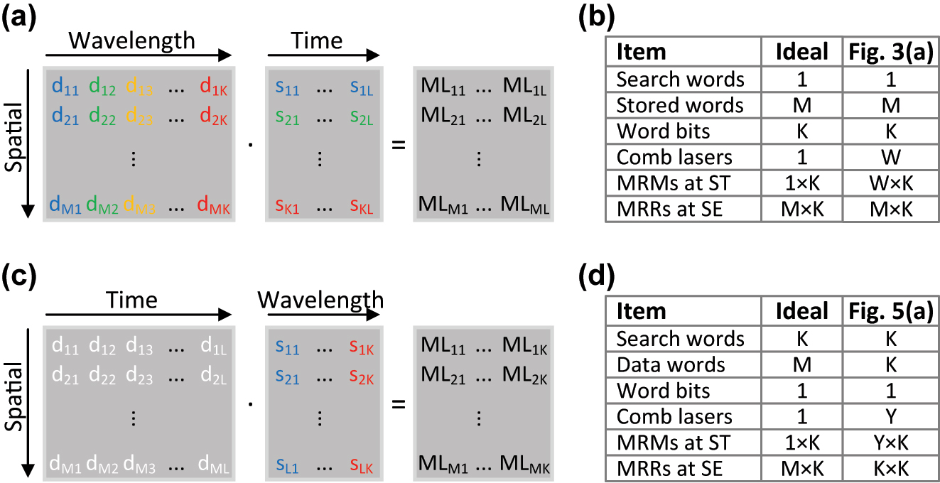
Conceptual diagrams of (a) WDM O-TCAM and (c) TDM O-TCAM architectures, which are based on matrix-matrix products. In the case of the TDM O-TCAM, the white color of the bits in the engine designated that the data words are encoded in multiple wavelengths, as shown in Figure 5(a). Scalability tables of (b) WDM O-TCAM and (d) TDM O-TCAM architectures. The total number of each of the items in the tables is determined at a single clock cycle.
![Figure 3:
Microring-based WDM O-TCAM architecture. (a) A block diagram of the proposed architecture. (b) A schematic of one of the SiPh MRM-based transmitter circuits, located in the Search Transmitter. (c) A schematic of a MLs circuit with splitter size of 1 × 2, as an example, located in the Search Engine. m and (m + 1) are the indexes of the MLs, where m ∈ [1, M − 1]. GC, OEC, and DD are acronyms of grating coupler, optoelectronic conversion, and decision device.](/document/doi/10.1515/nanoph-2023-0406/asset/graphic/j_nanoph-2023-0406_fig_003.jpg)
Microring-based WDM O-TCAM architecture. (a) A block diagram of the proposed architecture. (b) A schematic of one of the SiPh MRM-based transmitter circuits, located in the Search Transmitter. (c) A schematic of a MLs circuit with splitter size of 1 × 2, as an example, located in the Search Engine. m and (m + 1) are the indexes of the MLs, where m ∈ [1, M − 1]. GC, OEC, and DD are acronyms of grating coupler, optoelectronic conversion, and decision device.
We simulated in Lumerical INTERCONNECT a 2-bit WDM O-TCAM, which allows us to execute a single symbol content search at each clock cycle, to demonstrate the operation of the proposed architecture in the time-domain. We modelled a Search Transmitter with two cascaded PIN MRMs and a Search Engine with two cascaded microring filters, where an APD is placed at the through port of the second ring. This allows us to map all the combinations listed in Table 1 through three experiments, where the search sequence is X01XX, a six words series, and the stored word is 0, 1, or X. The most- and least-significant bit sequences, s1(t) and s2(t), both construct the search words series, have a pulse shape of non-return-to-zero (NRZ) with rise and fall periods of 30 % of the bit duration and data rate of 10 Gbps. The first and second MRMs are driven by s1(t) and s2(t), respectively. The model of the MRMs is taken from the process design kit (PDK) we developed, as part of the Exascale Computing Project, for our research on exascale computing interconnects [13, 26, 27]. The driving signals, s1(t) and s2(t), are shown in Figure 4(a). The power of each of the laser lines is set to −6 dBm and the resonances of the first and second MRMs are 1309.2 and 1309.8 nm, respectively, and their Q and extinction ratio (ER) are 15 K and 13 dB. The Q and ER of the Search Engine rings, which operate as notch filters, were selected to be 6 K and 15 dB to ensure high attenuation of the transmitted modulated light at a Match state, which leads to high-contrast between Match and Mismatch states. In both the transmitter and engine, the amplitude of ‘1’ is 0.95 V, which results in resonance shift of 0.3 nm. The match signal, ϕ d (t), where the subscript d is the value of the stored word, is measured at the output of the APD [22] from our exascale PDK. The comparison results between the search sequence and the stored word are shown in Figure 4(b) (d = 0), 4(c) (d = 1), and 4(d) (d = X). The match signals (continuous) are shifted by τ to compensate for the delay resulting from the APD. The results show that in the three cases the match signal follows the decision scheme in Table 1 as expected. Moreover, the contrast between Match and Mismatch states depends on the ER of the ring filters, specifically the small APD current at Match state is minimized when all the rings block the light of all search bits as shown for d = X.

The simulation results of a two-bit WDM O-TCAM circuit. (a) The first and second search bit signals, s1(t) and s2(t). The search sequence is indicated above the search signals. (b)–(d) The shifted match signal (continuous) at the APD output, when compared to a stored symbol of 0 (subplot b), 1 (subplot c), or X (subplot d). The Mismatch states are indicated above the shifted match signals.
2.2 TDM O-TCAM
The TDM O-TCAM architecture utilizes as well a cascaded SiPh microrings structure to execute a matrix-matrix multiplication, where the bits of the search and data words are time-encoded, as shown in Figure 2(c). The white color of bits indicates that in the proposed design each of the search words is compared with all the data words at the engine. A block diagram of the proposed TDM O-TCAM is shown in Figure 5(a), where the search dimensions and devices count are listed in the table shown in Figure 2(d). The number of channels, which determined by the FSR and channel spacing, sets the word count. Therefore, the Search Transmitter distributes simultaneously K search words towards the Search Engine, which in turn compares these words with K data words. The number of data words can be increased beyond K by attaching additional Search Engine units. Each pair of bits in the search and data words represent a symbol as defined in Table 1. Similarly to the WDM O-TCAM architecture, the Search Transmitter and Search Engine consist of

MRM-based TDM O-TCAM architecture. (a) A block diagram of the proposed architecture. (b) A schematic of one of the SiPh MRM-based transmitters, located in the TDM Search Transmitter. (c) A schematic of the 1-st and 2-nd cascaded MLs circuit, located in the TDM Search Engine. The bar above di,j indicates inverted bit value, required to accommodate the enecoding scheme when the match signal is measured at the microring drop port. GC, OEC, and DD are acronyms of grating coupler, optoelectronic conversion, and decision device.
To demonstrate the time-domain operation, we simulated in Lumerical INTERCONNECT a TDM O-TCAM circuit, where its Search Transmitter and Search Engine have a single PIN MRM, taken from our exascale PDK. The resonance, Q, and ER of these MRMs are 1309.5 nm, 15 K, and 13 dB. The power of the laser, which is connected to the input of the MRM of the Search Transmitter, is −6 dBm. The search and data sequences are 000111XX and 01X01X01, respectively, which allows us to map all the combinations listed in Table 1. The search signal, s(t), and data signal, d(t), have data rate of 10 Gbps and pulse shape of NRZ with amplitude of 1 V and rise and fall periods of 30 % of the bit duration. The search and data signals are shown in Figure 6(a) and (b), respectively. The match signal, ϕ(t), is measured at the output of our APD [22] and connected to the drop port of the MRM located at the Search Engine. The match signal is shown in Figure 6(c). We shifted ϕ(t) by τ to compensate for the delay resulting from the APD. The match signal in this experiment follows the decision scheme in Table 1 as expected. The small spikes that can be observed at the Match state are due to the dynamic of light within the microring cavity.

The simulation results of a TDM O-TCAM circuit of a single search word and a single data word. (a) The search signal, s(t). The search sequence is indicated above of the signal. (b) The data signal, d(t). The data sequence is indicated above of the signal. (c) The shifted match signal (continuous) at the APD output. The Mismatch states are indicated above of the shifted match signal.
3 Experimental demonstration
We validated the operation of the proposed WDM and TDM O-TCAM architectures through proof-of-concept experiments. In these experiments, we used a test structure of two cascaded MRMs located on a SiPh wafer that was manufactured in CEA-LETI [28]. A photo of this device is shown in Figure 7(a), where the MRMs parameters are specified in the table. The setup for the analysis of the WDM O-TCAM design is shown in Figure 7(b). In this experiment, the cascaded microrings circuit operates as a 2-bit Search Engine, where the voltages applied by the DC sources set the data to store, i.e., 0, 1, or X. The lines at 1322.12 and 1323.1 nm, which are generated by the tunable laser sources (TLSs), each with power of 6 and 8 dBm, respectively (due of the unbalanced system losses), are being externally modulated by a preset sequence of 2-bit search words using 40 GHz Intensity Modulator[1] (IM). The use in external modulators is a compromise aimed to demonstrate the proposed microring-based WDM O-TCAM architecture, which requires four microrings for 2-bit design, with the available test structure of two cascaded microrings. The 3.984 Gbps search sequence of X01XX is being generated by an 65 GSa/s arbitrary waveform generator[2] (AWG). Each of the search signals, s1(t) and s2(t), is measured at the output of an external PD[3] connected to the exit port of the SiPh circuit by a real-time oscilloscope[4] (RTO) when the microrings are off-tuned. These measured signals are shown in Figure 8(a). The match signals, ϕ d (t), for d = 0, d = 1, and d = X are shown in Figure 8(b)–(d), respectively. In all three cases, the match signal follows the decision scheme presented in Table 1.

Proof of concept of the proposed O-TCAM architectures. (a) The two cascaded MRMs device, which was manufactured in CEA-LETI. (b) The experimental setup of the 2-bits WDM O-TCAM architecture. (c) The experimental setup of the 1-word TDM O-TCAM architecture.

The experimental results of a 2-bits WDM O-TCAM architecture. (a) The first and second search bit signals, s1(t) and s2(t), which are measured by the RTO, and above them the search sequence is indicated. (b)–(d) The match signal, which is measured by the RTO, when compared to a stored symbol of 0 (subplot b), 1 (subplot c), or X (subplot d). The Mismatch events (post analyzed, threshold
In the experiment of the TDM O-TCAM design, the first MRM operates as a 1-word Search Transmitter and the second MRM operates as a 1-word Search Engine. The setup is shown in Figure 7(c), where the MRMs are tuned to 1323.1 nm and the same AWG, PD, and RTO are used. The search sequence of 000111XX and data sequence of 01X01X01, respectively, are generated by the AWG and beat at 3.03 Gbps. The measured search and data signals, which are measured at the output of the PD by a RTO when the microrings are off-tuned, are shown in Figure 9(a) and (b). Afterwards, we compared the search and data signals using the 1-word TDM O-TCAM setup. The match signal, ϕ(t), is shown in Figure 9(c), and it can be observed that the received signal follows the decision scheme in Table 1.

The experimental results of a 1-word TDM O-TCAM architecture. (a) The search signal, s(t), measured at the RTO, and above it the search sequence. (b) The data signal, d(t), measured at the RTO, and above it the data sequence. (c) The match signal, ϕ(t), measured at the RTO. The events corresponding to a Mismatch state (post analyzed, threshold
4 Noise analysis
The size of the proposed O-TCAM architectures is limited by the FSR and the noise. While the FSR determines the maximum number of wavelength channels, K, the noise, on the other hand, dictates both the number of channels and the splitter degree, N, which allow us in the proposed architectures to share the energy cost of the drivers and heaters of the Search Transmitter. Specifically, the noise determines the required number of photons at the PD to achieve a specific signal to noise ratio (SNR) that guarantees the match decision quality, similar to how SNR determines the bit error rate (BER) in Datacom interconnects. The photon count, after taking into account the link losses, determines the maximum values of N and K, i.e., splitter size and microring count, at given comb line power. We evaluate here the scaling limitation of the proposed O-TCAMs due to noise, using similar methodology as in [29], which was developed for matrix-vector multiplication. At the full-scale of the WDM O-TCAM we have a matrix of W × K of stored words multiplied with a search word matrix of K × L, whereas in the TDM O-TCAM we have a multiplication between data word matrix of K × L and search word matrix of L × K. As our interest here is in a case study of matrix-vector product, we degenerated the WDM O-TCAM to a single clock cycle, i.e., a search word matrix of K × 1, and set the stored word matrix to N × K, which focuses the scaling evaluation on a single engine circuit of N stored words, enabled by the 1 × N splitter at its input. A similar simplification is done for the TDM O-TCAM—the Search Transmitter transmits a data word vector of L × 1 and the data matrix at the engine has a size of N × L. This is carried out by modulating N data words over the same resonance wavelength as the search word, which is allowed because of the spatial multiplexing enabled by the 1 × N splitter. To simplify the notation in the following model, we designate D as the number of symbols within a word, i.e., for WDM O-TCAM
Given the photon count in a unit interval of a search bit is
where the matrix
where
where nMAC,1 is the number of photons for a single multiply-accumulate (MAC) operation, when a single mismatch event occurred and after considering the link losses. Because the electrical SNR scales with the square of the photocurrent, the SNR can be written as:
This result shows that the electrical SNR scales with nMAC,1HM,i, which means that the SNR is effected not only by the number of photons through the link budget performance, but also by the Hamming distance. Moreover, we designate the number of photons for no mismatch events and one mismatch event within the match signal as Φi,0 and Φi,1, which is equal to nMAC,1. Because max HM,i = D, then max Φ i = Φi,1D, however, a single mismatch event is already sufficient to lead to a Mismatch state for the full word, therefore the decision threshold is placed between Φi,0 and Φi,1.
This analysis describes the impact on the SNR performance due to shot noise, however, in case that non-avalanche mode of operation is considered for the APDs used in our exascale SiPh PDK, other noise mechanisms, such as TIA thermal noise, should be added in order to evaluate the link budget and specifically the required comb line optical power [29, 33]. Nonetheless, the conclusion of this paragraph that the decision threshold for a Match/Mismatch of a word lies between Φi,0 and Φi,1 still holds, and we can use the sensitivity of the APDs as a baseline to which the desired signal strength needs to be compared to obtain a certain BER, which will in turn determine how many photons are required at the laser. This is the procedure we will apply in the energy consumption discussion in the next section.
5 Energy analysis
The power consumption in the proposed designs happens in the comb source, drivers, microring heaters, OECs, and DDs. In the case of the TDM O-TCAM architecture, an additional local memory is required to store the data words. This can be done with DRAM, but due to its high access energy consumption of tens of pJ/bit [34], an energy efficient alternative would be SRAM, which consumes only a few fJ/bit. A 1 fJ/bit SRAM was demonstrated [35] at 10 MHz. An SRAM with much faster access speed of 935 MHz was shown in Ref. [36], but has energy consumption of 32.5 fJ/bit. Assuming that l × K bits of the K data words, which are loaded into the drivers of the search engine, are retrieved in parallel from the SRAM memory, the
where Pcl is the minimal optical power of a comb line that is required to detect a Match/Mismatch at the PD (see SNR discussion in Section 4) and depends on the losses in the optical link between the laser and PD, e.g., excess losses of encountered splitters and insertion loss of microrings.
where
In the case of TDM O-TCAM, we perform similar simplification as in Section 4, where the Search Transmitter transmits an L-bit data word, which is being compared with N data words of a length of L bits, where L is an index of a clock cycle. Then the energy consumption of the TDM Search Engine, after normalizing over the number of bits, number of words, and decision speed, is:
As we have here a single search word transmission then only one comb line is required. Moreover, the Match/Mismatch decision for TDM O-TCAM can be done in principle at the end of the comparison sequence, i.e., at speed of
where Pmr includes the average power required to read from the SRAM and update a FF memory unit with a new bit of a data word.
First, in our silicon photonics platform
Second, for the TDM O-TCAM architecture, the powers of peripheral electronic circuits, i.e., TIA, comparator, and integrator, embedded in the OEC and DD devices are not shared between multiple bits as occurs for the WDM O-TCAM architecture. While the number of detected photons required to make an accurate decision will be similar for both WDM and TDM schemes, and consequently will not significantly change the required photon energy in each architecture, without dedicated adjustments of the electronic peripherals to the lower bandwidth requirements for the TDM architecture, where a Match/Mismatch only needs to be communicated at
5.1 Energy estimation
The power consumption of the comb laser depends on the link insertion loss and the APD sensitivity. The SiPh components of the Search Transmitter and Search Engine are shown in Figure 3(b)–(c) for the WDM O-TCAM and in Figure 5(b)–(c) for the TDM O-TCAM. The insertion loss analysis is based on the design rules and performance of our exascale PDK. For readers convenience, key performance, which are used in the estimation of the energy consumption, of our PDK as well as supplemental decision-related devices are listed in Tables 2 and 3, respectively. The light of the comb source is coupled through a 2D grating coupler (GC), which interfaces with a 2000 μm medium-etch single mode (MESM) waveguide. The minimum loss and 1 dB bandwidth of the 2D GC is 2.6 dB (at 1310 nm) and 20 nm. Advanced design techniques, such as adjoint method-based shape optimization, are expected to improve the performance of 2D GC even further [43]. In the Search Transmitter and Search Engine, MRMs with FSR of 13.6 nm are cascaded along a deep-etch single mode (DESM) waveguide, where the channel spacing is 0.6 nm to ensure minimal crosstalk penalties in this very first performance analysis of O-TCAMs. In the future more detail analysis is required to study the impact of the channel crosstalk on the decision quality of the match signal, which can be estimated using similar methodology as in Ref. [44] or model-based simulation. We use PIN MRMs in our designs, where their through and drop ports losses are 0.1 and 3 dB, respectively. The pitch between the edge of DESM waveguide and its adjacent MRM, p1, is 15 μm, and the pitch between two adjacent MRMs, p2, is 225 μm. The losses of the MESM and DESM waveguides and medium-etch deep-etch (MEDE) taper are 1, 2 dB/cm, and 0.1 dB. The modulated light is transferred through a fiber array towards the Search Engine. Arrays of 1D GCs, which interface with a 50 μm MESM waveguide, and 2D GCs couple the light to and from the fiber array. The minimum loss and 1 dB bandwidth of 1D GC, where the light incidence angle is 0°, is 1.8 dB (at 1309 nm) and 21 nm. Better GC performance is achievable with larger incidence angle [45, 46]. In our analysis, the losses of the 1D and 2D GC connectors are 0.9 [46] and 1.8 dB, which we expect to be achievable in the near future. An optional N-way splitter, which is based on cascaded 1 × 2 multi-mode interferometer (MMI) that interfaces with MESM waveguide, is located at the front-end of the Search Engine to share the energy cost of the drivers and heaters of the Search Transmitter with multiple cascaded MRMs rows. The excess loss of our 1 × 2 MMI is 0.2 dB. The insertion loss performance of the Search Transmitter and Search Engine for the WDM and TDM schemes are summarized in Figure 10(a) and (b), respectively. The vertical red dashed line marks the FSR limit.
Key performance of HPE exascale SiPh PDK.
| Element | Parameter | Value |
|---|---|---|
| GC (1D, 0°) | Minimum lossa | 1.8 dB |
| Bandwidth (1 dB) | 21 nm | |
| Connector loss | 0.9 dB | |
| GC (2D) | Minimum lossb | 2.6 dB |
| Bandwidth (1 dB) | 20 nm | |
| Connector loss | 1.8 dB | |
| MRM (PIN) | FSR | 13.6 nm |
| Thru port loss | 0.1 dB | |
| Drop port loss | 3 dB | |
| MMI (1 × 2) | Excess loss | 0.2 dB |
| MESM waveguide | Loss | 1 dB/cm |
| DESM waveguide | Loss | 2 dB/cm |
| MEDE taper | Loss | 0.1 dB |
| Comb laser | WPE | 5 % |
| Excess power | 20 % | |
| Driver | Powerc | 6.075 mW |
| Heater | Thermal tuning efficiency | 20 mW/FSR |
| TIA | Energy efficiency | 40 fJ/bit |
| APD | Sensitivityd | −22 dBm |
-
aMinimum loss is at 1309 nm. bMinimum loss is at 1310 nm. c1-tap pre-emphasis in a 28 nm CMOS process. dAt TIA settings of 5 KΩ and 1 μA equivalent noise.
Energy performance estimation of decision-related devices.
| Element | WDM O-TCAM | TDM O-TCAM |
|---|---|---|
| Comparator | 243 fJ/bita |
|
| Integrator | 90 fJ/bitb |
-
For R b = 10 Gbps. aStrong-arm latch comparator in a 28 nm platform, where VDD = 0.9 V and C P,Q , C X,Y ≤ 200 fF. bOpAmp with feedback capacitor is expected to consume 1 mA with 0.9 V.

The end-to-end insertion loss of (a) a SiPh MRM-based transmitter, located in the WDM Search Transmitter (ST), and a SiPh MRM-based ML, located in the WDM Search Engine (SE) with single input, N = 2, or N = 4 as well as (b) a SiPh MRM-based transmitter, located in the TDM Search Transmitter, and a SiPh MRM-based cascaded ML, located in the TDM Search Engine with single input, N = 2, or N = 4.
In the determination of the required optical power of a single comb line, an APD from our exascale PDK was used followed by a TIA with gain of 5 KΩ and equivalent noise of 1 μA that translates to −22 dBm of required optical power at the APD input, which in SiPh Datacom/HPC interconnects corresponds to a BER of 10−12 [22]. The required optical power of a comb line, after considering the link insertion loss and OEC performance, for the WDM and TDM configurations, where the Search Engine has a set of one, two, or four K cascaded MRMs, are shown in Figure 11. The horizontal red dashed line at 0 dBm marks the power upper limit, which was selected to provide enough margin from the non-linear regime of the SiPh elements. The analysis shows that the splitter size is limited to 1 × 2, therefore at least

The required optical power of a comb line of (a) WDM Search Transmitter with single input, N = 2, or N = 4 as well as (b) TDM Search Transmitter with single input, N = 2, or N = 4.
At a channel data rate of R b = 10 Gbps, the energy consumption of the Search Transmitter and Search Engine variations are shown in Figure 12. In both architectures, the energy consumption of the Search Transmitter is significant due to the comb and drivers needed for the electro-optic conversion in current optical interconnect systems, which are tailored for E-CAMs. In the future, once all-optical interconnect systems, designed to be fully compatible with O-CAMs, are available the search signal can be extracted directly from the optical data stream, making the Search Transmitter redundant. The difference in the energy consumption of the Search Transmitter is a result of the different comb line power requirements between the two architectures, which is expected to be solved by engineering microrings with lower drop port losses. In the case of the WDM architecture, the energy cost of the Search Engine decreases as the length of the word increases, due to the reduction in contribution of the TIA and comparator to the total energy consumption, as predicted by the model in Eq. (6) and demonstrated in Figure 13(a) for K ∈ {8, 16, 32}. Significant reduction in this energy is expected in the near future, once the non-volatile microrings are mature to be included in our SiPh component library [23], thus making the thermal tuning redundant. Then the O-TCAM energy cost will be dependent only on the OEC and DD energy consumption divided by the channel count, and as a result our design will become competitive with low-energy E-TCAM designs [8, 49]. In the energy consumption of the TDM O-TCAM we assumed a word with 48 bits, as the length of an Ethernet MAC address. Therefore, L = 96 for the TCAM encoding scheme used in this work, which reduces the comparator energy consumption by the same factor, while the energy cost of the memory, driver, heater, TIA, and integrator is not affected by the word length as they operate at R b . This leads to Search Engine energy consumption of 1741.6 fJ/sym for ternary scheme (870.8 fJ/sym for binary scheme with L = 96). As predicted, the energy consumption of the TDM Search Engine is significantly higher than the WDM design, a result of the much higher driving power and microring drop loss as well as the mode of operation of the PD and DD. Moreover, as demonstrated in Figure 13(b) for a TDM O-TCAM architecture with L ∈ {8, 16, 32}, the driver substantially increases the total Search Engine energy consumption compared to the other engine devices. As discussed before, the energy cost of the proposed TCAM O-TCAM architecture can be reduce with design improvements in the microring, PD, and DD circuitry. However, the power arises from the multiple drivers, which are used to re-modulate each of the bits of the data words, cannot be mitigated in this specific instantiation of the TDM scheme and requires an alternative engine design, which will be presented in Section 5.2.
The energy consumption, excluding the SRAM and memory buffer for the TDM Search Engine, of the Search Transmitter (ST) and Search Engine (SE) of the (a) WDM O-TCAM as well as (b) TDM O-TCAM architectures. The channel count is equal to the number of cascaded microrings along a bus waveguide. In the case of WDM O-TCAM, each MRR stores one of the word bits, and in the case of the TDM O-TCAM, each MRM is being driven by one of the data words.

The contributions to energy efficiency from individual components of the Search Engine of the (a) WDM O-TCAM as well as (b) TDM O-TCAM architectures for various word bit count.
5.2 Alternative energy-focused TDM O-TCAM design
The proposed TDM O-TCAM architecture does not require serial-to-parallel word conversion, allows quick data word update, and has no FSR constraint on the word length, features in which the TDM scheme has an advantage over the WDM O-TCAM. However, the significant power consumed by the multiple drivers at TDM Search Engine limits its attractiveness compared to other CAMs. To address this energy burden, we propose here an alternative O-TCAM engine design that is inspired by the TDM schemes for AI applications in Refs. [44, 50]. Other photonics matrix-vector product architectures, e.g., free-space-based system [29], potentially offer better insertion loss scaling as a function of matrix size, but we focus here on pure integrated approach. A block diagram of the new Search Engine is shown in Figure 14(a). The search in this engine diagram is executed horizontally, i.e., wavelength domain, while in previous TDM scheme shown in Figure 5(a), the search is carried out vertically, i.e., spatial domain. Due to this modification, a row of cascaded MRMs can be replaced with a Mach-Zehnder modulator (MZM), which is driven by one data word, thus simplifying the electronic circuitry and considerably reducing the memory and driving energy cost. An example of sub-engine circuit is shown in Figure 14(b). After the K wavelength-encoded search words are multiplied by a data word through the re-modulation step, the results are demultiplexed and converted to electrical signal by cascaded microring filters followed by a PD. The matching state of each of the signals is determined by the DD. Therefore, for the alternative TDM O-TCAM design the energy consumption in Eq. (8) can be modified as:
where we assumed non-volatile MRRs for the demultiplexing. Similarly to the discussion in Section 5.1, SPADs can be used in this architecture for the OEC step, therefore, the match state can be determined at the end of the search sequence by a comparator. Idling the comparator for most of the match signal duration is expected to reduce the decision energy by a factor proportional to L, leading to a competitive energy consumption compared to the decision device in the WDM scheme. Furthermore, the power required to drive an MZM [51, 52] is higher than microring, however, the driving search energy in the new TDM architecture is reduced by a factor of K because one data word re-modulates K search words. Therefore, to fully leverage the energy saving potential of this TDM scheme, the number of words should be as high as possible, which can be achieved by using a wide-band comb laser with numerous lines [20], though, in this case the channel crosstalk and microring FSR constraints on the word count should be addressed. Cascading multiple stages of low-loss deinterleavers [53, 54] can alleviate the channel crosstalk. Moreover, by designing the comb line spacing such that the interference between the deinterleaved comb lines in different FSR sets is minimized, the effective transmission bandwidth can be increased significantly. As a result the total energy consumption of the new MZM-based TDM scheme is expected to be much lower than the non-volatile microring-based TDM architecture, but still higher than the WDM engine, unless additional methods can be found that reduce the driving power,

MZM-based TDM O-TCAM Search Engine architecture. (a) A block diagram of the alternative Search Engine architecture, where its core-operations of comparison and de-multiplexing are performed by the SiPh MZM and microring filters, respectively. (b) An example of pair of sub-engines, where the demultiplexer (DeMux) is based on add-drop microring filters. At the microring drop port the match signal is converted to electrical signal by the OEC and then the Match state is determined by the DD.
5.3 Energy performance comparison
To put our results in perspective, we compared the energy performance of our O-TCAM architectures with state-of-the-art E-TCAM and O-TCAM designs. Because competitive E-CAMs and O-CAMs report only on the engine performance, here, to compare apples to apples, we included only the engine-side. Moreover, it is worth to point out that the theoretic proposal of the WDM O-BCAM circuit proposed in Ref. [16] included an optimistic estimate of the minimal power consumption of such O-BCAMs to be 4.5 aJ/sym. based on the required optical power received at the PD at SNR = 1 for signal bandwidth of 50 GHz, which is linked to the laser power at the transmit-side (not yet including wall-plug efficiency of the laser, neither incorporates the effect of the link budget due to the losses in the passive devices between laser and PD). In contrast, for the comparison in this paper, we focus on the engine-side, i.e., the power related to the engine’s tuning of optical devices as well as required electronic circuitry, such as TIA and the comparator. Table 4 summarizes the comparison results between various TCAM engines. In the case of the WDM architecture, at a word length of 11 symbols, the energy consumption per ternary symbol is 290.4 fJ/sym, which is 2× the energy per channel, i.e., 145.2 fJ/channel at K = 22, because of the two-bit encoding scheme presented in Table 1. Note that when only O-BCAM functionality is required, following the proposed circuit in Ref. [16] where a single microring blocks light in one out of two incoming wavelength channels, the number of required microrings can be reduced by a factor 2, and the energy per symbol becomes 145.2 fJ/sym. When non-volatile microring are considered, the post-fabrication thermal tuning and thermal bit storing are redundant, which result in a power saving of 1.324 mW per heater, i.e., energy consumption of 25.8 fJ/sym (12.9 fJ/sym) for ternary (binary) symbol, an energy improvement by a factor of 11 compared to SiPh MRR-based WDM O-TCAM engine. In the case of the proposed MRM-based TDM O-TCAM engine, the energy consumption is 1741.6 fJ/symf for ternary symbols (see Section 5.1), six times higher compared to WDM O-TCAM engines. A significant reduction in the energy consumption of the TDM O-TCAM engine can be achieved when the SiPh MRMs are replaced with a SiPh MZM, as proposed in Section 5.2. Assuming our circuit would use the driver reported in Ref. [51], which has an energy consumption of 6.6 pJ/bit at 10 Gbps, then for a comb source with 135 lines [20] the energy consumption per word is 97.8 fJ/sym (48.9 fJ/sym) for ternary (binary) symbols. Moreover, if SPADs are being used for the OEC, then the TIA becomes redundant and the comparator can operate only at the end of the sequence and consequently its energy consumption reduces by at least a factor of L, the word length. At a word length of L = 48 (L = 96), the comparator energy consumption is 5.06 fJ/sym (2.53 fJ/sym) for ternary (binary) symbols. Therefore, the total energy consumption of this architecture is 16.8 times lower compared to MRM-based TDM O-TCAM engine.
Energy performance comparison between various CAM engine technologies.
| E-TCAM | O-TCAM (O-BCAM) | |||||||
|---|---|---|---|---|---|---|---|---|
| Reference | [49] | [11] | [7] | [55] | This work | |||
| At hand | In the near future | |||||||
| WDM | TDM | WDM | TDM | |||||
| Technology | SRAM | Memristor | Memristor | InP SOA | SiPh MRR | SiPh MRM | MOSCAP MRR | SiPh MZM |
| Method | Experiment | Simulation | Experiment | Experiment | Simulation | Simulation | Simulation | Simulation |
| Search speed | 400 MHz | 1 GHz | 100 MHz | 10 Gbps | 10 Gbps | 10 Gbps | 10 Gbps | 10 Gbps |
| Energy | 0.165 fJ/sym | 0.17 fJ/sym | 2.75 fJ/sym | 300 pJ/sym (200 pJ/sym) | 290.4 fJ/sym (145.2 fJ/sym) | 1741.6 fJ/sym (870.8 fJ/sym) | 25.8 fJ/sym (12.9 fJ/sym) | 103.4 fJ/sym (51.7 fJ/sym) |
| Included elements | Driver, shifters, registers, etc. | Driver | Driver, TIA, ADC, comparator, etc. | SOA | Heater, TIA, comparator | Memory, driver, heater, TIA, comparator, integrator | TIA, comparator | Memory, driver, TIA, comparator |
| Word length | 144 sym | 36 sym | 32 sym | 4 sym | 11 sym (22 sym) | 48 sym (96 sym) | 11 sym (22 sym) | 48 sym (96 sym) |
| Hamming distance | No | No | Yes | No | Yes | Yes | Yes | Yes |
6 Conclusions
In this work, we proposed two new SiPh microring-based O-TCAMs architectures—WDM O-TCAM and TDM O-TCAM. We demonstrated the operation of the proposed architectures through circuit simulation using our exascale silicon photonics PDK as well as lab experiments using a cascaded MRMs test structure. In both the simulation and experiment, we showed that in all cases the match signal follows the decision scheme of the proposed O-TCAM designs. Based on our exascale PDK design rules and performance, we analyzed the energy consumption of the proposed WDM O-TCAM and TDM O-TCAM. The analysis shows that the energy cost of the Search Engine of the WDM O-TCAM design reduces as the word length increases towards a minimum of 290.4 fJ/sym for ternary symbols. This energy consumption can be reduced by a factor of
Acknowledgments
We would like to thank Ashkan Seyedi, Gregg Lesartre, Sudharsanan Srinivasan, Chaerin Hong, Stanley Cheung, Bassem Tossoun, and Giacomo Pedretti for the insightful discussion and support.
-
Research funding: None declared.
-
Author contributions: All authors have accepted responsibility for the entire content of this manuscript and approved its submission.
-
Conflict of interest: This work has been done during the employment of the authors at Hewlett Packard Labs, Milpitas, CA 95035, USA. As part of this work, the following patents have been issued [57–59]: US11057143B1, US11200929B1, US20220059147A1.
-
Data availability: Data sharing is not applicable to this article as no datasets were generated or analysed during the current study.
References
[1] R. S. Williams, “What’s next? [The end of Moore’s law],” Comput. Sci. Eng., vol. 19, no. 2, pp. 7–13, 2017. https://doi.org/10.1109/mcse.2017.31.Search in Google Scholar
[2] K. Asifuzzaman, N. R. Miniskar, A. R. Young, F. Liu, and J. S. Vetter, “A survey on processing-in-memory techniques: advances and challenges,” Mem. – Mater., Dev., Circ. Syst., vol. 4, 2023, Art. no. 100022. https://doi.org/10.1016/j.memori.2022.100022.Search in Google Scholar
[3] A. McAuley and P. Francis, “Fast routing table lookup using cams,” in IEEE INFOCOM ’93 the Conf. on Computer Communications, Proc., vol. 3, San Francisco, CA, USA, IEEE, 1993, pp. 1382–1391.10.1109/INFCOM.1993.253403Search in Google Scholar
[4] C. Xu, S. Chen, J. Su, S. M. Yiu, and L. C. K. Hui, “A survey on regular expression matching for deep packet inspection: applications, algorithms, and hardware platforms,” IEEE Commun. Surv. Tutorials, vol. 18, no. 4, pp. 2991–3029, 2016. https://doi.org/10.1109/comst.2016.2566669.Search in Google Scholar
[5] G. Pedretti, C. E. Graves, S. Serebryakov, et al.., “Tree-based machine learning performed in-memory with memristive analog CAM,” Nat. Commun., vol. 12, no. 1, p. 5806, 2021. https://doi.org/10.1038/s41467-021-25873-0.Search in Google Scholar PubMed PubMed Central
[6] K. Ni, X. Yin, A. F. Laguna, et al.., “Ferroelectric ternary content-addressable memory for one-shot learning,” Nat. Electron., vol. 2, no. 11, pp. 521–529, 2019. https://doi.org/10.1038/s41928-019-0321-3.Search in Google Scholar
[7] R. Mao, B. Wen, A. Kazemi, et al.., “Experimentally validated memristive memory augmented neural network with efficient hashing and similarity search,” Nat. Commun., vol. 13, 2022, Art. no. 6284. https://doi.org/10.1038/s41467-022-33629-7.Search in Google Scholar PubMed PubMed Central
[8] C. Li, C. E. Graves, X. Sheng, et al.., “Analog content-addressable memories with memristors,” Nat. Commun., vol. 11, 2020, Art. no. 1638. https://doi.org/10.1038/s41467-020-15254-4.Search in Google Scholar PubMed PubMed Central
[9] A. Kazemi, S. Sahay, A. Saxena, M. M. Sharifi, M. Niemier, and X. S. Hu, “A flash-based multi-bit content-addressable memory with euclidean squared distance,” in 2021 IEEE/ACM International Symposium on Low Power Electronics and Design (ISLPED), Boston, MA, USA, IEEE, 2021, pp. 1–6.10.1109/ISLPED52811.2021.9502488Search in Google Scholar
[10] S. George, N. Jao, A. K. Ramanathan, et al.., “Integrated CAM-RAM functionality using ferroelectric FETs,” in 2020 21st International Symposium on Quality Electronic Design (ISQED), Santa Clara, CA, USA, IEEE, 2020, pp. 81–86.10.1109/ISQED48828.2020.9136998Search in Google Scholar
[11] C. E. Graves, C. Li, X. Sheng, et al.., “Memristor TCAMs accelerate regular expression matching for network intrusion detection,” IEEE Trans. Nanotechnol., vol. 18, pp. 963–970, 2019. https://doi.org/10.1109/tnano.2019.2936239.Search in Google Scholar
[12] Y. London, T. Van Vaerenbergh, A. J. Rizzo, et al.., “Energy efficiency analysis of comb source carrier-injection ring-based silicon photonic link,” IEEE J. Sel. Top. Quantum Electron., vol. 26, no. 2, pp. 1–13, 2020. https://doi.org/10.1109/jstqe.2019.2934121.Search in Google Scholar
[13] Y. London, T. Van Vaerenbergh, L. Ramini, et al.., “Performance requirements for terabit-class silicon photonic links based on cascaded microring resonators,” J. Lightwave Technol., vol. 38, no. 13, pp. 3469–3477, 2020. https://doi.org/10.1109/jlt.2019.2961455.Search in Google Scholar
[14] S. Pitris, C. Vagionas, P. Maniotis, G. T. Kanellos, and N. Pleros, “An optical content addressable memory cell for address look-up at 10 gb/s,” IEEE Photon. Technol. Lett., vol. 28, no. 16, pp. 1790–1793, 2016. https://doi.org/10.1109/lpt.2016.2572299.Search in Google Scholar
[15] G. Mourgias-Alexandris, C. Vagionas, A. Tsakyridis, P. Maniotis, and N. Pleros, “All-optical 10gb/s ternary-cam cell for routing look-up table applications,” Opt. Express, vol. 26, no. 6, pp. 7555–7562, 2018. https://doi.org/10.1364/oe.26.007555.Search in Google Scholar
[16] Y. Alkabani, M. Miscuglio, V. J. Sorger, and T. El-Ghazawi, “OE-CAM: a hybrid opto-electronic content addressable memory,” IEEE Photon. J., vol. 12, no. 2, pp. 1–14, 2020. https://doi.org/10.1109/jphot.2020.2966748.Search in Google Scholar
[17] Y. London, T. Van Vaerenbergh, L. Ramini, et al.., “WDM ternary content-addressable memory for optical links,” in 2023 IEEE Silicon Photonics Conf. (SiPhotonics), Washington, DC, USA, IEEE, 2023, pp. 1–2.10.1109/SiPhotonics55903.2023.10141953Search in Google Scholar
[18] K. Pagiamtzis and A. Sheikholeslami, “Content-addressable memory (CAM) circuits and architectures: a tutorial and survey,” IEEE J. Solid State Circ., vol. 41, no. 3, pp. 712–727, 2006. https://doi.org/10.1109/jssc.2005.864128.Search in Google Scholar
[19] G. Kurczveil, C. Zhang, A. Descos, D. Liang, M. Fiorentino, and R. Beausoleil, “On-chip hybrid silicon quantum dot comb laser with 14 error-free channels,” in 2018 IEEE International Semiconductor Laser Conf. (ISLC), Santa Fe, NM, USA, IEEE, 2018, pp. 1–2.10.1109/ISLC.2018.8516175Search in Google Scholar
[20] G. Kurczveil, A. Descos, D. Liang, M. Fiorentino, and R. Beausoleil, “Hybrid silicon quantum dot comb laser with record wide comb width,” in Frontiers in Optics/Laser Science (2020), paper FTu6E.6, Washington, DC, USA, Optica Publishing Group, 2020, p. FTu6E.6.10.1364/FIO.2020.FTu6E.6Search in Google Scholar
[21] S. Cheung, Y. Yuan, Y. Peng, et al.., “Demonstration of a 17 × 25 gb/s heterogeneous iii-v/si dwdm transmitter based on (de-) interleaved quantum dot optical frequency combs,” J. Lightwave Technol., vol. 40, no. 19, pp. 6435–6443, 2022. https://doi.org/10.1109/jlt.2022.3196914.Search in Google Scholar
[22] Z. Huang, C. Li, D. Liang, et al.., “25 Gbps low-voltage waveguide Si–Ge avalanche photodiode,” Optica, vol. 3, no. 8, pp. 793–798, 2016. https://doi.org/10.1364/optica.3.000793.Search in Google Scholar
[23] D. Liang, S. Srinivasan, G. Kurczveil, et al.., “An energy-efficient and bandwidth-scalable DWDM heterogeneous silicon photonics integration platform,” IEEE J. Sel. Top. Quantum Electron., vol. 28, no. 6, pp. 1–19, 2022. https://doi.org/10.1109/jstqe.2022.3181939.Search in Google Scholar
[24] J. Youn, T.-C. Huang, P. Rhim, et al.., “3D-Integrated DWDM silicon photonics receiver,” in OSA Advanced Photonics Congress 2021, Washington, DC, USA, Optica Publishing Group, 2021, p. ITu4A.4.10.1364/IPRSN.2021.ITu4A.4Search in Google Scholar
[25] B. Razavi, “The strong ARM latch [A circuit for all seasons],” IEEE Solid State Circ. Mag., vol. 7, no. 2, pp. 12–17, 2015. https://doi.org/10.1109/mssc.2015.2418155.Search in Google Scholar
[26] M. A. Seyedi, J. Hulme, P. Sun, et al.., “Overview of silicon photonics components for commercial DWDM applications,” in OSA Advanced Photonics Congress (AP) 2019 (IPR, Networks, NOMA, SPPCom, PVLED) (2019), paper ITh1A.3, Burlingame, CA, USA, Optica Publishing Group, 2019, p. ITh1A.3.Search in Google Scholar
[27] L. Ramini, Y. London, D. Dauwe, et al.., “Silicon photonics I/O nodes for HPC applications,” in 2023 IEEE Photonics Society Summer Topicals Meeting Series (SUM), Sicily, Italy, IEEE, 2023, pp. 1–2.10.1109/SUM57928.2023.10224394Search in Google Scholar
[28] B. Szelag, M. A. Seyedi, S. Malhouitre, et al.., “200 mm silicon photonic platform suitable for high performance computing applications,” in 2016 IEEE 13th International Conf. on Group IV Photonics (GFP), Shanghai, China, IEEE, 2016, pp. 170–171.10.1109/GROUP4.2016.7739098Search in Google Scholar
[29] R. Hamerly, L. Bernstein, A. Sludds, M. Soljačić, and D. Englund, “Large-scale optical neural networks based on photoelectric multiplication,” Phys. Rev. X, vol. 9, no. 2, 2019, Art. no. 021032. https://doi.org/10.1103/physrevx.9.021032.Search in Google Scholar
[30] J.-S. Youn, M.-J. Lee, K.-Y. Park, H. Rücker, and W.-Y. Choi, “SNR characteristics of 850-nm OEIC receiver with a silicon avalanche photodetector,” Opt. Express, vol. 22, no. 1, pp. 900–907, 2014. https://doi.org/10.1364/oe.22.000900.Search in Google Scholar
[31] G. P. Agrawal, Fiber-Optic Communication Systems, 4th ed. John Wiley & Sons, 2010.10.1002/9780470918524Search in Google Scholar
[32] J.-S. Youn, M.-J. Lee, K.-Y. Park, H. Rücker, and W.-Y. Choi, “An integrated 12.5-Gb/s optoelectronic receiver with a silicon avalanche photodetectorin standard SiGe BiCMOS technology,” Opt. Express, vol. 20, no. 27, pp. 28153–28162, 2012. https://doi.org/10.1364/oe.20.028153.Search in Google Scholar PubMed
[33] A. N. Tait, “Quantifying power in silicon photonic neural networks,” Phys. Rev. Appl., vol. 17, no. 5, 2022, Art. no. 054029. https://doi.org/10.1103/physrevapplied.17.054029.Search in Google Scholar
[34] C. Demirkiran, F. Eris, G. Wang, et al.., “An electro-photonic system for accelerating deep neural networks,” 2022 [Online]. Available at: http://arxiv.org/abs/2109.01126.Search in Google Scholar
[35] C.-C. Wang, R. G. B. Sangalang, I.-T. Tseng, Y.-J. Chiu, Y.-C. Lin, and O. L. J. A. Jose, “A 1.0 fJ energy/bit single-ended 1 kb 6T SRAM implemented using 40 nm CMOS process,” IET Circuits, Devices Syst., vol. 17, no. 2, pp. 75–87, 2023. https://doi.org/10.1049/cds2.12141.Search in Google Scholar
[36] J. Chen, W. Zhao, Y. Wang, and Y. Ha, “Analysis and optimization strategies toward reliable and high-speed 6T compute SRAM,” IEEE Trans. Circ. Syst. I: Regul. Pap., vol. 68, no. 4, pp. 1520–1531, 2021. https://doi.org/10.1109/tcsi.2021.3054972.Search in Google Scholar
[37] S. Liu, P. Li, J. Zhang, et al.., “16.2 A 28 nm 53.8TOPS/W 8b sparse transformer accelerator with in-memory butterfly zero skipper for unstructured-pruned NN and CIM-based local-attention-reusable engine,” in 2023 IEEE International Solid-State Circuits Conf. (ISSCC), San Francisco, CA, USA, IEEE, 2023, pp. 250–252.10.1109/ISSCC42615.2023.10067360Search in Google Scholar
[38] F. Tu, Z. Wu, Y. Wang, et al.., “A 28 nm 15.59 µj/token full-digital bitline-transpose CIM-based sparse transformer accelerator with pipeline/parallel reconfigurable modes,” in 2022 IEEE International Solid-State Circuits Conf. (ISSCC), vol. 65, San Francisco, CA, USA, IEEE, 2022, pp. 466–468.10.1109/ISSCC42614.2022.9731645Search in Google Scholar
[39] A. Rizzo, Y. London, G. Kurczveil, et al.., “Energy efficiency analysis of frequency comb sources for silicon photonic interconnects,” in 2019 IEEE Optical Interconnects Conf. (OI), Santa Fe, NM, USA, IEEE, 2019, pp. 1–2.10.1109/OIC.2019.8714405Search in Google Scholar
[40] B. Tossoun, D. Liang, S. Cheung, et al.., “High-speed and energy-efficient non-volatile silicon photonic memory based on heterogeneously integrated memresonator,” arXiv, 2023 [Online]. Available at: https://arxiv.org/abs/2303.05644.10.1038/s41467-024-44773-7Search in Google Scholar
[41] F. Ceccarelli, G. Acconcia, A. Gulinatti, M. Ghioni, I. Rech, and R. Osellame, “Recent advances and future perspectives of single-photon avalanche diodes for quantum photonics applications,” Adv. Quant. Technol., vol. 4, no. 2, 2021, Art. no. 2000102. https://doi.org/10.1002/qute.202000102.Search in Google Scholar
[42] F. Gramuglia, M.-L. Wu, C. Bruschini, M.-J. Lee, and E. Charbon, “A low-noise CMOS SPAD pixel with 12.1 Ps SPTR and 3 Ns dead time,” IEEE J. Sel. Top. Quantum Electron., vol. 28, no. 2, pp. 1–9, 2022. https://doi.org/10.1109/jstqe.2021.3088216.Search in Google Scholar
[43] P. Sun, T. V. Vaerenbergh, S. Hooten, and R. Beausoleil, “Adjoint optimization of polarization-splitting grating couplers,” Opt. Express, vol. 31, no. 3, pp. 4884–4898, 2023. https://doi.org/10.1364/oe.477532.Search in Google Scholar PubMed
[44] R. Hamerly, A. Sludds, S. Bandyopadhyay, et al.., “Netcast: low-power edge computing with WDM-defined optical neural networks,” arXiv, 2022 [Online]. Available at: https://arxiv.org/pdf/2207.01777.pdf.Search in Google Scholar
[45] D. Fowler, P. Grosse, F. Gays, et al.., “Fiber grating coupler development for Si-photonics process design kits at CEA-LETI,” in Smart Photonic and Optoelectronic Integrated Circuits XXI, vol. 10922, San Francisco, CA, USA, SPIE, 2019, pp. 19–25.10.1117/12.2511845Search in Google Scholar
[46] S. Mathai, P. Rosenberg, G. Panotopoulos, et al.., “Detachable 1 × 8 single mode optical interface for dwdm microring silicon photonic transceivers,” in Optical Interconnects XX, vol. 11286, San Francisco, CA, USA, SPIE, 2020, p. 112860A.10.1117/12.2544400Search in Google Scholar
[47] W. Bogaerts, P. De Heyn, T. Van Vaerenbergh, et al.., “Silicon microring resonators,” Laser Photon. Rev., vol. 6, no. 1, pp. 47–73, 2012 [Online]. Available at: https://onlinelibrary.wiley.com/doi/abs/10.1002/lpor.201100017.10.1002/lpor.201100017Search in Google Scholar
[48] P. Sun, J. Hulme, T. Van Vaerenbergh, et al.., “Statistical behavioral models of silicon ring resonators at a commercial cmos foundry,” IEEE J. Sel. Top. Quantum Electron., vol. 26, no. 2, pp. 1–10, 2020. https://doi.org/10.1109/jstqe.2019.2945927.Search in Google Scholar
[49] P.-T. Huang and W. Hwang, “A 65 nm 0.165 fj/bit/search 256 × 144 TCAM macro design for IPv6 lookup tables,” IEEE J. Solid State Circ., vol. 46, no. 2, pp. 507–519, 2011. https://doi.org/10.1109/jssc.2010.2082270.Search in Google Scholar
[50] A. Sludds, S. Bandyopadhyay, Z. Chen, et al.., “Delocalized photonic deep learning on the internet’s edge,” Science, vol. 378, no. 6617, pp. 270–276, 2022. https://doi.org/10.1126/science.abq8271.Search in Google Scholar PubMed
[51] L. Szilagyi, R. Henker, D. Harame, and F. Ellinger, “2.2-pJ/bit 30-Gbit/s mach-zehnder modulator driver in 22-nm-FDSOI,” in 2018 IEEE/MTT-S International Microwave Symposium – IMS, Philadelphia, PA, USA, IEEE, 2018, pp. 1530–1533.10.1109/MWSYM.2018.8439675Search in Google Scholar
[52] C. Li, K. Yu, J. Rhim, et al.., “A 3D-integrated 56 Gb/s NRZ/PAM4 reconfigurable segmented Mach-Zehnder modulator-based Si-photonics transmitter,” in 2018 IEEE BiCMOS and Compound Semiconductor Integrated Circuits and Technology Symposium (BCICTS), San Diego, CA, USA, IEEE, 2018, pp. 32–35.10.1109/BCICTS.2018.8551089Search in Google Scholar
[53] S. Cheung, G. Kurczveil, Y. Hu, et al.., “Ultra-power efficient heterogeneous III-V/Si de-interleavers for DWDM optical links,” in 2021 IEEE 17th International Conf. on Group IV Photonics (GFP), Malaga, Spain, IEEE, 2021, pp. 1–2.10.1109/GFP51802.2021.9673963Search in Google Scholar
[54] A. Rizzo, Q. Cheng, S. Daudlin, and K. Bergman, “Ultra-broadband interleaver for extreme wavelength scaling in silicon photonic links,” IEEE Photon. Technol. Lett., vol. 33, no. 1, pp. 55–58, 2021. https://doi.org/10.1109/lpt.2020.3044262.Search in Google Scholar
[55] C. Vagionas, P. Maniotis, S. Pitris, A. Miliou, and N. Pleros, “Integrated optical content addressable memories (CAM) and optical random access memories (RAM) for ultra-fast address look-up operations,” Appl. Sci., vol. 7, no. 7, p. 700, 2017. https://doi.org/10.3390/app7070700.Search in Google Scholar
[56] S. Aygun, M. S. Moghadam, M. H. Najafi, and M. Imani, “Learning from hypervectors: a survey on hypervector encoding,” arXiv, 2023 [Online]. Available at: http://arxiv.org/abs/2308.00685.Search in Google Scholar
[57] T. V. Vaerenbergh, C. Li, and C. Graves, “Wavelength division multiplexing (WDM)-based and multipath interferometry based optical ternary content addressable memory (TCAM),” US Patent US11 057 143B1, 2021 [Online]. Available at: https://patents.google.com/patent/US11057143B1/en.Search in Google Scholar
[58] T. V. Vaerenbergh, C. Li, and C. Graves, “Time division multiplexing (TDM) based optical ternary content addressable memory (TCAM),” US Patent US11 200 929B1, 2021 [Online]. Available at: https://patents.google.com/patent/US11200929B1/en.Search in Google Scholar
[59] T. V. Vaerenbergh, C. Li, and C. Graves, “Time division multiplexing (tdm) based optical ternary content addressable memory (tcam),” US Patent US20 220 059 147A1, 2022 [Online]. Available at: https://patents.google.com/patent/US20220059147A1/en.Search in Google Scholar
© 2023 the author(s), published by De Gruyter, Berlin/Boston
This work is licensed under the Creative Commons Attribution 4.0 International License.
Articles in the same Issue
- Frontmatter
- Research Articles
- Reconfigurable polarization processor based on coherent four-port micro-ring resonator
- Multiplexing in photonics as a resource for optical ternary content-addressable memory functionality
- Fast and accurate electromagnetic field calculation for substrate-supported metasurfaces using the discrete dipole approximation
- Robust reconfigurable radiofrequency photonic filters based on a single silicon in-phase/quadrature modulator
- A low-loss molybdenum plasmonic waveguide: perfect single-crystal preparation and subwavelength grating optimization
- Controlling coherent perfect absorption via long-range connectivity of defects in three-dimensional zero-index media
- Dynamic propagation of an Airy beam in metasurface-enabled gradiently-aligned liquid crystals
- All-dielectric metaoptics for the compact generation of double-ring perfect vector beams
- Reconfigurable nonlinear losses of nanomaterial covered waveguides
- Inverse design and optical vortex manipulation for thin-film absorption enhancement