Comparative study of all-optical INVERTER and BUFFER gates using MZI structure
-
Pallavi Singh
 ,
Ashutosh Kumar Singh
,
Ashutosh Kumar Singh

Abstract
In the paper, one input optical gates i.e., INVERTER and BUFFER have been designed using some basic assumption to analyze with the help of Semi-conductor Optical Amplifier based Mach–Zehnder Interferometer structure. The results are optimized by iterative process. The proposed design of optical gates presents low complexity, high scalability and more feasible to evaluate through digital Boolean analyzation. The digital Boolean analyzation is analyzed by some basic Boolean rules and assumptions which makes the design more digital so that it can be compatible for more than one input optical gates also. Optical Gate is designed to get constructive and destructive interference for pump and probe as they are injected into SOA simultaneously. The phase modulation is converted into intensity modulation which gives a Boolean result. The paper is optimized by Eye diagram, Q factor, wavelength spectrum and frequency chirp for both the gates. The comparative results of extinction ratio for both the gates have also been discussed. The design is supported by theoretical analysis, simulation tool (Optsim) and Boolean explanation. The proposed designs are constructed with same pattern which supports the same Boolean analysis.
1 Introduction
An optical fiber communication system is similar to any other communication system. The commercial demand for higher capacity transmission is needed to introduce a new information service and broadband service. The increase demand of bandwidth and cost are interconnected. Optical technology has succeeded in reducing the cost of bandwidth to improve the novel set of applications of bandwidth, making it more useful in behavioral pattern. The survival and improvement of optical fiber communication is based on the development of laser, amplifiers, photo detectors, switches, optical gates, optical circuits and optical devices etc. Last few decades, the research is going on to provide optical signal processing which include optical logic gates, memory elements, power limiters and pulse shapers, differential amplifiers, and A/D converters etc. All-optical logic gates are in category of ultra-fast switching device that can perform a Boolean operation in compact integration circuit [1], [2], [3]. Moreover, all optical logic gates response to light in non-linear manner to perform an optical computing where one optical data stream controls another data stream. In optical communication systems, an optical logic operation plays an essential roll to perform the optical signal processing. Now days, most of the research are diverted in the area for growing high speed optical networks. Therefore, it is essential to design an all-optical gate to avoid power consumption in opto-electronics conversion. The research is going in the field of optical logic gates is to demonstrate, ultra-high-speed optical signal processing. Many approaches have been implemented to design an optical logic gates by introducing SOA [4], [5] in waveguide, either in line or in design of MZI to produce phase modulation. Design of optical logic gates in which SOA is used, has advantage of simple implementation with large bandwidth and high-power efficiency. SOA is a single mode waveguide structure with small size, so it is easy to integrate to produce subsequent systems which are essential in optical communication [6]. For optical logic operation, a nonlinear effect is required which is introduced by SOA, making it as an excellent choice for optical switches. At low power level switching speed of SOA depends on driving power that offers potential for fast switching in picoseconds using pico-joules energy. Recent optical digital system operation is also based on digital logic design [7]. Now, to setup this technology it is important to develop basic Boolean function such as optical gates which can operate at high speed. These logic elements include the traditional Boolean logic functions operating optically such as INVERTER, BUFFER, OR, AND, NOR, XOR, NAND etc. [8], [9] and circuits such as parity checker, all-optical adder, shift registers and memory elements [10], [11], [12], [13].
Many research papers have investigated one input NOT gate with the help of different schemes [14], [15], [16]. In the paper, we have done comparative study of one input gates i.e., BUFFER and INVERTER [17], [18] with the help of two SOAs in MZI structure that made it possible to use its nonlinearity for gates. The study is also analyzed by the new optical Boolean synthesis. The switching operation of INVERTER helps to construct two inputs NOR gate as well as n-input NOR gate. Same as switching operation of Buffer helps to construct two inputs OR gate as well as n-input OR gate. The design result and analysis was supported by the opti-sim simulator and theoretical analysis.
2 Proposed model and principle
The proposed model of INVERTER/BUFFER gates, as in Figure 1 consists of a symmetrical Mach–Zehnder Interferometer (MZI) where the two SOAs are placed in series with multiplexer at the upper and lower arm of MZI. In the simulated design, the optical data (01000001001000001001) and string of (11111111111111111111)/(00000000000000000000) which is pump signal are fed in the upper and lower arms of multiplexers through CW laser to perform Boolean INVERTER/BUFFER operation. Mode lock laser (MLL) is used to generate a string of (11111111111111111111)/(01000001001000001001) which acts as a probe signal is fed into the upper arm of first 3 dB coupler. The phase shift of π/2 is produced between upper and lower arm of probe pulse traveling through it, as it is fed into the first 3 dB coupler. Pump and probe at different wavelengths are injected into SOA, so that it may operate under the gain saturated condition. As XGM occurs in SOA, available optical gain will be distributed between pump and probe wavelengths according to their photon densities. Thereby, the probe is compressed, giving the inverse effect on the gain, available to the pump wavelength. Therefore, the outputs of SOA1 and SOA2 for INVERTER/BUFFER gates with respect to the probe signal are (10111110110111110110)/(00000000000000000000) and (00000000000000000000)/(01000001001000001001) respectively. After passing through SOAs these saturated signals are fed into the second 3dB coupler, again the phase shift of π/2 is created on the probe pulse. Due to the phase modulation in MZI structure with second 3dB couplers, the total phase shift i.e., π/2 (introducer by first coupler) added to π/2 (introduced by second coupler) equals to π (at T-port) for probe signal. Therefore, if outputs of SOAs are same, it is canceled, and no pulse appears at the T-port. If it is different, then it still appears as T-port giving the INVERTER/BUFFER operation as (01000001001000001001)/(01000001001000001001).

Schematic design of all-optical INVERTER/BUFFER gate.
3 Theoretical analysis
In the proposed model, of the given design the path length (L) of two arms of interferometer is same and both signals present the same wavelength (λ). As θ 1 and θ 2 is a phase difference created by both the arms then, total phase difference created by both the arms of MZI is Δθ that can be described by
where, n1 and n2 are refractive index of both the arms of MZI. As in design, the first 3dB coupler of 50:50 coupling ratio for which
If I 1 and I 2 are intensity of light at the input terminal of MZI, which is output of Mode lock laser and MUX1 and MUX2 is intensity of light after passing through first 3dB coupler then,
After passing through SOA, due to XGM, the MLL pulse is compressed, giving the inverse effect on the gain, available to the CWL pulse. This will create the phase change in MLL pulse, so the propagation matrix is given as [20]
The transfer matrix of an MZI can be defined as
Since the second 3 dB coupler has same coupling factor, so at the output of MZI can be calculated as
As there is no signal in input 1 so, the output power at T-port and R-port is given as
where, P 1 is power at input terminal-1. From this equation we can conclude that,
At Δθ = 180° Power of T-port has maximum intensity of light and R-port has minimum. To create the optical logic gates with good performance, it is always required that for logic 0, we have to create a proper phase difference of π so that pulse is totally canceled and no power should occur at the output terminal.
4 Boolean analysis
As in digital gates, we expect the same output from the all-optical logic gates shown in Table 1. The proposed one input gates are based on XGM in SOA and XPM in MZI configuration. The design of two input gates with four case studies was mentioned in [21]
Truth table of INVERTER and BUFFER gates.
| Input (I) | INVERTER(O) | BUFFER(O) | |
|---|---|---|---|
| Case-1 | 0 | 1 | 0 |
| Case-2 | 1 | 0 | 1 |
Boolean analysis for the proposed gates is given as
Condition-1- Due to cross gain modulation (XGM) in SOA.
There will be two Rules
Rule-1- If Input probe traveling through MLL i.e., Iprobe = 0, then after passing through SOA it is multiplied to corresponding pump signal i.e., Ipump.
Rule-2- If Input probe traveling through MLL i.e., Iprobe = 1, then after passing through SOA it is added to corresponding pump signal i.e., Ipump.
Condition-2- Due to cross phase modulation (XPM) in MZI configuration.
There will be two Rules
Rule-1- After passing through SOAs, if data are same, then it will be canceled, and the output will be ‘0’ at T-port.
Rule-2- After passing through SOAs, if data are different, then it will be added, and the output will be ‘1’ at T-port.
At the upper arm of INVERTER gate Input one from CW laser, acts as a pump multiplexed with string of ones, generated from MLL laser acting as probe signal, therefore
Output of upper arm multiplexer is (I1I2) CWL. (11 12) MLL
= (0 1). (1 1)
Output of SOA1 is = {(0 + 1). (1 + 1)} as condition-1 Rule-2,
= {1.0}
At the lower arm of INVERTER gate string of ones from CW laser, acts as a pump multiplexed with string of ones, generated from MLL laser acting as probe signal, therefore
Output of lower arm multiplexer is (11 12) CWL. (11 12) MLL
= (1 1). (1 1)
Output of SOA1 is = {(1 + 1). (1 + 1)} as condition-1, Rule-2
= {0.0}
At output of second coupler T-port, according to condition-2 Rule 2&1,
{1.0}
Boolean analysis for the proposed BUFFER gate is given with the same conditions and rules discussed above.
At the upper arm of BUFFER gate Input data, I from CW laser, acts as a pump multiplexed with same Input I, generated from MLL laser acting as probe signal, therefore
Output of upper arm multiplexer is (I1I2) CWL· (I1I2) MLL
= (0 1). (0 1)
Output of SOA1 is = {(0.0). (1 + 1)} as condition-1 Rule-1&2,
= {0.0}
At the lower arm of BUFFER gate string of ones from CW laser, acts as a pump multiplexed with Input I, generated from MLL laser acting as probe signal, therefore
Output of lower arm multiplexer is (01 02) CWL. (I1I2) MLL
= (0 0). (0 1)
Output of SOA1 is = {(0.0). (0 + 1)} as condition-1 Rule-1&2,
= {0.1}
At output of second coupler T-port, according to condition-2 Rule-1&2,
{0.0}
5 Specification and method
The proposed design of optical gates presented in Figure 1, of pump signal 10 Gb/s, with peak power of 0.05 W of continuous wave. Binary sequence of 1550 nm with chirp factor 0.5 A driven by raised cosine RZ pulse is generated through PRBS. Mach–Zehnder modulator is used to modulate the signal with point per bit 25–1. Pump signal peak power, generated through CW laser is 0.015 × 10⁻⁴ W and probe signal peak power, generated through ML laser is 1 × 10⁻³ W with same PRBS at 1555 nm. Modulated Gaussian pulse, chirped with 0.5 factors driven by raised cosine RZ pulse launched into multiplexer through 3 dB coupler. After passing through both the arms of interferometer, both the arms data are merged through second 3 dB coupler at T-port to achieve the required gate output.
5.1 Simulated results and discussions for INVERTER gate
Figure 2(b) show simulated data generated through clock wave laser i.e., A = (01000001001000001001). Figure 2(a) and (c) show the string of ones generated through clock wave laser known as pump and Mode lock laser known as probe signal, respectively. The output of both multiplexers and SOAs are shown in Figure 2(d)–(g). Figure 2 (h) shows the output of INVERTER gate filtered by Lorentzian filter results at transmission port of 3 dB coupler.

Result of INVERTER Gate (a) Strings of ones from CWL at upper input arm (b) Input data from CWL at lower input arm (c) String of ones from MLL at upper input arm of MZI (d) Output of multiplexer-1 (e) Output of multiplexer-2 (f) Saturated output pulse of SOA-1 (g) Saturated output pulse of SOA-2 (h) INVERTER output at Transmission port.
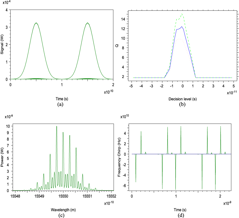
In Figure 3(a) and (b) show the eye diagram and Q-factor which has very simple structure with indistinguishable levels of marks and space. At T-port Gaussian filter is used to filter the probe pulse giving the extinction ratio 18.71 dB where the maximum Q-factor lies between −4 × 10⁻¹¹ and 4 × 10⁻¹¹ s. This shows the significant effect of noise with decision point at zero decision offset which is 20 dB. The Q-factor is very useful parameter as it is evaluated from the eye diagram. It is also common in communication system to refer Q-factor in linear unit. It was developed to address the need for a practical and accurate way of measuring the system margin and defined as linear unit of SNR for decision circuit Figure 3(c) shows the wavelength spectrum, which indicates that the highest power pulse occurs at 1555 nm with 5.9 × 10⁻⁵ W. Other two pulses of lower power are resultant of four waves mixing which are filtered by Lorentzian filter at the output. When probe and pump pass through SOA, then due to XGM, there is a phase modulation which gives raises an instantaneous change in refractive index. This creates a variation in optical frequency with time given in Figure 3(d).

Simulated result of INVERTER gate (a) Eye diagram (b) Plot of Q-factor versus decision level (c) Plot of wavelength spectrum (d) Frequency chirp.
Figure 4(a) shows the variation of ER at different data wavelengths for three different bitrates i.e., 9.0, 10.0 and 11.0 Gb/s. The extinction ratio for RZ modulation format at 9.0 Gb/s is higher than 11.0 Gb/s by 3.0 dB at 1550 nm pump wavelength as for higher bit rate resultant output is degraded. Maximum extinction ratio 19.25 dB is found at 1550 nm for 9.0 Gb/s. Figure 4(b) shows the eye pattern with color code with respect to decision time and decision level. The highest intensity of light is shown in red and lowest with pink.

Simulated result of INVERTER gate (a) Plot of extinction ratio at different wavelengths (b) Plot of eye pattern.
5.2 Simulated results and discussions for BUFFER gate
Figure 5(b) and (c) show the data generated through Clock wave laser and Mode lock laser i.e., A = (01000001001000001001). Figure 5(a) shows the string of zeros generated through Clock wave laser. Depending upon the pulse generation, these data are defined as pump and probe signals. The output of both multiplexers and SOAs are shown in Figure 5(d)–(g). Figure 5(h) shows the output of BUFFER gate results at transmission port.

Results of BUFFER gate (a) String of zeros from CWL at upper input arm (b) Input data from CWL at lower input arm (c) Input data from MLL at upper input arm of MZI (d) Output of multiplexer-1 (e) Output of multiplexer-2 (f) Saturated output pulse of SOA-1 (g) Saturated output pulse of SOA-2 (h) BUFFER output at transmission port.
In Figure 6(a) and (b) show the eye diagram and Q-factor filtered by Gaussian filter at T-port with extinction ratio 30.0 dB where the maximum Q-factor lies between −1.5 × 10⁻¹¹ and 1.5 × 10⁻¹¹ s. In eye diagram, the effect of pattern dependence is due to the laser properties as dispersion, nonlinearity, or certain noise. This problem with eye exhibiting pattern dependence is impossible to fit as a simple Gaussian distribution to either the mark or space level. Eye diagram of the received signal is important because it represents a direct measure of a system performance deprivation caused by transmission deficiency and environmental change. Figure 6(c) shows the wavelength spectrum, which indicates that the probe pulse power occurs at 1555 nm with 10.0 × 10⁻⁸ W. Wavelength spectrum at the output T-port is due to the four-wave mixing (FWM) which is analogous to intermodal distortion occurring at output signal. Other pulse at 1550 nm is a resultant of pump power which is filtered at the output. During the modulation process in SOA a time dependent phase change lead to a variation in optical frequency of the pulse at each instant given in Figure 6(d).
Sim0.ulated result of BUFFER gate (a) Eye diagram (b) Plot of Q-factor versus decision level (c) Plot of wavelength spectrum (d) Frequency chirp.
Figure 7(a) shows the variation of ER at different data wavelengths for three different bitrates i.e., 9.0, 10.0 and 11.0 Gb/s Maximum ER is obtained at 11.0 Gb/b at 1552 nm i.e., 23.64 dB. The extinction ratio higher for 9.0 than 10.0 Gb/s by the amount 0.50 dB at 1550 nm pump wavelength. Figure 7(b) shows the eye pattern of maximum intensity of light with red color with respect to decision time −5 × 10⁻¹¹–2.3 × 10⁻¹¹ s and decision level −1.1 × 10⁻⁴–1.0 × 10⁻⁴ V.

Simulated result of BUFFER gate (a) Plot of extinction ratio at different wavelengths (b) Plot of eye pattern.
6 Decisions
Extinction ratio for RZ modulation format at 10.0 Gb/s is compared in Figure 8, for Inverter and Buffer. It is seen that the extinction ratio of Buffer is higher than Inverter for the pump wavelength in the range of 1550–1553 nm because in Inverter when string of ones from clock wave laser passes through SOA, it is not totally suppressed but still some fraction of light is left out which gives the inferior extinction ratio than Buffer.
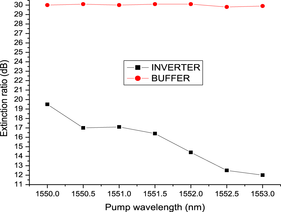
Comparative simulated results of BUFFER and INVERTER gate for extinction ratio at different pump wavelengths.
7 Scope of the work
Tremendous developments in all-optical semiconductor optical amplifier-based Mach–Zehnder Interferometer gates have been achieved in the last decade. Advance research and technological innovations have improved the design of all optical gates. Nowadays, it has become necessary to build all-optical logic gates that can be controlled optically on the same platform so that it may be easily integrated on a photonic chip. Gates that can be controlled optically are basic elements for high speed signal processing which can avoid optoelectronic conversion in communication systems. In future, all-optical logic gates are the key elements for optical signal processing such as, data encryption, address recognition and label swapping etc. The designs aim to achieve the goal through simulation and Boolean analysis in terms of gates to provide simple design rule. Still there is a vast scope to develop the memory element with the help of semiconductor optical amplifier-based Mach–Zehnder Interferometer structure. Therefore, there is broad scope for the future work in the field of all-optical digital circuit.
8 Conclusions
In the paper, we demonstrated the basic design perform all-optical INVERTER/BUFFER gates. The purpose is to get the output pulse at same wavelength for comparative study. And also develop a common Boolean rule for all-optical logic gates at same output pulse as in digital gates. Extinction ratio is a key parameter to optimize the gate operation to get a similar result as in Digital gates. In digital gates we define the gate operation if zero i.e., less than threshold voltage and one i.e., above threshold voltage. In optical gates zero, is significance of no light pulse and one is presence of light pulse. Therefore explaining optical gates with extinction ratio will make it easy to analyze and compare with digital gates. Furthermore, as we go for a higher linewidth enhancement factor, it limits the Extinction ratio to optimize the gate performance.
-
Author contribution: All the authors have accepted responsibility for the entire content of this submitted manuscript and approved submission.
-
Research funding: None declared.
-
Conflict of interest statement: The authors declare no conflicts of interest regarding this article.
References
1. Meymand, RE, Soleymeni, A, Granpayeh, N. All-optical AND, OR, and XOR logic gates based on coherent perfect absorption in graphene-based metasurface at terahertz region. Optic Commun 2020;458: 124772. https://doi.org/10.1016/j.optcom.2019.124772.Search in Google Scholar
2. Li, P, Wang, Y, Xu, P. All-optical logic gates based on unidirectional surface plasmon polaritons. Appl Optic 2019;58:4205–10. https://doi.org/10.1364/ao.58.004205.Search in Google Scholar PubMed
3. Tavakoli, G, Alipour-Banaei, H, Kashtiban, MH. A noval proposal for all-optical compact and fast XOR/XNOR gate based on photonic crystal. J Mod Optic 2019;66:599–605. https://doi.org/10.1080/09500340.2018.1559947.Search in Google Scholar
4. Webb, RP, Manning, RJ, Maxwell, GD, Poustie, AJ. 40 Gbit/s all-optical XOR gate based on hybrid-integrated Mach–Zehnder interferometer. Electron Lett 2003;39:79–80. https://doi.org/10.1049/el:20030010.Search in Google Scholar
5. Reis, C, Chattopadhyay, T, Andre, P, Teixeira, A. Single Mach–Zehnder interferometer based Boolean logic gates. Appl Optic 2012;51:8693–701. https://doi.org/10.1364/ao.51.008693.Search in Google Scholar
6. Senior, JM. Optical fiber communication. India: Pearson; 2010.Search in Google Scholar
7. Miller, DBA. Device requirement for digital optical processing in digital optical computing. SPIE Digital Libr 1990;35:68–76. https://doi.org/10.1117/12.22833569.Search in Google Scholar
8. Kim, JY, Kang, JM, Kim, TY, Han, SK. All-optical multiple logic gates with XOR, NOR,OR, and NAND functions using parallel SOA-MZI structures: theory and experiment. J Lightwave Technol 2006;24:3392–9 https://doi.org/10.1109/JLT.2006.880593.Search in Google Scholar
9. Ye, X, Ye, P, Zhang, M. All-optical NAND gate using integrated SOA-based Mach–Zehnder interferometer. Opt Fiber Technol 2006;12:312–6. https://doi.org/10.1016/j.yofte.2005.12.001.Search in Google Scholar
10. Bhattacharyya, A, Gayan, DK, Chattopadhyay, T. All-optical parallel parity generator circuit with the help of semiconductor optical amplifier (SOA)-assisted Sagnac switches. Optic Commun 2014;313:99–105. https://doi.org/10.1016/j.optcom.2013.09.042.Search in Google Scholar
11. Tsiokos, D, Kehayas, E, Vyrsokinos, K, Houbanlis, T, Stampoulidis, L, Kanellos, GT, et al. 10 Gb/s all-optacal half-adder with interferometric SOA gates. IEEE Photon Technol Lett 2004;16:284–6. https://doi.org/10.1109/lpt.2003.819394.Search in Google Scholar
12. Zhang, S, Li, Z, Liu, Y, Khoe, GD, Dorren, HJS. Optical shift register based on an optical flip-flop memory with a single active element. OSA, Opt Express 2005;13:9708–13. https://doi.org/10.1364/opex.13.009708.Search in Google Scholar PubMed
13. Lazzeri, E, Berrettini, G, Meloni, G, Bogoni, A, Poti, L. N-bits all-optical circular shift register based on semiconductor optical amplifier buffer. Proc SPIE Photon USA 2011;7948:1–6. https://doi.org/10.1117/12.873795.Search in Google Scholar
14. Lai, DMF, Kwok, CH, Yuk, HI, Wong, KKY. Picosecond all-optical logic gates (XOR, OR, NOT, and AND) in a fiber optical parametric amplifier. In: Conf OFC/NFOEC. IEEE, San Diego CA; 2008:1–3 pp.10.1109/OFC.2008.4528362Search in Google Scholar
15. Dong, J, Zhang, X, Wang, Y, Xu, J, Huang, D. 40 Gbits reconfigurable photonic logic gates based on various nonlinearities in single SOA. Electron Lett 2007;43:884–6. https://doi.org/10.1049/el:20071220.Search in Google Scholar
16. Berrettini, G, Simi, A, Malacarne, A, Bogoni, A, Potí, L. Ultrafast integrable and reconfigurable XNOR, AND, NOR, and NOT photonic logic gate. IEEE Photon Technol Lett 2006;18:917–19. https://doi.org/10.1109/lpt.2006.873570.Search in Google Scholar
17. Singh, P, Dixit, HK, Tripathi, DK, Mehra, R. Design and analysis of all-optical inverter using SOA based Mach–Zehnder interferometer. Optik 2013;124:1926–9.10.1016/j.ijleo.2012.05.038Search in Google Scholar
18. Singh, P, Tripathi, DK, Jaiswal, S, Dixit, HK. Design of all-optical buffer and OR gate using SOA-MZI. Opt Quant Electron 2013;46:1435–44. https://doi.org/10.1007/s11082-013-9856-0.Search in Google Scholar
19. Marz, R. Integrated optics. Design and modeling. Boston: Artech House; 1995.Search in Google Scholar
20. Madsen, CK, Oswald, P, Cappuzzo, M, Chen, E, Gomez, L, Griffin, A, et al. Reset-free integrated polarization controller using phase shifters. IEEE J Sel Top Quant Electron 2005;11:431–8. https://doi.org/10.1109/jstqe.2005.846538.Search in Google Scholar
21. Singh, P, Tripathi, DK, Jaiswal, S, Dixit, HK. Design and analysis of all-optical AND, XOR and OR gates basedon SOA-MZI configration. Optic Laser Technol 2015;66:35–44. https://doi.org/10.1016/j.optlastec.2014.08.002.Search in Google Scholar
© 2020 Pallavi Singh et al., published by De Gruyter, Berlin/Boston
This work is licensed under the Creative Commons Attribution 4.0 International License.
Articles in the same Issue
- Frontmatter
- Amplifiers
- Editorial
- Erbium/Ytterbium-Doped Waveguide Amplifier (EYDWA) for extended reach of Wavelength Division Multiplexing based free space optics system (WDM/FSO)
- The effect of doping on the electrons and holes in quantum dot semiconductor optical amplifiers
- Performance analysis and parameter optimization of all-optical encryption using the FWM effect in semiconductor optical amplifier
- Total gain of InTlAsSb quantum dot structures
- Gain-forming effect on optical signal-to-noise ratio in Raman fiber amplifier
- Design of EDFA based 16 channel WDM system using counter directional high pump power
- Polarization rotation-based all-optical AND gate using single semiconductor optical amplifier and implementation of a majority gate
- Performance analysis on double-pass thulium-doped fiber amplifier for 16-channel WDM system at S-band
- Design of optical packet switch in presence of dispersion compensation and amplifier noise
- Alternative method of implementation of all-optical NOR and NAND gates using quantum-dot semiconductor optical amplifiers in non-interferometer structure
- Detectors
- A long-reach radio over free space optics (Ro-FSO) system using hybrid orthogonal frequency division multiplexing (OFDM)-multibeam concept with enhanced detection
- BER performance analysis of FSO using hybrid-SIM technique with APD receiver over weak and strong turbulence channels
- High-speed and long-reach PON employing PM-DQPSK signal and coherent receiver
- Devices
- Multi-Layer Graded-Index Planar Structure for Coarse WDM Demultiplexing
- Photonic Crystal-Based All-Optical Half Adder with High Contrast Ratio
- Distributed Feedback Laser (DFB) for Signal Power Amplitude Level Improvement in Long Spectral Band
- Performance analysis of carrier depletion silicon PIN phase shifter
- Design of Optical 4 × 2 Encoder Using Cross Layered Chalcogenide2D-PC Resonator
- 1 × 2 plasmonic wavelength demultiplexer using rectangular MIM waveguide
- Compact and efficient PC-based directional coupler all-optical switch
- All-optical integrated 2-to-4 decoder and 1-to-4 demultiplexer circuit with enable using SOA based MZI
- All optical half subtractor based on threshold switching and beams interference mechanisms
- An All Optical Photonic Crystal Based XOR Gate for BPSK Signals
- Four bits data sequence generators based ytterbium doped fiber amplifiers for upgrading maximum Q factor and minimum BER
- Design and optimization of all-optical demultiplexer using photonic crystals for optical computing applications
- Hybrid buffer‐based optical packet switch with negative acknowledgment for multilevel data centers
- Application of photonic crystal based nonlinear ring resonators for realizing all optical 3-to-8 decoder
- Power conversion with complete photonic band gap in magneto-photonic crystal slab based on cerium-substituted yttrium iron garnet
- Performance comparison of all-optical logic gates using electro-optic effect in MZI-based waveguide switch at 1.46 µm
- Modelling and analysis of chirped long-period grating inscribed in a planer optical waveguide structure for sensing applications
- Comparative study of all-optical INVERTER and BUFFER gates using MZI structure
- Design of multiplexing circuit using electro-optic effect based optical waveguides
- Performance enhancement of ultra-dense WDM over FSO hybrid optical link by incorporating MIMO technique
- A novel proposal based on 2D linear resonant cavity photonic crystals for all-optical NOT, XOR and XNOR logic gates
- All optical NAND/NOR and majority gates using nonlinear photonic crystal ring resonator
- Proposed model of all optical reversible and irreversible modules on a single photonic circuit
- A photonic crystal based de-multiplexer with uniform channel spacing
- An all optical photonic crystal half adder suitable for optical processing applications
- Modelling of symmetrical quadrature optical ring resonator with four different topologies and performance analysis using machine learning approach
- Effect of misalignment on coupling efficiency in laser diode to single-mode circular core graded-index fiber coupling via cylindrical microlens on the fiber tip
- A critical review of optical switches
- An ultra-dense spacing-based PON by incorporating dual drive Mach–Zehnder modulator for comb generation
- Logic gates based on optical transistors
- Compact and ultrafast all optical 1-bit comparator based on wave interference and threshold switching methods
- A high speed all optical half adder using photonic crystal based nonlinear ring resonators
- Ultrafast all optical XOR gate using photonic crystal-based nonlinear ring resonators
- Investigating the performance of all-optical AND logic gate based on FWM effect in SOA at low power
- Nonlinear optical decoder based on photonic quasi crystal ring resonator structure
- Optical data center switches design and analysis
- Hybrid buffer and AWG based add-drop optical packet switch
- Solitons based optical packet switch analysis
- A photonic transmission link with enhanced dynamic range by incorporating phase shifters in dual drive dual parallel Mach–Zehnder modulator
- Using nonlinear ring resonators for designing an all optical comparator
- All optical half subtractor based on linear photonic crystals and phase shift keying technique
- Multi-input single-output (MISO) all optical logic (ALG) AND/NOR gate using FWM in dispersion compensation fibers in Mach-Zehnder configuration (DCF-MZI)
- Wavelength and throughput tuning of FORR-based optical filter using Sagnac effect
- Performance Enhancement of Encoding–Decoding Multidiagonal and Walsh Hadamard Codes for Spectral Amplitude Coding-Optical Code Division Multiple Access (SAC-OCDMA) Utilizing Dispersion Compensated Fiber
- Impact Analysis of the Number of Core on Hexagonal Multicore Fibre
- Effect of OPC on Fiber Nonlinearities for Dense Soliton Optical Communication Medium
- Sensing of Illegal Drugs by Using Photonic Crystal Fiber in Terahertz Regime
- On characteristic behavior and flattened chromatic dispersion properties of bent photonic crystal fibers
- Ultra high birefringent dispersion flattened fiber in terahertz regime
- Structural dependence of transmission characteristics for photonic crystal fiber with circularly distributed air-holes
- Numerical analysis of photonic crystal fibre with high birefringence and high nonlinearity
- Exploiting higher-order mode dispersion of bend M-type chalcogenide fiber in mid-IR supercontinuum generation
- Design of optoelectronic oscillator based on multiple-length single mode fiber and chirped fiber Bragg grating
- Modulation instability in nonlinear chiral fiber
- High birefringence and broadband dispersion compensation photonic crystal fiber
- Design and analysis of highly nonlinear, low dispersion AlGaAs-based photonic crystal fiber
- Highly negative dispersion compensating fiber with low third order dispersion
- Dispersion properties of single-mode optical fibers in telecommunication region: poly (methyl methacrylate) (PMMA) versus silica
- Influence of Kerr nonlinearity on group delay and modal dispersion parameters of single-mode graded index fibers: evaluation by a simple but accurate method
- Highly birefringent photonic crystal fiber with D-shaped air holes for terahertz (THz) application
- Simulation and analysis of ultra-low material loss of single-mode photonic crystal fiber in terahertz (THz) spectrum for communication applications
- Investigation of radiation induced luminescence with modulated signal transmission in optical fiber
- Design and analysis of uncoupled heterogeneous trench-assisted multi-core fiber (MCF)
- Simulative study of raised cosine impulse function with Hamming grating profile based Chirp Bragg grating fiber
- Highly Efficient Solar Energy Conversion Using Graded-index Metamaterial Nanostructured Waveguide
- Chaotic Synchronization of Mutually Coupled Lasers with Another Laser and Its Encoding Application in Secret Communication
- Passively Femtosecond Mode-Locked Erbium-Doped Fiber Oscillator with External Pulse Compressor for Frequency Comb Generation
- Conventional band demultiplexer with high quality factor and transmission power based on four optimized shaped photonic crystal resonators
- Different modulation schemes for direct and external modulators based on various laser sources
- Third order intermodulation and third order intercept in a directly modulated Fabry–Perot laser diode
- Evaluation of quantum dot light-emitting diodes synchronization under optically feedback
- Laser diode to single-mode graded index fiber coupling via cylindrical microlens on the fiber tip: evaluation of coupling efficiency by ABCD matrix formalism
- Enhanced Performance Analysis of 10 Gbit/s–10 GHz OFDM-Based Radio over FSO Transmission System Incorporating ODSB and OSSB Modulation Schemes
- An Ultra-compact Plasmonic Modulator Using Elasto-optic Effect and Resonance Phenomena
- Performance Comparison of Free-Space Optical (FSO) Communication Link Under OOK, BPSK, DPSK, QPSK and 8-PSK Modulation Formats in the Presence of Strong Atmospheric Turbulence
- Model for Performance Improvement of Blocking Probability in GMPLS Networks
- Study on P2P Service Bearer Method for Passive Optical Network for Long Distance and Wide Access
- Physical layer impairment-aware ant colony optimization approach in WDM network
- Analysis of Laser Linewidth on the Performance of Direct Detection OFDM Based Backhaul and Backbone Networks
- Radio over fiber based signal transport schemes for emerging mobile fronthaul networks – a review
- A Comparative Study of Performances Between the WDM PON System and the CWDM PON System in an Optical Access Network
- Beam divergence and operating wavelength bands effects on free space optics communication channels in local access networks
- Proactive link handover deploying coordinated transmission for indoor visible light communications (VLC) networks
- Optimized Dynamic Bandwidth Allocation Algorithm for Optical Access Networks
- Packet Blocking Performance of Cloud Computing Based Optical Data Centers Networks under Contention Resolution Mechanisms
- Optimization of an EYDWA Amplifier Parameters for a Gigabit Passive Optical Network (GPON)
- Research on Power Optimization Based on Adaptive Passive Optical Networks
- Towards cloud transport using IP-multiservices access network (MSAN)
- Enhanced redirection strategy for peer to peer services in high-speed and large-capacity ethernet passive optical networks
- Transmission challenges in metropolitan area optical networks
- Performance evaluation of a multihop WDM network with share-per-node L-WIXC architecture
- Performance analysis of hybrid optical amplifiers for multichannel wavelength division multiplexed (WDM) optical networks
- Time-domain Measurement and Analysis of Differential Mode Delay and Modal Bandwidth of Graded-Index Multimode Fiber in SDM Networks
- Seven-channel 1 Gbps TWDM coexistence architecture supporting 65 Gbps optical link for next-generation passive optical network 2–based FTTX access networks
- Link failure recovery using p-cycles in wavelength division multiplex (WDM) mesh networks
- Cascadability analysis of WDM recirculating loop buffer-based switch in optical data networks
- Evolution of optical networks: from legacy networks to next-generation networks
- A novel framework for content connectivity through optical data centers
- Performance of different hybrid dispersion compensation modules (DCMs) in long reach ultra dense WDM passive optical networks
- Performance investigation of PM-based wavelength remodulation scheme in bidirectional TWDM-PON
- Physical layer analysis of optical wireless data centers
- Novel approach to jointly optimize working and spare capacity of survivable optical networks
- A QoS provisioning architecture of fiber wireless network based on XGPON and IEEE 802.11ac
- Radio over fiber on gigabit passive optical network using QPSK modulation scheme
- Blocking performance of optically switched data networks
- Devices, communication techniques and networks for all optical communication: research issues
- Design and investigation of N1-class next-generation passive optical network-2 (NG-PON2) coexistence architecture in the presence of Kerr effect and four-wave mixing (FWM) for fiber to the home (FTTX) access networks
- Improved algorithm for enhance robustness of IPTV based on GEPON
- Simultaneous distribution of wired and two 2 × 2 MIMO wireless OFDM signals over an integrated RoF-PON system
- Analyzing optical TDMA to mitigate interference in downlink LiFi optical attocell networks
- Light fidelity optical network a comparative performance evaluation
- Theory of chaos synchronization and quasi-period synchronization of an all optic 2n-D LAN
- Performance of high scalability hybrid system of 10G-TDM-OCDMA-PON based on 2D-SWZCC code
- Performance analysis of APD and PIN diode with and without EDFA in GPON
- Improved Performance Investigation of 10 Gb/s–10 GHz 4-QAM Based OFDM-Ro-FSO Transmission Link
- Feasibility Analysis of Optical Wireless Communication for Indian Tropical and Subtropical Climates
- 40 Gb/s High-speed mode-division multiplexing transmission employing NRZ modulation format
- Performance Analysis of Shift ZCC Codes and Multi Diagonal Codes in 100 Gbps MDM-FSO System
- Combined Envelope Scaling with Modified SLM Method for PAPR Reduction in OFDM-Based VLC Systems
- Empirical Evaluation of High-speed Cost-effective Ro-FSO System by Incorporating OCDMA-PDM Scheme under the Presence of Fog
- Satellite-to-Ground FSO System Based on Multiaperture Receivers as an Optimization Solution for Strong Turbulence and Fog Conditions
- Performance analysis of NRZ and RZ variants for FSO communication system under different weather conditions
- Free space optics communication system design using iterative optimization
- Optical wireless systems with ASK & PSK using coupler-based delay line filter
- Probing of nonlinear impairments in long range optical transmission systems
- Design and Investigation of Free Space Optical System for Diverse Atmospheric Transmission Windows
- The performance comparison of hybrid WDM/TDM, TDM and WDM PONs with 128 ONUs
- Performance evaluation of a multiple optical link FSO–FSO
- Analysis the flat gain/noise figure using RAMAN-Reflective Semiconductor Hybrid Optical Amplifier in C + L + U triple band for super dense wavelength division multiplexing system
- Design improvement to reduce noise effect in CDMA multiple access optical systems based on new (2-D) code using spectral/spatial half-matrix technique
- High-speed signal processing and wide band optical semiconductor amplifier in the optical communication systems
- 2 × 20 Gbit/s OFDM-based FSO transmission system for HAP-to-ground links incorporating mode division multiplexing with enhanced detection
- Radio-over-fiber front-haul link design using optisystem
- A 2 × 20 Gbps hybrid MDM-OFDM–based high-altitude platform-to-satellite FSO transmission system
- Analysis of hybrid integrated-alternate mark inversion (I-AMI) modulation and symmetrical-symmetrical-post (SSP) dispersion compensation technique in single-tone radio over fiber (RoF) system
- Peak to average power ratio (PAPR) reduction in filter bank multicarrier (FBMC) and orthogonal frequency division multicarrier (OFDM) based visible light communication systems
- Development and performance improvement of a novel zero cross-correlation code for SAC-OCDMA systems
- Comparative analysis of SISO and wavelength diversity-based FSO systems at different transmitter power levels
- Effect of adverse weather conditions and pointing error on the performance of 2-D WH/TS OCDMA over FSO link
- Performance of LED for line-of-sight (LoS) underwater wireless optical communication system
- Underwater wireless optical communication: a case study of chlorophyll effect
- Subcarrier multiplexed radio over fiber system with optical single sideband modulation
- Performance investigation of free space optics link employing polarization division multiplexing and coherent detection-orthogonal frequency division multiplexing under different link parameters
- Performance analysis of FSO link under the effect of fog in Delhi region, India
- Design and analysis of full duplex RoF system with efficient phase noise cancellation from a coherent RoF system
- Mathematical modeling of optical impairments in DSP based WDM coherent system
- Analysis of 64 channels based IS-OWC system using different intereference reduction techniques
- Effects of local oscillator on the performance of DP-QPSK WDM system with channel spacing of 37.5 GHz
- Dual band radio-over-fibre millimetre–wave system utilizing optical frequency combs
- Full duplex dispersion compensating system based on chromatic dispersion in analog RoF links
- Performance enhancement of Raman + EYDFA HOA for UD-WDM system applications
- Crosstalk characterization in homogeneous multicore fiber using discrete changes model under bidirectional propagation
- Analysis three dispersion compensation techniques using DCF
- Electrocardiogram transmission over OFDM system
- A multilayers adaptive ALACO-OFDM for spectral efficiency improvement using PSO algorithm in visible light communication systems
- A comprehensive road map of modern communication through free-space optics
- Performance of orthogonal frequency division multiplexing based 60-GHz transmission over turbulent free-space optical link
- Design of 16 × 40 Gbps hybrid PDM-WDM FSO communication system and its performance comparison with the traditional model under diverse weather conditions of Bangladesh
- Next generation optical wireless communication: a comprehensive review
- A companding approach for PAPR suppression in OFDM based massive MIMO system
- Characterization of terrestrial FSO link performance for 850 and 1310 nm transmission wavelengths
- Analysis of nonlinear behavior of multimode spatial laser beams with high stability and coherence for medical applications
- Performance of a free space optical link employing DCO-OFDM modulated Gaussian-beam
- Nonlinear/dispersion compensation in dual polarization 128-QAM system incorporating optical backpropagation
- New encoding/decoding design of SAC-OCDMA system with fixed correlation zone code
- Theoretical investigation of multiple input–multiple output (MIMO) technique for line of sight (LoS) underwater wireless optical communications system
- Dimming controlled multi header pulse position modulation (MH-PPM) for visible light communication system
- 40 Gb/s wavelength division multiplexing-passive optical network (WDM-PON) for undersea wireless optical communication
- Analyzing of UVLC system considering the effect of water depth
- On the transmission of data packets through fiber-optic cables of uniform index
- Performance analysis of WDM free space optics transmission system using MIMO technique under various atmospheric conditions
- Review on nonlinearity effect in radio over fiber system and its mitigation
- Improving the optical link for UVLC using MIMO technique
- A review on signal generation techniques in radio over fiber systems
- FBMC OQAM: novel variant of OFDM
- A 120 Mbps WDM-based VLC system for implementation of Internet of Things
- Physical layer security analysis of a dual-hop hybrid RF-VLC system
- Application scheme and performance analysis of free space optical communication technology in INMARSAT
- Artificial intelligence based optical performance monitoring
- Mobility aware of WDM-based CMO OFDM communication system
- Design and performance analysis of spectral-efficient hybrid CPDM-CO-OFDM FSO communication system under diverse weather conditions
- An approach to ensure joint illumination & communication performance of a forward error corrected indoor visible light communication (VLC) system in presence of ambient light interference
- A Large-Capacity Optical Switch Design for High-Speed Optical Data Centers
- Performance Analysis of OWC Using NOP Technique
- Performance Evaluation of a Hybrid Buffer-Based Optical Packet Switch Router
- Modeling C2 n by Inclusion of Rainfall Parameter and Validate Modified Log Normal and Gamma-Gamma Model on FSO Communication Link
- Enhancement of reliability and security in spatial diversity FSO-CDMA wiretap channel
- FSO-Based Analysis of LTE-A MAC Protocols to Achieve Improved QoS
- Dynamic routing and wavelength assignment for efficient traffic grooming
- High Birefringence and Negative Dispersion Based Modified Decagonal Photonic Crystal Fibers: A Numerical Study
- Impact of Pointing Error on the BER Performance of an OFDM Optical Wireless Communication Link over Turbulent Condition
- A receiver intensity for Super Lorentz Gaussian beam (SLG) propagation via the moderate turbulent atmosphere using a novelty mathematical model
- Performances of BICM-ID system using CRSC code in optical transmissions
- 128-QAM dual-polarization chaotic long-haul system performance evaluation
- Suppression of nonlinear noise in a high-speed optical channel with variable dispersion compensation
- Radio over fiber (RoF) link modelling using cross term memory polynomial
- An investigation of 16-QAM signal transmission over turbulent RoFSO link modeled by gamma–gamma distribution
- Design of 320 Gbps hybrid AMI-PDM-WDM FSO link and its performance comparison with traditional models under diverse weather conditions
- Non-linear companding scheme for peak-to-average power ratio (PAPR) reduction in generalized frequency division multiplexing
- Implementation of wavelet transform based non-Hermitian symmetry OFDM for indoor VLC system using Raspberry Pi
- PAPR reduction scheme for optical OFDM techniques
- Investigations with all optical sequential circuit at higher data rate
- Error performance analysis of optical communication over Lognormal-Rician turbulence channel using Gram-Charlier Series
- A simple but accurate method for prediction of splice loss in mono-mode dispersion shifted and dispersion flattened fibers in presence of Kerr nonlinearity
- Simulation modeling of free space optical communication system
- Digital predistortion of radio over fiber (RoF) link using hybrid Memetic algorithm
- Design of a low cost and power efficient 200/400 Gbps optical interconnect using DAC-less simplified PAM4 architecture
- Evaluation of inter-aircraft optical wireless communication system with different modulation formats
- Performance analysis of DP-MZM radio over fiber links against fiber impairments