Performance analysis of carrier depletion silicon PIN phase shifter
-
Jesuwanth Sugesh Ramesh Gabriel


Abstract
In this paper, we report the performance of a carrier depletion Silicon PIN phase shifter with over layer of 130 nm. It is observed that an optimum intrinsic gap of 250 nm for a device length of 5 mm at 2 V, resulted in Extinction Ratio (ER) of 23.41 dB and Bit Error Rate (BER) of 1.00 × 10⁻⁷ is obtained for 50 Gbps. The phase shifter is also designed for length 2 mm with an intrinsic gap of 100 nm at an operating voltage <4 V. The study also reveals that the proposed design for Mach-Zehnder modulator operating at a data rate of 100 Gbps for the concentration of P = 7 × 1017 cm−3 and N = 5 × 1017 cm−3 gives better BER and phase performance. The proposed design was also analysed in an intra-data centre communication setup of fibre length 15 km.
1 Introduction
High data rate transmission with low loss is required to meet current network demands. Silicon optical modulator is capable of meeting the demand with low cost and miniaturized footprint, due to fabrication using advanced Complementary Metal-Oxide-Semiconductor (CMOS) technologies. Significance of phase shifter in silicon modulator is highlighted in Mach-Zehnder or Ring resonator Modulators. Different types of charge carrier movement techniques are being adopted in phase shifters such as carrier injection, depletion, accumulation etc., to produce the modulation of the optical beam.
Carrier depletion type modulators are widely studied because of their high-speed operation and simple fabrication process but are plagued by high insertion loss restricting its commercial applications [1], [2]. Doping concentration and the geometry of the phase shifter determines the performance of the modulator. The modulation efficiency of Silicon modulators is defined by the phase shift (π) at low voltage. This can be achieved by increasing the carrier concentration. With the increase in carrier concentration, the capacitance increases along with the insertion loss [3], [4]. In Ref. [5], the rise in electron-hole carrier concentration from 5 × 1017 cm−3 to 2.5 × 1018 cm−3, improved the effective index change at the cost of insertion loss. Varying the dopant pattern i.e. interdigitated pattern [6], [7], [8] is also used to improve the capacitance and reduce the V π at the cost of insertion loss. Different approaches have been proposed by altering the PN junction geometry such as vertical PN junction, horizontal, lateral, interleaved, etc., and are analysed in Ref. [9] with different doping concentrations [10]. The vertical PIN junction with high dopants increased the absorption loss which affects the usage of the phase shifters for high data rate [9]. The optical loss is reduced by reducing the dopant exposure region in Ref. [10] but at the expense of V π L π. Interleaved junction [11] increased the capacitance per unit length as the additional PN junctions are formed along the length of the phase shifter. But with the increase in carriers, the absorption loss also increased. The junction area was increased in a vertical PN junction [12] which led to a reduction in V π L π but as the volume of the carrier concentration increased, the loss is increased with it. A U-shaped junction was introduced in Ref. [13] to make better effective index change at low voltage but due to the large presence of carriers, the loss increased. LiNbO3 was used in modulators designed in Refs. [14], [15] to improve the modulation speed. Modulation efficiency of the phase shifter is based on the overlap between the carrier concentration region and the optical path, whereas the modulation speed is restricted by the amount of charges depleted [8]. An intrinsic layer reduces the carriers in the optical path. Thus intrinsic region in a PIN junction plays a major role in determining the performance of the phase shifter. Phase shifters are being designed to obtain modulation at high speed, low loss, low V π L π and high ER, to have commercial application. The proposed design aims to reduce the loss and to obtain lower V π L π for higher bit rates with the selection of optimum intrinsic gap. MZM’s temperature tolerance and wide λ operating range have made them a preferable choice for modulation over ring modulators, traditionally. However, the large power consumption has usually made them less viable for industrial applications. Minimum insertion loss with high extinction ratio and low power consumption are preferable in MZM.
In this paper, the performance of the PIN phase shifter with different doping concentrations and phase shifter lengths 5 and 2 mm is analysed. The length of the phase shifter plays a significant role in its performance. The efficiency of the phase shifter is being analysed by the product of V π L π. The goal is to achieve a better extinction ratio with minimum loss using carrier depletion based proposed PIN phase shifter in MZM. Simulations were performed by varying the intrinsic layer width and the results are discussed in Section III. The design structure is explained in the following section.
2 Design structure
The dimensions of the rib waveguide (Figure 1) is chosen as 500 × 220 nm with the thickness of the rib waveguide (

TE1 mode transmission in rib waveguide (500 × 220 nm).
Figure 2 shows the cross-section of the PIN phase shifter. In PN structure, free carrier absorption loss is high whereas, in the PIN, the intrinsic region reduces the contact of the dopants with the light confined within the waveguide reducing the loss. At the optimum intrinsic gap for the device, the structure shows high modulation efficiency is obtained. The width of the intrinsic gap (W i) is varied (100, 200, 250, 300, 350 and 450 nm) for the phase shifter (PS) lengths 2 and 5 mm, their corresponding results are obtained and tabulated for analysis.

Cross-sectional view of the PIN phase shifter.
3 Results & analysis
The modelling and design analysis were performed using Lumerical software (Mode, Device (CT) and Interconnect). The electrical circuit diagram is shown in Figure 3. The intrinsic region between the P and N type regions increases the distance between them and reduces the capacitance. In reverse bias, the PIN structure behaves like a capacitor. The P and N region acts as the positive and negative plates of the capacitor, and the intrinsic region as the insulator between the plates.

Electrical circuit diagram of PIN.
The amount of charge carriers that move in and out of the waveguide for a specified drive voltage (V) varies the capacitance per unit length. In order to calculate the capacitance, the carrier distribution in the PIN structure has to be converted to a 1-dimensional free carrier distribution model as shown in Figure 4 and calculated using the equation (1).
![Figure 4:
The cross-sectional view of PIN phase shifter carrier distribution along with 1D free-carrier distribution [16].](/document/doi/10.1515/joc-2019-0259/asset/graphic/j_joc-2019-0259_fig_004.jpg)
The cross-sectional view of PIN phase shifter carrier distribution along with 1D free-carrier distribution [16].
Capacitance of the junction [16],
Where,
The capacitance for various W i at varying V are plotted in Figure 5. It is observed that the increase in W i reduces the capacitance value. This is primarily due to the reduction of carrier concentration in the waveguide. When the voltage was applied, the carriers were depleted from the centre of the waveguide thus reducing the capacitance with an increase in V.
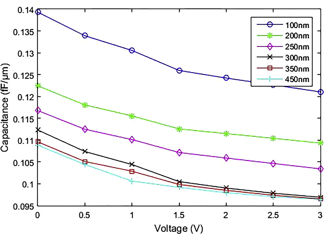
Capacitance vs Voltage for various W i.
The electro-optic effect occurs due to the variation in the carrier concentration. Due to the depletion of carriers present in the waveguide by the application of V, the effective index
where, n eff,i = effective index of the waveguide without doping
Change in the effective index (Figure 6) causes the change in phase (Figure 7) of the light being transmitted in the arm of the modulator (L). From Figure 7 it is inferred that an increase in W i reduces the number of carriers needed for effective index change to produce the necessary phase shift, thus reducing the phase shift. From Figure 8 it is inferred that as the exposure of the dopants to the photons is minimized, the loss is reduced.

Effective index vs Voltage for W i.

Phase shift vs Voltage for various W i.

Loss vs Voltage for varying W i.
With further increase in voltage, the carriers are depleted from the waveguide reducing the optical carrier absorption loss. The phase shifter is used in an arm of the unbalanced MZM with an arm length difference of 100 µm. The transmission per wavelength for voltage (V) is calculated using equation (5).
The transmission spectra lie within λ = 1553.4–1553.7 nm and the wavelength 1553.5 nm is selected for detailed study. In order to study the W i variations in the modelled PIN structure, the analysis was performed at 20 Gbps with NRZ technique for Pseudo-Random Bit sequence. A phase shift of 180° is required to obtain the modulation and extinction ratio is calculated from the obtained eye diagram. When the W i is small, the carrier absorption loss occurs leading to a reduction in BER and the increase in W i improves the BER but requires high voltage to produce the required phase shift. Higher extinction ratio with good BER (Table 1) was obtained for W i = 100 and 250 nm at 1 and 2 V respectively for 5 mm phase shifter.
Comparison of ER and BER for PS length = 5 mm with intrinsic gap, W 2 = 250 nm & W 1 = 100 nm.
| V | W 2 | W 1 | ||
|---|---|---|---|---|
| ER (dB) | BER | ER (dB) | BER | |
| 0.5 | 2.95 | 1.40 × 10−04 | 6.67 | 1.62 × 10−07 |
| 1 | 6.41 | 1.45 × 10−08 | 24.08 | 3.32 × 10⁻¹² |
| 2 | 21.42 | 2.48 × 10⁻¹⁴ | 16.89 | 1.39 × 10−03 |
| 3 | 9.63 | 1.79 × 10⁻¹¹ | 3.50 | 2.43 × 10−08 |
When the PS length is reduced to 2 mm, the reduction in dopant exposure length decreases the optical loss leading to good BER at the expense of the ER (Table 2). In order to get a high ER, the intrinsic region has to be near the high-intensity optical centre and also high voltage is required, as the exposure length is less. For W 2 & PS length = 2 mm, voltage >3 V is required for obtaining high ER with acceptable BER. From Table 2, it is observed that the effective index change to produce the destructive interference occurred at 3 V for 2 mm PS length to obtain 23.707 dB ER and 3.522 × 10⁻¹⁴ BER at 20 Gbps.
Comparison of ER and BER for PS length = 2 mm W 2 & W 1.
| V | W 2 | W 1 | ||
|---|---|---|---|---|
| ER (dB) | BER | ER (dB) | BER | |
| 0.5 | 1.07 | 1.52 × 10−02 | 2.05 | 4.55 × 10−03 |
| 1 | 2.05 | 1.49 × 10−03 | 4.39 | 2.69 × 10−06 |
| 2 | 4.04 | 1.46 × 10−06 | 10.69 | 8.27 × 10⁻¹² |
| 3 | 6.38 | 1.80 × 10−09 | 23.70 | 3.52 × 10⁻¹⁴ |
With wider eye-opening and lower jitter, high-speed transmission for the modulator is possible. The eye-crossing lies above 23% (Figure 9) in the zero signal level which causes the timing for ‘one’ pulse to be lower than that of ‘zero’ pulse at higher bitrate with the alternating 0’s and 1’s. The timing for one pulse further reduces which degrades the BER. The eye being wider with sharp rise and fall times, reduces the Duty Cycle Distortion (DCD) which measures the time distortions for the signals one and zero. DCD is given by equation (6).

Eye diagram at 20 Gbps (a) PS = 5 mm with W 2 at 2 V, (b) PS = 5 mm with W 1 at 1 V, (c) PS = 2 mm with W 1 at 3 V.
The deviation from the ideal 0% of DCD leads to error in reception causing an increase in BER. DCD is calculated to be ∼3% for Figure 9, which makes the modulator feasible for higher transmission rates. Carrier concentration variation [A = (P = 7 × 1018 cm−3 & N = 5 × 1018 cm−3), B = (P = 7 × 1017 cm−3 & N = 5 × 1017 cm−3) and C = (P = 7 × 1018 cm−3 & N = 5 × 1018 cm−3)] is analysed for PS length 5 & 2 mm. When the carrier concentration is increased, the carriers that are not near the junction remain un-depleted which results in the decrease of modulator efficiency due to the increase in loss. The decrease of the carrier concentration reduces the absorption loss but also minimizes the eye-opening leading to a reduction in ER and an increase in required voltage. For W2 and PS length = 5 mm (L) in P & N = 1018 cm−3, the DCD value increased causing the BER to increase. Thus from the tabulated results (Table 3), it is clear that for the designed structure, 1017 cm−3 carrier concentration provides better ER and BER for optical communication.
Carrier concentration variation comparison at 20 Gbps.
| Conc. | V | ER (dB) | BER | α (dB/ cm) | V π L π (Vcm) |
|---|---|---|---|---|---|
| A-W 1 | 1 | 22 | 3.6 × 10⁻¹¹ | 3.47 | 0.5 |
| A-W 1 | 3 | 21.9 | 2.3 × 10⁻¹³ | 3.05 | 0.6 |
| A-W 2 | 0.5 | 20.9 | 4.2 × 10−06 | 2.24 | 0.25 |
| B-W 1 | 1 | 24 | 3.3 × 10⁻¹² | 2.82 | 0.5 |
| B-W 1 | 3 | 23.7 | 3.5 × 10⁻¹⁴ | 2.42 | 0.6 |
| B-W 2 | 2 | 21.4 | 2.5 × 10⁻¹⁴ | 1.94 | 1 |
| C-W 1 | 3 | 17.2 | 4.2 × 10⁻²⁰ | 0.03 | 1.5 |
The timing for one pulse being lower than that of zero pulse causes an increase in BER at high speeds. When the Bit rate is increased to 50 Gbps, it is observed (Table 4) that PS length = 5 mm with W2, (V π L π = 1 Vcm) produces acceptable BER with good ER. For W 1, an increase in exposure of dopants to light raises the optical loss and with DCD further deviating from zero causes a decrease in BER, making the device unsuitable for high-speed applications.
W 1 & W 2 comparison for higher data rate (Gbps) for P = 7 × 1017 cm−3 & N = 5 × 1017 cm−3.
| W i | L (mm) | Gbps | V | ER (dB) | BER |
|---|---|---|---|---|---|
| W 1 | 5 | 20 | 1 | 24.08 | 3.32 × 10⁻¹² |
| 50 | 23.84 | 8.66 × 10−08 | |||
| 100 | 22.32 | 6.16 × 10−05 | |||
| 2 | 20 | 3 | 23.70 | 3.52 × 10⁻¹⁴ | |
| 50 | 23.41 | 1.00 × 10−07 | |||
| 100 | 21.59 | 2.05 × 10−05 | |||
| W 2 | 5 | 20 | 2 | 21.42 | 2.48 × 10⁻¹⁴ |
| 50 | 21.19 | 8.98 × 10−08 | |||
| 100 | 20.65 | 2.70 × 10−05 |
Various doping patterns were experimented in order to obtain high modulation efficiency. Few of the recently published articles are compared in Table 5.
Proposed work I: When W i = 100 nm & PS length = 5 mm, 0.5 V π L π is achieved. The loss affects the BER which is due to the high dopant exposure. To reduce the loss, the length of the phase shifter was reduced to 2 mm (W i = 100 nm) resulted in increase of V π L π to 0.6 Vcm and loss 2.42753 dB/cm.
Proposed work II: At W i = 250 nm & PS length = 5 mm, the loss is minimised (1.94663 dB/cm) due to the reduction in dopant exposure to the light at the expense of 1 Vcm V π L π.
The above results demonstrate that the proposed design outperforms the other devices.
The proposed modulator with 2 mm phase shifter was analysed for intra data centre communication till 15 km in Lumerical Interconnect. The simulation setup is explained in Figure 10. The analysis was performed for a bit rate of 100 Gbps and laser beam of 1553.5 nm wavelength. The pre optical amplifier setup was used with the amplifier gain of 20 dB. The optical fibre has a dispersion of 16 ps/nm/km and attenuation of 0.2 dB/km. BER and ER was measured as the length of the optical fibre was varied (Table 6). It is observed that the BER obtained is well below the FEC threshold level of 3.8 × 10⁻³.
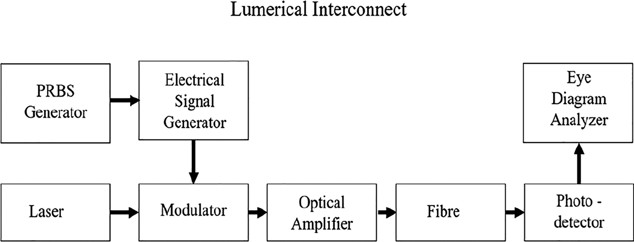
Process flow for intra data centre communication analysis.
Parameter comparison.
| Ref | λ (nm) | Gbps | L (mm) | V π L π (Vcm) |
|---|---|---|---|---|
| [11] | 1550 | 25 | ∼1 | 0.76 |
| [10] | 1549.4 | 10 | 6 | 7.2 |
| [9] | 1550 | >25 | 1.8 | 0.72 |
| [12] | ∼1550 | 28 | 3 | 0.8–1.86 |
| [13] | 1310 | 24 | 2 | 0.46 |
| [14] | ∼1576 | 40 | 2 | 1.8 |
| [15] | ∼1550 | 56 & 100 | 5 | 2.5 |
| Proposed work I | 1553.5 | 100 | 2 | 0.6 |
| Proposed work II | 1553.5 | 100 | 5 | 1 |
Intra data centre communication at 100 Gbps.
| Length (Km) | Voltage (V) | ER (dB) | BER |
|---|---|---|---|
| 10 | 3 | 16.96 | 1.42 × 10−05 |
| 15 | 3 | 11.05 | 4.97 × 10−03 |
As the length increased due to dispersion and attenuation present in the fibre the ER decreased and BER increased. From the analysis it is found that the proposed modulator is suited for inter and intra chip communication.
4 Conclusion
In this paper high-performance Carrier depletion Silicon PIN phase shifter is designed and numerical analysis was performed for the range of 100–450 nm intrinsic gaps for PS length of 2 and 5 mm. The optimum intrinsic gap with dopant concentration for rib waveguide structure is designed and analysed considering the trade-off condition between the ER, BER and loss for obtaining high modulation efficiency at minimum voltage. The designed phase shifter in MZM has 24.088 & 23.707 dB ER at 20 Gbps for 5 & 2 mm lengths at 1 V and 3 V respectively. For 100 Gbps and PS lengths 5 and 2 mm, 22.32 & 21.59 dB ER is obtained at 1 V & 3 V respectively. An optimum intrinsic gap i.e. 250 in 5 mm PIN phase shifter was found to produce 21.19 dB ER with BER 8.98 × 10⁻⁸ and dB 20.65 ER with BER 2.70 × 10−05 at 2 V, for 50 and 100 Gbps respectively having V π L π as 1 Vcm. The proposed design was also analysed in an intra-data centre communication setup of fibre length 15 km. This paper reports an optimum value of intrinsic gap and dopant concentration to obtain high modulation efficiency and speed, for PIN phase shifter at low voltage.
Acknowledgments
Authors would like to thank Vellore Institute of Technology (VIT), Chennai, India for providing the resources and support for this work.
-
Author contribution: All the authors have accepted responsibility for the entire content of this submitted manuscript and approved submission.
-
Research funding: None declared.
-
Conflict of interest statement: The authors declare no conflicts of interest regarding this article.
References
1. Tu, X, Liow, TY, Song, J, Luo, X, Fang, Q, Yu, M, et al. 50-Gb/s silicon optical modulator with traveling-wave electrodes. Opt Express 2013;21:12776–82. https://doi.org/10.1364/oe.21.012776.Search in Google Scholar PubMed
2. Reed, GT, Mashanovich, GZ, Gardes, FY, Nedeljkovic, M, Hu, Y, Thomson, DJ, et al. Recent breakthroughs in carrier depletion based silicon optical modulators. Nanophotonics 2014;3:229–45. https://doi.org/10.1515/nanoph-2013-0016.Search in Google Scholar
3. Soref, RI, Bennett, BR. Electrooptical effects in silicon. IEEE J Quant Electron 1987;23:123–9. https://doi.org/10.1109/jqe.1987.1073206.Search in Google Scholar
4. Tanaka, S, Simoyama, T, Aoki, T, Mori, T, Sekiguchi, S, Jeong, SH, et al. Ultralow-power (1.59 mW/Gbps), 56-Gbps PAM4 operation of Si photonic transmitter integrating segmented PIN Mach–Zehnder modulator and 28-nm CMOS driver. J Lightwave Technol 2018;36:1275–80. https://doi.org/10.1109/jlt.2018.2799965.Search in Google Scholar
5. Azadeh, SS, Müller, J, Merget, F, Romero-García, S, Shen, B, Witzens, J. Advances in silicon photonics segmented electrode Mach-Zehnder modulators and peaking enhanced resonant devices. In: Photonics North 2014. International Society for Optics and Photonics; 2014, vol 9288:928817 p.Search in Google Scholar
6. Xu, H, Xiao, X, Li, X, Hu, Y, Li, Z, Chu, T, et al. High speed silicon Mach-Zehnder modulator based on interleaved PN junctions. Opt Express 2012;20:15093–9. https://doi.org/10.1364/oe.20.015093.Search in Google Scholar PubMed
7. Xu, H, Li, X, Xiao, X, Li, Z, Yu, Y, Yu, J. Demonstration and characterization of high-speed silicon depletion-mode Mach–Zehnder modulators. IEEE J Sel Top Quant Electron 2013;20:23–32. https://doi.org/10.1109/JSTQE.2013.2293763.Search in Google Scholar
8. Yu, H, Pantouvaki, M, Van Campenhout, J, Korn, D, Komorowska, K, Dumon, P, et al. Performance tradeoff between lateral and interdigitated doping patterns for high speed carrier-depletion based silicon modulators. Opt Express 2012;20:12926–38. https://doi.org/10.1364/oe.20.012926.Search in Google Scholar PubMed
9. Azadeh, SS, Merget, F, Romero-García, S, Moscoso-Mártir, A, von den Driesch, N, Müller, J, et al. Low V π Silicon photonics modulators with highly linear epitaxially grown phase shifters. Opt Express 2015;23:23526–50. https://doi.org/10.1364/oe.23.023526.Search in Google Scholar PubMed
10. Goi, K, Ogawa, K, Tan, YT, Dixit, V, Lim, ST, Png, CE, et al. Silicon Mach-Zehnder modulator using low-loss phase shifter with bottom PN junction formed by restricted-depth doping. IEICE Electron Express 2013;10:20130552. https://doi.org/10.1587/elex.10.20130552.Search in Google Scholar
11. Rosenberg, JC, Green, WM, Assefa, S, Gill, DM, Barwicz, T, Yang, M, et al. A 25 Gbps silicon microring modulator based on an interleaved junction. Opt Express 2012;20:26411–23. https://doi.org/10.1364/oe.20.026411.Search in Google Scholar
12. Maegami, Y, Cong, G, Ohno, M, Okano, M, Itoh, K, Nishiyama, N, et al. High-efficiency strip-loaded waveguide based silicon Mach-Zehnder modulator with vertical pn junction phase shifter. Opt Express 2017;25:31407–16. https://doi.org/10.1364/oe.25.031407.Search in Google Scholar PubMed
13. Yong, Z, Sacher, WD, Huang, Y, Mikkelsen, JC, Yang, Y, Luo, X, et al. Efficient single-drive push-pull silicon Mach-Zehnder modulators with U-shaped PN junctions for the O-band. In: Optical fiber communication conference. Optical Society of America; 2017:Tu2H-2 pp.10.1364/OFC.2017.Tu2H.2Search in Google Scholar
14. Wang, C, Zhang, M, Stern, B, Lipson, M, Lončar, M. Nanophotonic lithium niobate electro-optic modulators. Opt Express 2018;26:1547–55. https://doi.org/10.1364/oe.26.001547.Search in Google Scholar PubMed
15. He, M, Xu, M, Ren, Y, Jian, J, Ruan, Z, Xu, Y, et al. High-performance hybrid silicon and lithium niobate Mach–Zehnder modulators for 100 Gbit s− 1 and beyond. Nat Photon 2019;13:359. https://doi.org/10.1038/s41566-019-0378-6.Search in Google Scholar
16. Chrostowski, L, Hochberg, M. Silicon photonics design: from devices to systems. Cambridge University Press; 2016:217–23 pp.10.1017/CBO9781316084168Search in Google Scholar
© 2020 Jesuwanth Sugesh Ramesh Gabriel and Sivasubramanian Arunagiri, published by De Gruyter, Berlin/Boston
This work is licensed under the Creative Commons Attribution 4.0 International License.
Articles in the same Issue
- Frontmatter
- Amplifiers
- Editorial
- Erbium/Ytterbium-Doped Waveguide Amplifier (EYDWA) for extended reach of Wavelength Division Multiplexing based free space optics system (WDM/FSO)
- The effect of doping on the electrons and holes in quantum dot semiconductor optical amplifiers
- Performance analysis and parameter optimization of all-optical encryption using the FWM effect in semiconductor optical amplifier
- Total gain of InTlAsSb quantum dot structures
- Gain-forming effect on optical signal-to-noise ratio in Raman fiber amplifier
- Design of EDFA based 16 channel WDM system using counter directional high pump power
- Polarization rotation-based all-optical AND gate using single semiconductor optical amplifier and implementation of a majority gate
- Performance analysis on double-pass thulium-doped fiber amplifier for 16-channel WDM system at S-band
- Design of optical packet switch in presence of dispersion compensation and amplifier noise
- Alternative method of implementation of all-optical NOR and NAND gates using quantum-dot semiconductor optical amplifiers in non-interferometer structure
- Detectors
- A long-reach radio over free space optics (Ro-FSO) system using hybrid orthogonal frequency division multiplexing (OFDM)-multibeam concept with enhanced detection
- BER performance analysis of FSO using hybrid-SIM technique with APD receiver over weak and strong turbulence channels
- High-speed and long-reach PON employing PM-DQPSK signal and coherent receiver
- Devices
- Multi-Layer Graded-Index Planar Structure for Coarse WDM Demultiplexing
- Photonic Crystal-Based All-Optical Half Adder with High Contrast Ratio
- Distributed Feedback Laser (DFB) for Signal Power Amplitude Level Improvement in Long Spectral Band
- Performance analysis of carrier depletion silicon PIN phase shifter
- Design of Optical 4 × 2 Encoder Using Cross Layered Chalcogenide2D-PC Resonator
- 1 × 2 plasmonic wavelength demultiplexer using rectangular MIM waveguide
- Compact and efficient PC-based directional coupler all-optical switch
- All-optical integrated 2-to-4 decoder and 1-to-4 demultiplexer circuit with enable using SOA based MZI
- All optical half subtractor based on threshold switching and beams interference mechanisms
- An All Optical Photonic Crystal Based XOR Gate for BPSK Signals
- Four bits data sequence generators based ytterbium doped fiber amplifiers for upgrading maximum Q factor and minimum BER
- Design and optimization of all-optical demultiplexer using photonic crystals for optical computing applications
- Hybrid buffer‐based optical packet switch with negative acknowledgment for multilevel data centers
- Application of photonic crystal based nonlinear ring resonators for realizing all optical 3-to-8 decoder
- Power conversion with complete photonic band gap in magneto-photonic crystal slab based on cerium-substituted yttrium iron garnet
- Performance comparison of all-optical logic gates using electro-optic effect in MZI-based waveguide switch at 1.46 µm
- Modelling and analysis of chirped long-period grating inscribed in a planer optical waveguide structure for sensing applications
- Comparative study of all-optical INVERTER and BUFFER gates using MZI structure
- Design of multiplexing circuit using electro-optic effect based optical waveguides
- Performance enhancement of ultra-dense WDM over FSO hybrid optical link by incorporating MIMO technique
- A novel proposal based on 2D linear resonant cavity photonic crystals for all-optical NOT, XOR and XNOR logic gates
- All optical NAND/NOR and majority gates using nonlinear photonic crystal ring resonator
- Proposed model of all optical reversible and irreversible modules on a single photonic circuit
- A photonic crystal based de-multiplexer with uniform channel spacing
- An all optical photonic crystal half adder suitable for optical processing applications
- Modelling of symmetrical quadrature optical ring resonator with four different topologies and performance analysis using machine learning approach
- Effect of misalignment on coupling efficiency in laser diode to single-mode circular core graded-index fiber coupling via cylindrical microlens on the fiber tip
- A critical review of optical switches
- An ultra-dense spacing-based PON by incorporating dual drive Mach–Zehnder modulator for comb generation
- Logic gates based on optical transistors
- Compact and ultrafast all optical 1-bit comparator based on wave interference and threshold switching methods
- A high speed all optical half adder using photonic crystal based nonlinear ring resonators
- Ultrafast all optical XOR gate using photonic crystal-based nonlinear ring resonators
- Investigating the performance of all-optical AND logic gate based on FWM effect in SOA at low power
- Nonlinear optical decoder based on photonic quasi crystal ring resonator structure
- Optical data center switches design and analysis
- Hybrid buffer and AWG based add-drop optical packet switch
- Solitons based optical packet switch analysis
- A photonic transmission link with enhanced dynamic range by incorporating phase shifters in dual drive dual parallel Mach–Zehnder modulator
- Using nonlinear ring resonators for designing an all optical comparator
- All optical half subtractor based on linear photonic crystals and phase shift keying technique
- Multi-input single-output (MISO) all optical logic (ALG) AND/NOR gate using FWM in dispersion compensation fibers in Mach-Zehnder configuration (DCF-MZI)
- Wavelength and throughput tuning of FORR-based optical filter using Sagnac effect
- Performance Enhancement of Encoding–Decoding Multidiagonal and Walsh Hadamard Codes for Spectral Amplitude Coding-Optical Code Division Multiple Access (SAC-OCDMA) Utilizing Dispersion Compensated Fiber
- Impact Analysis of the Number of Core on Hexagonal Multicore Fibre
- Effect of OPC on Fiber Nonlinearities for Dense Soliton Optical Communication Medium
- Sensing of Illegal Drugs by Using Photonic Crystal Fiber in Terahertz Regime
- On characteristic behavior and flattened chromatic dispersion properties of bent photonic crystal fibers
- Ultra high birefringent dispersion flattened fiber in terahertz regime
- Structural dependence of transmission characteristics for photonic crystal fiber with circularly distributed air-holes
- Numerical analysis of photonic crystal fibre with high birefringence and high nonlinearity
- Exploiting higher-order mode dispersion of bend M-type chalcogenide fiber in mid-IR supercontinuum generation
- Design of optoelectronic oscillator based on multiple-length single mode fiber and chirped fiber Bragg grating
- Modulation instability in nonlinear chiral fiber
- High birefringence and broadband dispersion compensation photonic crystal fiber
- Design and analysis of highly nonlinear, low dispersion AlGaAs-based photonic crystal fiber
- Highly negative dispersion compensating fiber with low third order dispersion
- Dispersion properties of single-mode optical fibers in telecommunication region: poly (methyl methacrylate) (PMMA) versus silica
- Influence of Kerr nonlinearity on group delay and modal dispersion parameters of single-mode graded index fibers: evaluation by a simple but accurate method
- Highly birefringent photonic crystal fiber with D-shaped air holes for terahertz (THz) application
- Simulation and analysis of ultra-low material loss of single-mode photonic crystal fiber in terahertz (THz) spectrum for communication applications
- Investigation of radiation induced luminescence with modulated signal transmission in optical fiber
- Design and analysis of uncoupled heterogeneous trench-assisted multi-core fiber (MCF)
- Simulative study of raised cosine impulse function with Hamming grating profile based Chirp Bragg grating fiber
- Highly Efficient Solar Energy Conversion Using Graded-index Metamaterial Nanostructured Waveguide
- Chaotic Synchronization of Mutually Coupled Lasers with Another Laser and Its Encoding Application in Secret Communication
- Passively Femtosecond Mode-Locked Erbium-Doped Fiber Oscillator with External Pulse Compressor for Frequency Comb Generation
- Conventional band demultiplexer with high quality factor and transmission power based on four optimized shaped photonic crystal resonators
- Different modulation schemes for direct and external modulators based on various laser sources
- Third order intermodulation and third order intercept in a directly modulated Fabry–Perot laser diode
- Evaluation of quantum dot light-emitting diodes synchronization under optically feedback
- Laser diode to single-mode graded index fiber coupling via cylindrical microlens on the fiber tip: evaluation of coupling efficiency by ABCD matrix formalism
- Enhanced Performance Analysis of 10 Gbit/s–10 GHz OFDM-Based Radio over FSO Transmission System Incorporating ODSB and OSSB Modulation Schemes
- An Ultra-compact Plasmonic Modulator Using Elasto-optic Effect and Resonance Phenomena
- Performance Comparison of Free-Space Optical (FSO) Communication Link Under OOK, BPSK, DPSK, QPSK and 8-PSK Modulation Formats in the Presence of Strong Atmospheric Turbulence
- Model for Performance Improvement of Blocking Probability in GMPLS Networks
- Study on P2P Service Bearer Method for Passive Optical Network for Long Distance and Wide Access
- Physical layer impairment-aware ant colony optimization approach in WDM network
- Analysis of Laser Linewidth on the Performance of Direct Detection OFDM Based Backhaul and Backbone Networks
- Radio over fiber based signal transport schemes for emerging mobile fronthaul networks – a review
- A Comparative Study of Performances Between the WDM PON System and the CWDM PON System in an Optical Access Network
- Beam divergence and operating wavelength bands effects on free space optics communication channels in local access networks
- Proactive link handover deploying coordinated transmission for indoor visible light communications (VLC) networks
- Optimized Dynamic Bandwidth Allocation Algorithm for Optical Access Networks
- Packet Blocking Performance of Cloud Computing Based Optical Data Centers Networks under Contention Resolution Mechanisms
- Optimization of an EYDWA Amplifier Parameters for a Gigabit Passive Optical Network (GPON)
- Research on Power Optimization Based on Adaptive Passive Optical Networks
- Towards cloud transport using IP-multiservices access network (MSAN)
- Enhanced redirection strategy for peer to peer services in high-speed and large-capacity ethernet passive optical networks
- Transmission challenges in metropolitan area optical networks
- Performance evaluation of a multihop WDM network with share-per-node L-WIXC architecture
- Performance analysis of hybrid optical amplifiers for multichannel wavelength division multiplexed (WDM) optical networks
- Time-domain Measurement and Analysis of Differential Mode Delay and Modal Bandwidth of Graded-Index Multimode Fiber in SDM Networks
- Seven-channel 1 Gbps TWDM coexistence architecture supporting 65 Gbps optical link for next-generation passive optical network 2–based FTTX access networks
- Link failure recovery using p-cycles in wavelength division multiplex (WDM) mesh networks
- Cascadability analysis of WDM recirculating loop buffer-based switch in optical data networks
- Evolution of optical networks: from legacy networks to next-generation networks
- A novel framework for content connectivity through optical data centers
- Performance of different hybrid dispersion compensation modules (DCMs) in long reach ultra dense WDM passive optical networks
- Performance investigation of PM-based wavelength remodulation scheme in bidirectional TWDM-PON
- Physical layer analysis of optical wireless data centers
- Novel approach to jointly optimize working and spare capacity of survivable optical networks
- A QoS provisioning architecture of fiber wireless network based on XGPON and IEEE 802.11ac
- Radio over fiber on gigabit passive optical network using QPSK modulation scheme
- Blocking performance of optically switched data networks
- Devices, communication techniques and networks for all optical communication: research issues
- Design and investigation of N1-class next-generation passive optical network-2 (NG-PON2) coexistence architecture in the presence of Kerr effect and four-wave mixing (FWM) for fiber to the home (FTTX) access networks
- Improved algorithm for enhance robustness of IPTV based on GEPON
- Simultaneous distribution of wired and two 2 × 2 MIMO wireless OFDM signals over an integrated RoF-PON system
- Analyzing optical TDMA to mitigate interference in downlink LiFi optical attocell networks
- Light fidelity optical network a comparative performance evaluation
- Theory of chaos synchronization and quasi-period synchronization of an all optic 2n-D LAN
- Performance of high scalability hybrid system of 10G-TDM-OCDMA-PON based on 2D-SWZCC code
- Performance analysis of APD and PIN diode with and without EDFA in GPON
- Improved Performance Investigation of 10 Gb/s–10 GHz 4-QAM Based OFDM-Ro-FSO Transmission Link
- Feasibility Analysis of Optical Wireless Communication for Indian Tropical and Subtropical Climates
- 40 Gb/s High-speed mode-division multiplexing transmission employing NRZ modulation format
- Performance Analysis of Shift ZCC Codes and Multi Diagonal Codes in 100 Gbps MDM-FSO System
- Combined Envelope Scaling with Modified SLM Method for PAPR Reduction in OFDM-Based VLC Systems
- Empirical Evaluation of High-speed Cost-effective Ro-FSO System by Incorporating OCDMA-PDM Scheme under the Presence of Fog
- Satellite-to-Ground FSO System Based on Multiaperture Receivers as an Optimization Solution for Strong Turbulence and Fog Conditions
- Performance analysis of NRZ and RZ variants for FSO communication system under different weather conditions
- Free space optics communication system design using iterative optimization
- Optical wireless systems with ASK & PSK using coupler-based delay line filter
- Probing of nonlinear impairments in long range optical transmission systems
- Design and Investigation of Free Space Optical System for Diverse Atmospheric Transmission Windows
- The performance comparison of hybrid WDM/TDM, TDM and WDM PONs with 128 ONUs
- Performance evaluation of a multiple optical link FSO–FSO
- Analysis the flat gain/noise figure using RAMAN-Reflective Semiconductor Hybrid Optical Amplifier in C + L + U triple band for super dense wavelength division multiplexing system
- Design improvement to reduce noise effect in CDMA multiple access optical systems based on new (2-D) code using spectral/spatial half-matrix technique
- High-speed signal processing and wide band optical semiconductor amplifier in the optical communication systems
- 2 × 20 Gbit/s OFDM-based FSO transmission system for HAP-to-ground links incorporating mode division multiplexing with enhanced detection
- Radio-over-fiber front-haul link design using optisystem
- A 2 × 20 Gbps hybrid MDM-OFDM–based high-altitude platform-to-satellite FSO transmission system
- Analysis of hybrid integrated-alternate mark inversion (I-AMI) modulation and symmetrical-symmetrical-post (SSP) dispersion compensation technique in single-tone radio over fiber (RoF) system
- Peak to average power ratio (PAPR) reduction in filter bank multicarrier (FBMC) and orthogonal frequency division multicarrier (OFDM) based visible light communication systems
- Development and performance improvement of a novel zero cross-correlation code for SAC-OCDMA systems
- Comparative analysis of SISO and wavelength diversity-based FSO systems at different transmitter power levels
- Effect of adverse weather conditions and pointing error on the performance of 2-D WH/TS OCDMA over FSO link
- Performance of LED for line-of-sight (LoS) underwater wireless optical communication system
- Underwater wireless optical communication: a case study of chlorophyll effect
- Subcarrier multiplexed radio over fiber system with optical single sideband modulation
- Performance investigation of free space optics link employing polarization division multiplexing and coherent detection-orthogonal frequency division multiplexing under different link parameters
- Performance analysis of FSO link under the effect of fog in Delhi region, India
- Design and analysis of full duplex RoF system with efficient phase noise cancellation from a coherent RoF system
- Mathematical modeling of optical impairments in DSP based WDM coherent system
- Analysis of 64 channels based IS-OWC system using different intereference reduction techniques
- Effects of local oscillator on the performance of DP-QPSK WDM system with channel spacing of 37.5 GHz
- Dual band radio-over-fibre millimetre–wave system utilizing optical frequency combs
- Full duplex dispersion compensating system based on chromatic dispersion in analog RoF links
- Performance enhancement of Raman + EYDFA HOA for UD-WDM system applications
- Crosstalk characterization in homogeneous multicore fiber using discrete changes model under bidirectional propagation
- Analysis three dispersion compensation techniques using DCF
- Electrocardiogram transmission over OFDM system
- A multilayers adaptive ALACO-OFDM for spectral efficiency improvement using PSO algorithm in visible light communication systems
- A comprehensive road map of modern communication through free-space optics
- Performance of orthogonal frequency division multiplexing based 60-GHz transmission over turbulent free-space optical link
- Design of 16 × 40 Gbps hybrid PDM-WDM FSO communication system and its performance comparison with the traditional model under diverse weather conditions of Bangladesh
- Next generation optical wireless communication: a comprehensive review
- A companding approach for PAPR suppression in OFDM based massive MIMO system
- Characterization of terrestrial FSO link performance for 850 and 1310 nm transmission wavelengths
- Analysis of nonlinear behavior of multimode spatial laser beams with high stability and coherence for medical applications
- Performance of a free space optical link employing DCO-OFDM modulated Gaussian-beam
- Nonlinear/dispersion compensation in dual polarization 128-QAM system incorporating optical backpropagation
- New encoding/decoding design of SAC-OCDMA system with fixed correlation zone code
- Theoretical investigation of multiple input–multiple output (MIMO) technique for line of sight (LoS) underwater wireless optical communications system
- Dimming controlled multi header pulse position modulation (MH-PPM) for visible light communication system
- 40 Gb/s wavelength division multiplexing-passive optical network (WDM-PON) for undersea wireless optical communication
- Analyzing of UVLC system considering the effect of water depth
- On the transmission of data packets through fiber-optic cables of uniform index
- Performance analysis of WDM free space optics transmission system using MIMO technique under various atmospheric conditions
- Review on nonlinearity effect in radio over fiber system and its mitigation
- Improving the optical link for UVLC using MIMO technique
- A review on signal generation techniques in radio over fiber systems
- FBMC OQAM: novel variant of OFDM
- A 120 Mbps WDM-based VLC system for implementation of Internet of Things
- Physical layer security analysis of a dual-hop hybrid RF-VLC system
- Application scheme and performance analysis of free space optical communication technology in INMARSAT
- Artificial intelligence based optical performance monitoring
- Mobility aware of WDM-based CMO OFDM communication system
- Design and performance analysis of spectral-efficient hybrid CPDM-CO-OFDM FSO communication system under diverse weather conditions
- An approach to ensure joint illumination & communication performance of a forward error corrected indoor visible light communication (VLC) system in presence of ambient light interference
- A Large-Capacity Optical Switch Design for High-Speed Optical Data Centers
- Performance Analysis of OWC Using NOP Technique
- Performance Evaluation of a Hybrid Buffer-Based Optical Packet Switch Router
- Modeling C2 n by Inclusion of Rainfall Parameter and Validate Modified Log Normal and Gamma-Gamma Model on FSO Communication Link
- Enhancement of reliability and security in spatial diversity FSO-CDMA wiretap channel
- FSO-Based Analysis of LTE-A MAC Protocols to Achieve Improved QoS
- Dynamic routing and wavelength assignment for efficient traffic grooming
- High Birefringence and Negative Dispersion Based Modified Decagonal Photonic Crystal Fibers: A Numerical Study
- Impact of Pointing Error on the BER Performance of an OFDM Optical Wireless Communication Link over Turbulent Condition
- A receiver intensity for Super Lorentz Gaussian beam (SLG) propagation via the moderate turbulent atmosphere using a novelty mathematical model
- Performances of BICM-ID system using CRSC code in optical transmissions
- 128-QAM dual-polarization chaotic long-haul system performance evaluation
- Suppression of nonlinear noise in a high-speed optical channel with variable dispersion compensation
- Radio over fiber (RoF) link modelling using cross term memory polynomial
- An investigation of 16-QAM signal transmission over turbulent RoFSO link modeled by gamma–gamma distribution
- Design of 320 Gbps hybrid AMI-PDM-WDM FSO link and its performance comparison with traditional models under diverse weather conditions
- Non-linear companding scheme for peak-to-average power ratio (PAPR) reduction in generalized frequency division multiplexing
- Implementation of wavelet transform based non-Hermitian symmetry OFDM for indoor VLC system using Raspberry Pi
- PAPR reduction scheme for optical OFDM techniques
- Investigations with all optical sequential circuit at higher data rate
- Error performance analysis of optical communication over Lognormal-Rician turbulence channel using Gram-Charlier Series
- A simple but accurate method for prediction of splice loss in mono-mode dispersion shifted and dispersion flattened fibers in presence of Kerr nonlinearity
- Simulation modeling of free space optical communication system
- Digital predistortion of radio over fiber (RoF) link using hybrid Memetic algorithm
- Design of a low cost and power efficient 200/400 Gbps optical interconnect using DAC-less simplified PAM4 architecture
- Evaluation of inter-aircraft optical wireless communication system with different modulation formats
- Performance analysis of DP-MZM radio over fiber links against fiber impairments