Reconfigurable frequency selective surface based absorber realized using interlocking blocks
-
Gaurav Chaitanya
 ,
Pratik Chawda
,
Pratik Chawda

Abstract
A reconfigurable frequency selective surface (FSS) based absorber structure has been designed using a novel, cost-effective, simple to operate and easy to fabricate 3D printed interlocking blocks. Four different topologies have been investigated and validated through simulation and experimental studies. The basic geometry comprises a 3D printed mounting board, on which different blocks can be attached using interlocking studs. The frequency reconfigurability has been obtained by mechanically changing various resonating blocks on the board, which results in four distinct absorption frequencies at 4.89 GHz, 4.02 GHz, 2.92 GHz and 2.25 GHz achieving the absorptivities of 98.92 %, 96.52 %, 99.3 % and 99.5 % respectively in S and C bands. The absorption characteristics are further justified by evaluating the surface current distribution and impedance responses. The prototypes have been fabricated and tested, and they have attained a good agreement with the simulated responses. The absorption characteristics and operational frequencies remain the same, for all four cases during variations in the polarization angle for oblique incidence for both TE and TM polarizations up to 45°, as studied in the simulation. These have been experimentally verified up to 30° for TE polarization, thereby demonstrating the polarization-independent and angularly stable responses.
1 Introduction
Frequency selective surfaces (FSSs) are periodic structures with significant impacts across a wide variety of applications such as filtration [1], absorption [2], reflection [3], polarization [4], transmission [5], etc., spanning the broader range of the electromagnetic spectrum from microwave [6] and millimeter [7] to terahertz [8] and even the optical range [9]. One significant constraint of conventional FSS-based structures is their restricted and fixed frequency responses once they are fabricated. With recent advancements in technology, reconfigurable geometries are now widely employed, leveraging compact spaces and offering multifunctional performance. Researchers have adopted several approaches to realize various types of reconfigurable or tunable FSS absorbers, contributing to the development of intelligent surfaces [10], adaptive screening of undesired transmissions, tunable radomes [11], and other practical applications.
Among these, three techniques – namely electronic, magnetic, and mechanical methods – have been predominantly used in practice. In the electronic reconfigurable method, various passive and active components such as varactors, p-i-n diodes [12], [13], [14], [15], [16], [17], MEMS switches [18], and solid-state devices are employed to achieve multifunctional responses. However, this approach increases the complexity of design and involves the use of biasing networks [19], [20]. Modifying the coupling between resonating structures and incident waves by introducing perturbations in FSS structures, either wholly or partially, has also been utilized to tune absorption responses [21], [22], [23]. Magnetically controlled reconfigurable systems are characterized by their weight, large response times, and unsuitability for outdoor use [24], [25], [26]. Various adaptable materials have been explored; however, graphene faces limitations due to its commercial availability [27]. There exist various types of mechanically reconfigurable geometries. Researchers have modified the unit cell designs by injecting/extracting liquid metals into unit cells [28], [29], rotating a movable inner element inside metallic grids [30], or using rotating shafts to achieve the desired responses [31]. Other similar techniques to achieve reconfigurability typically involve structural alterations such as shifting, folding, or stretching [32], [33], [34]. However, fluids and liquids pose issues related to leakages, while the other techniques often involve motors, springs, or other devices to change the orientation of structures, making them costly and cumbersome to assemble and maintain stability. In [35], [36], an alternative method for designing FSS-based absorbers with frequency hopping/reconfigurability is introduced, using the physical rearrangement of structural units. However, these designs tend to have larger dimensions and thicknesses, resulting in larger footprints.
In this paper, a cheaper, simple-to-design-and-fabricate, reusable, miniaturized, and easy-to-reconfigure approach is introduced for the design of an FSS-based absorber using three-dimensionally (3-D) printed interlocking blocks. The frequency reconfigurability has been obtained by mechanically changing resonating blocks on an interlocking design based mounting board. Four distinct absorption responses have been obtained at 4.89 GHz, 4.02 GHz, 2.92 GHz, and 2.25 GHz with absorptivities of 98.92 %, 96.52 %, 99.3 %, and 99.5 %, respectively, in S and C bands. This method has removed the use of complicated diode-based electronically reconfigurable technique, and offers a dynamic switching of frequencies by simple mechanical replacement of interlocking blocks. While switching the absorption frequency, different resonator patterns are used having similar constituent substrates and periodic dimensions. This has further helped to achieve more compact absorber geometry, by exploiting innovative unit cell topologies. The geometry has been analyzed concerning various polarization angles, incident angles, impedance responses, and surface current distributions, followed by experimental validation using 3-D printing techniques. The results validate the novel aspects of the proposed frequency-reconfigurable FSS absorber.
2 Unit cell design
The presented design comprises two distinct segments: the mounting board with elevated studs, serving as the base, and block mounts with conductive patterns on their tops. These block mounts are fabricated in various shapes corresponding to different resonating structures, featuring interlocking patterns on their bottoms. This allows them to be easily replaced to achieve reconfigurable responses. Importantly, this replacement process does not require significant mechanical alterations or the integration of additional components, making the technique efficient. Four resonating element topologies have been considered: cross dipole, square loop, cross dipole with increased arm length, and swastika, as depicted in Figure 1. Their dimensions are chosen such that their absorption frequencies are distinct and fall within the S (2–4 GHz) and C (4–8 GHz) bands.
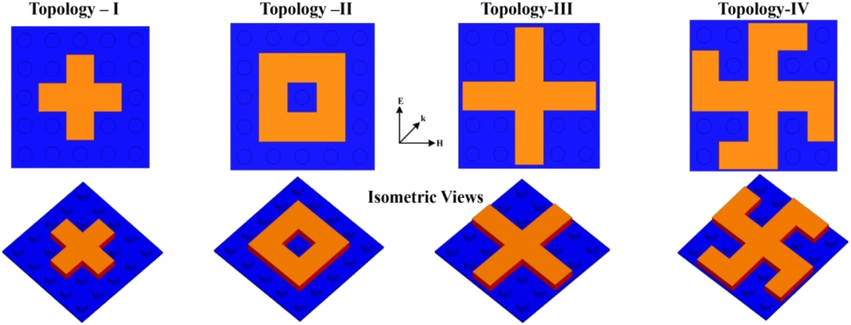
Topologies of the proposed reconfigurable absorber.
The structural parameters of the mounting board and the block mounts are illustrated in Figures 2 and 3, respectively. PLA (Polylactic Acid) material, with a dielectric constant of 2.1 and a loss tangent of 0.07, is chosen as the substrate material (highlighted in blue in Figure 2). PLA is widely used in 3D printing technology due to its popularity, low cost, biodegradability, and durability, and it is utilized here for fabricating prototypes.
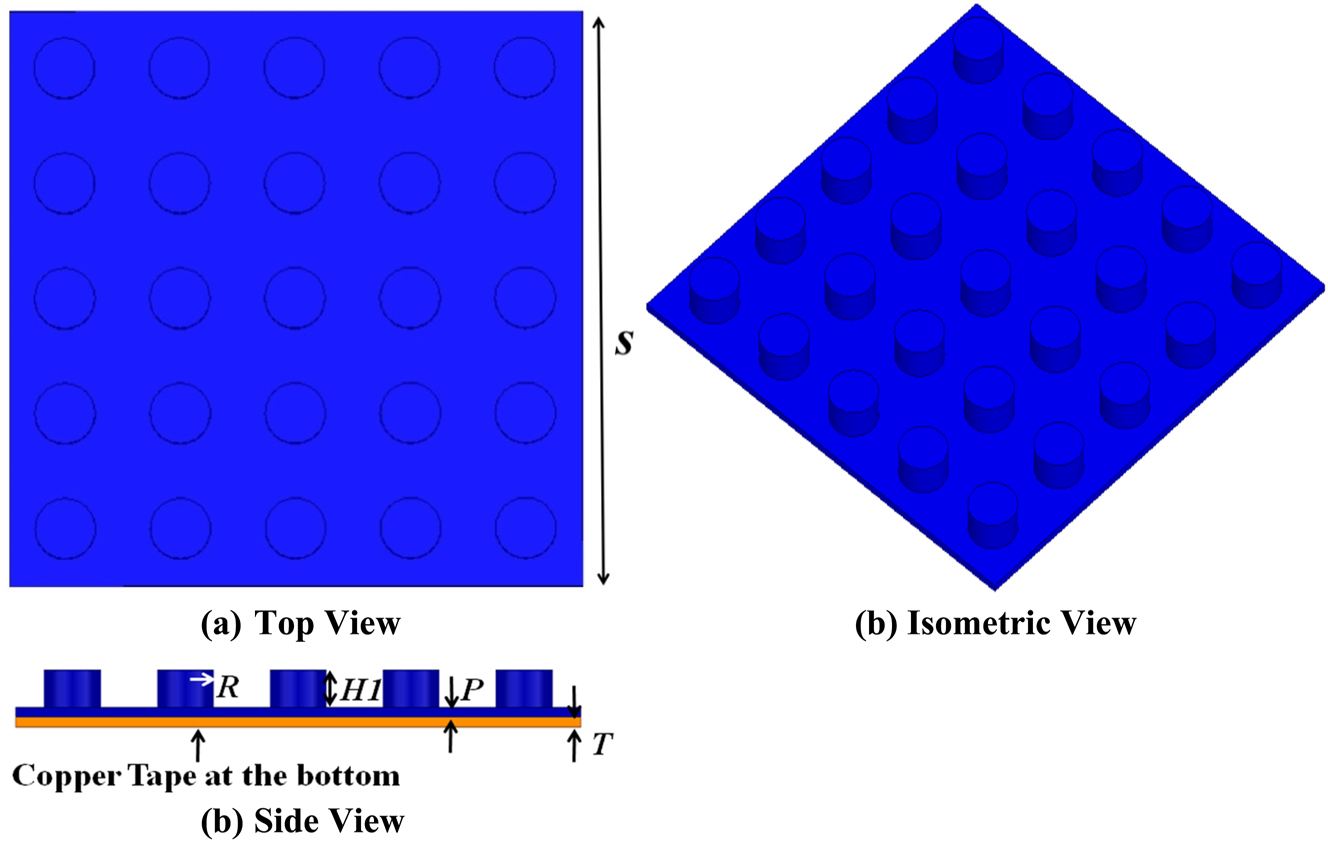
Structural parameters of mounting board: S = 40 mm, R = 2.1 mm, H1 = 1.7 mm, P = 0.4 mm and T = 0.065 mm.

Interlocking block mounts (in mm) A = 24, B = 8, C = 37.7, D = 16, E = 4.44, F = 7.2, G = 38.5, H2 = 1.9, H3 = 1.8, H4 = 1.82, H5 = 1.8, H6 = 1.7.
Adhesive copper tape is applied to create the metal ground plane on the back side of the mounting board and to form the conducting patterns on the top of the block mounts. Metal lamination on the absorber’s backside ensures complete shielding, preventing electromagnetic transmission and enhancing absorption efficiency. The interlocking block mounts, depicted in Figure 3 (highlighted in red), feature square-shaped cavities on their backs. The dimensions and periodicities of these squares are carefully chosen to ensure proper interlocking with the circular studs on the mounting base. Detailed dimensions are provided in the figure captions.
The evolutionary process of mounting the interlocking block on the top of a mounting board and adhering copper tape on the back side of the mounting board and on the top ofthe block mounts is depicted in Figure 4(a). The resonating blocks, each with metal sheets realized using copper tape on the top, are uniformly placed in a periodic arrangement. In the first case, topology I is placed periodically, while in subsequent cases, the block mounts are replaced with corresponding topologies in a similar manner. The periodicity is identical for all four cases; hence, the unit cells are only studied during simulation. The simulated absorptivity and reflectivity curves of the combined structures (mounting boards and block mounts) are verified using the full-wave high-frequency structure simulator (HFSS) software, as shown in Figure 4(b). To simulate the unit cell as a two-dimensional periodic extension, master-slave boundary conditions are employed on the sidewalls, with excitation provided by a Floquet port from the top side of the geometry. All four presented topologies are sequentially mounted on the mounting board, and their electromagnetic responses and footprint sizes are tabulated in Table 1. It is observed that the absorption frequency (as well as the full-width half-maximum bandwidth) gradually shifts from the higher side to the lower side (4.89 GHz–2.25 GHz) as the topology changes from I to IV. This shift is due to the increase in effective metallic length and the corresponding decrease in frequency. However, the absorption magnitude remains near unity in all four cases.
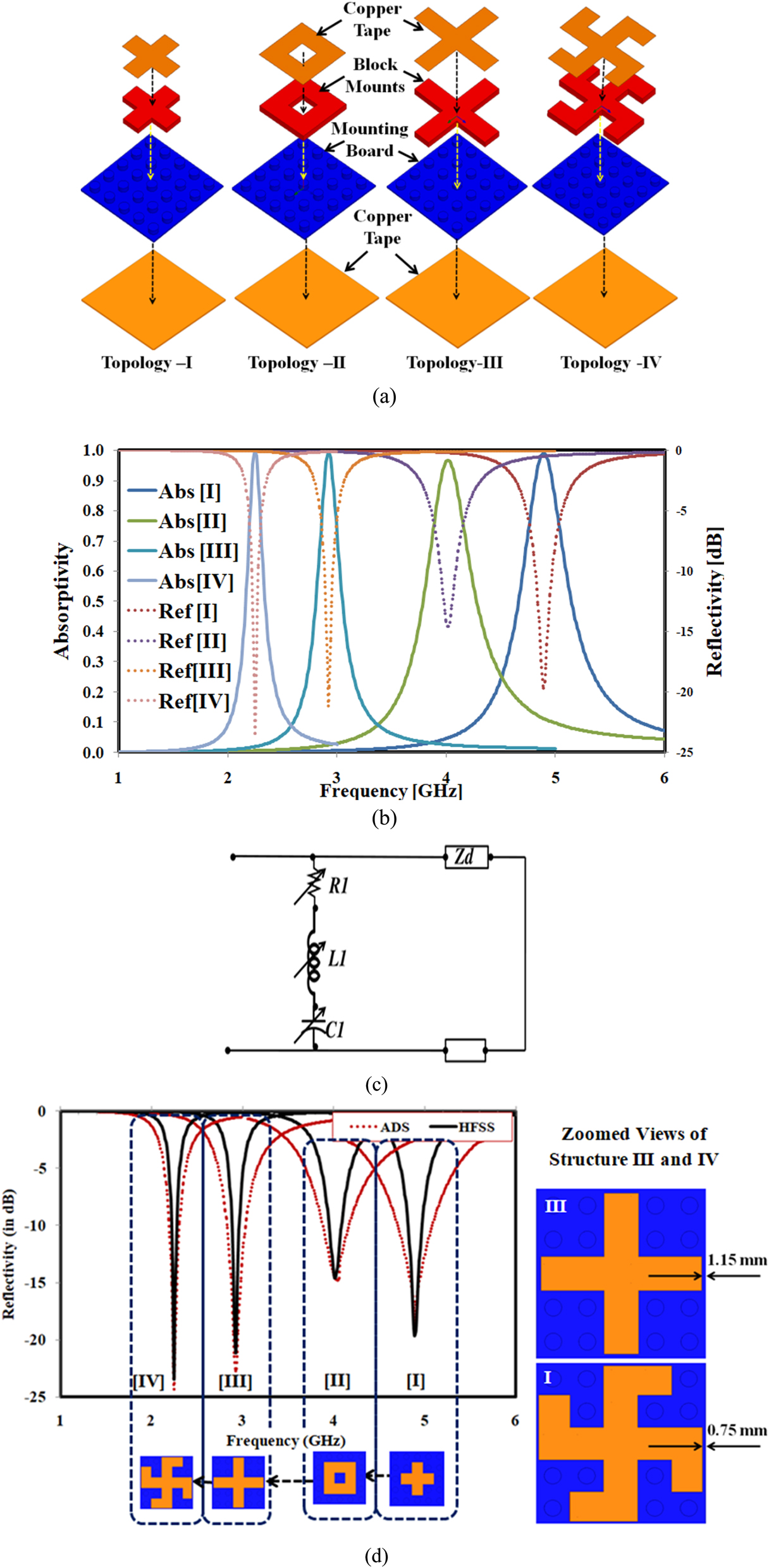
Overview and analysis of the proposed FSS absorber design. (a) Evolutionary process of the proposed FSS absorber using interlocking structures. (b) Absorptivity and reflectivity curves for each proposed topology of the FSS absorber. (c) Equivalent circuit model representation. (d) Comparison of the equivalent circuit model response with the simulated results for the absorber.
Absorptivity, reflection coefficient, FWHM bandwidth, unit cell thicknesses and sizes for all the four topologies.
| Topology | Resonant frequency [GHz] | Absorptivity [%] | Reflection coefficient [in dB] | Full width half maximum band width [FWHM] |
Thickness of unit cell (in terms of λ) | Electrical size of unit cell (in λ × λ) |
|---|---|---|---|---|---|---|
| I | 4.89 | 98.92 | −19.66 | 4.66 GHz–5.14 GHz (480 MHz) | 0.037 | 0.653 × 0.653 |
| II | 4.02 | 96.52 | −14.57 | 3.78 GHz–4.27 GHz (490 MHz) | 0.029 | 0.536 × 0.536 |
| III | 2.92 | 99.33 | −21.13 | 2.82 GHz–3.06 GHz (240 GHz) | 0.021 | 0.389 × 0389 |
| IV | 2.25 | 99.55 | −23.45 | 2.16 GHz–2.34 GHz (180 MHz) | 0.016 | 0.300 × 0.300 |
The equivalent circuit model of the presented absorber design is shown in Figure 4(c). L1 represents the variable inductance corresponding to the lengths of the resonators, which are realized by block mounts on the top of the structure. Rearranging the block mounts into different topological shapes, which alters the patch length, leads to a change in the equivalent inductance. R1 accounts for the variable resistance resulting from the finite conductivity of the top copper metal, representing minimal ohmic losses. C1 denotes the variable capacitance between adjacent unit cells. The dielectric substrate is modeled as a transmission line, with the bottom metal plane considered a short circuit.
While varying the block mounts for different topologies I to IV without disturbing the base of the mounting board, a variation in the circuit parameters (L1, R1, and C1) takes place, and the absorption frequency is shifted accordingly. The circuit values of the equivalent circuit model (ECM) were obtained using the curve-fitting technique in the Advanced Design System (ADS) software, as presented in Table 2, since no closed-form expression is available to derive the circuit parameters for the designed geometries (like Swastika). The process involved the following steps:
Initial Parameter Estimation: The circuit parameter values have initially been estimated based on the topologies and their geometric dimensions. The inductance (L1) value has been estimated based on the length of the resonator arms along the direction of electric field, The capacitance (C1) value has been determined by the physical separation between adjacent unit cells, whereas the resistance (R1) has been obtained from the ohmic losses caused by the finite conductivity of the copper layer. Standard equations from the reference articles [28], [37], [38], [39] were used, providing an initial range for the parameter values for all configurations (I to IV).
Simulation and Optimization in ADS: Then the absorber structures have been simulated in ADS software using the curve-fitting method. This process involves with adjusting the circuit model parameter values (L1, R1, C1) to align the frequency response of the ECM with the simulated result obtained from HFSS. The software optimizes the circuit parameters by minimizing the error between the simulated reflection/absorption curve and the theoretical curve derived from the ECM. It is noteworthy that the optimization might have generated different sets of possible circuit parameters; however, we have chosen the closest ones to our initial estimated values.
Validation of Circuit Values: Once the optimized values for L1, R1, and C1 are obtained for each configuration, the circuit model has been validated by comparing the ECM responses with their respective full-wave simulations. The close agreement between these results, as shown in Figure 4(d) in the revised manuscript, confirms the accuracy of the ECM.
Optimized circuit parameters of equivalent circuit.
| Topology | Resonant frequency [GHz] | Resistance (R1 in ohms) | Inductance (L1 in nH) | Capacitance (C1 in pF) |
|---|---|---|---|---|
| I | 4.89 | 16 | 0.25 | 0.35 |
| II | 4.02 | 8.5 | 0.051 | 0.57 |
| III | 2.92 | 7.68 | 1.0 | 0.80 |
| IV | 2.25 | 4.4 | 1.15 | 1.3 |
3 Performance investigation
Figure 5 illustrates the performance of the proposed reconfigurable absorber assembled with block mounts molded in the shape of presented topologies under varied incidence and polarization angles. Constant absorption responses for the polarization angles ranging from 0° to 90° is observed for all the four topologies as illustrated in Figure 5(a–d). Under transverse electric (TE) polarization, as shown in Figure 5(e−h), and transverse magnetic (TM) polarization, as shown in Figure 5(i–l), the resonant frequency remains stable for angle variations up to 45°. Further increases in angle affect the absorptivity and cause slight frequency shifts in either direction. However, it is observed from the figures that the responses in TM mode are less stable than those in TE mode; small shifts in frequencies with increasing incidence angle are more evident in TM mode.
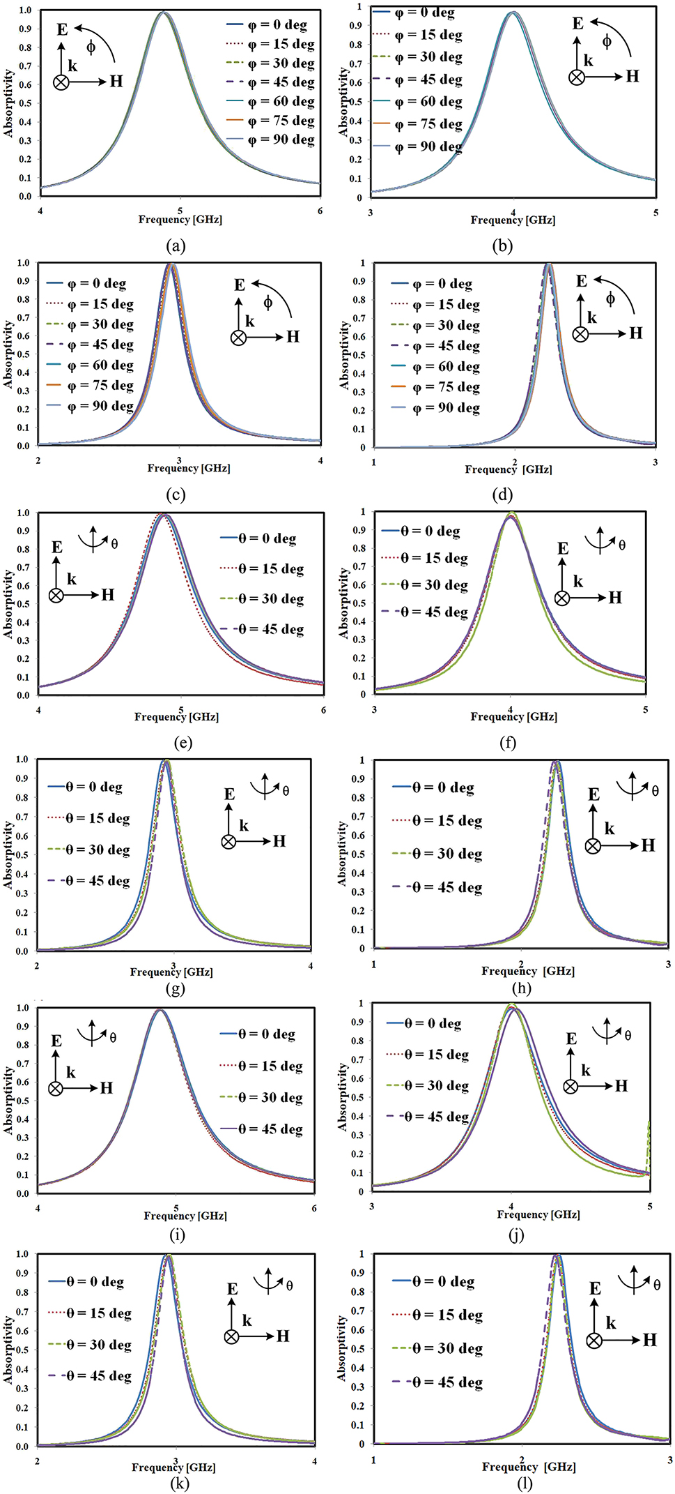
Simulated absorptivity curves at various polarization angles for topologies (a) I, (b) II, (c) III and (d) IV, simulated responses for absorptivity at various oblique incidence angles for topologies (e) I, (f) II, (g) III and (h) IV under TE and TM polarization simulation responses for Topologies (i) I, (j) II, (k) III and (l) IV.
The impedance curves (real and imaginary) of the presented FSS absorber are illustrated in Figure 6(a–d), and the values of the real and imaginary impedances at the corresponding resonant frequencies for all four topologies are tabulated in Table 3.
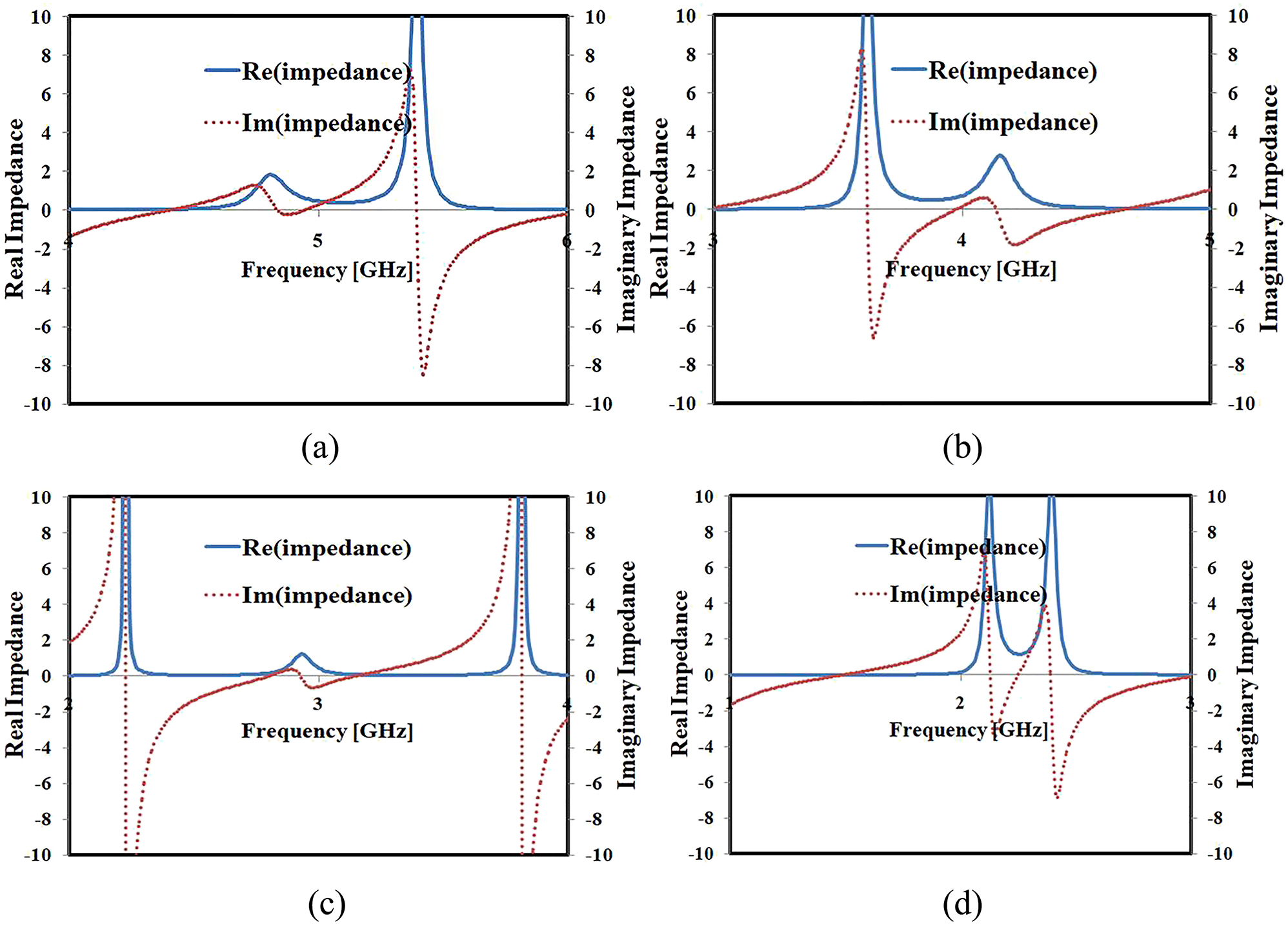
Impedance curves of the proposed topologies (a) I (b) II (c) III and (d) IV.
Values of real and imaginary impedances for all the four topologies.
| Topology | Resonant frequency [GHz] | Real (Z) | Imaginary (Z) |
|---|---|---|---|
| I | 4.89 | 0.98 | −0.20 |
| II | 4.02 | 0.81 | 0.29 |
| III | 2.92 | 1.19 | −0.31 |
| IV | 2.25 | 1.13 | 0.03 |
It is observed that the imaginary impedance values are close to zero, and the real impedance values are close to one, confirming impedance matching and thus minimal reflection and maximum absorption at the resonant frequencies of the corresponding resonators. The electric field (E-field) and surface current distributions for all four topologies of the designed FSS absorber at resonance frequencies are studied and shown in Figure 7(a–d). The electric resonance originates from the conductive top patterns, while the magnetic resonance is generated by the loop of anti-parallel currents flowing in the top and bottom conducting sheets of the presented absorber. This confirms the maximum absorption characteristics of the FSS-based absorber at resonating frequencies.
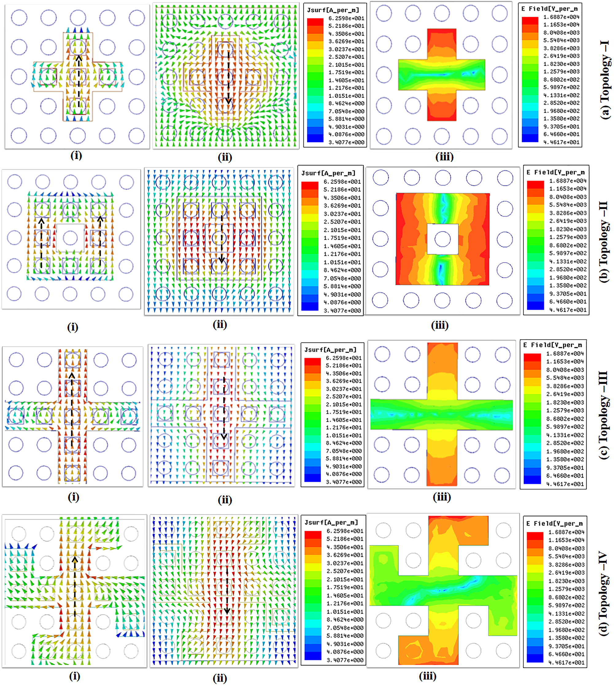
Surface current distribution at (i) top surface (ii) bottom surface (iii) electric field distribution at absorption peaks.
4 Fabrication and testing process
The validity of the simulated responses has been confirmed by fabricating prototypes of the proposed FSS-based absorber built with interlocking blocks, as depicted in Figure 8. A blue-colored mounting board measuring 240 mm × 240 mm, featuring circular studs elevated on it, has been fabricated using 3-D printing technology. The block mounts are 3-D printed with red-colored PLA filament in various topological shapes, with adhesive copper tape (0.065 mm thick) applied to their top surfaces for conductivity. Additional copper tape is affixed to the back side of the mounting board. Edge cutting of the copper tape was performed using the Skycut C24 vinyl cutter for precision.
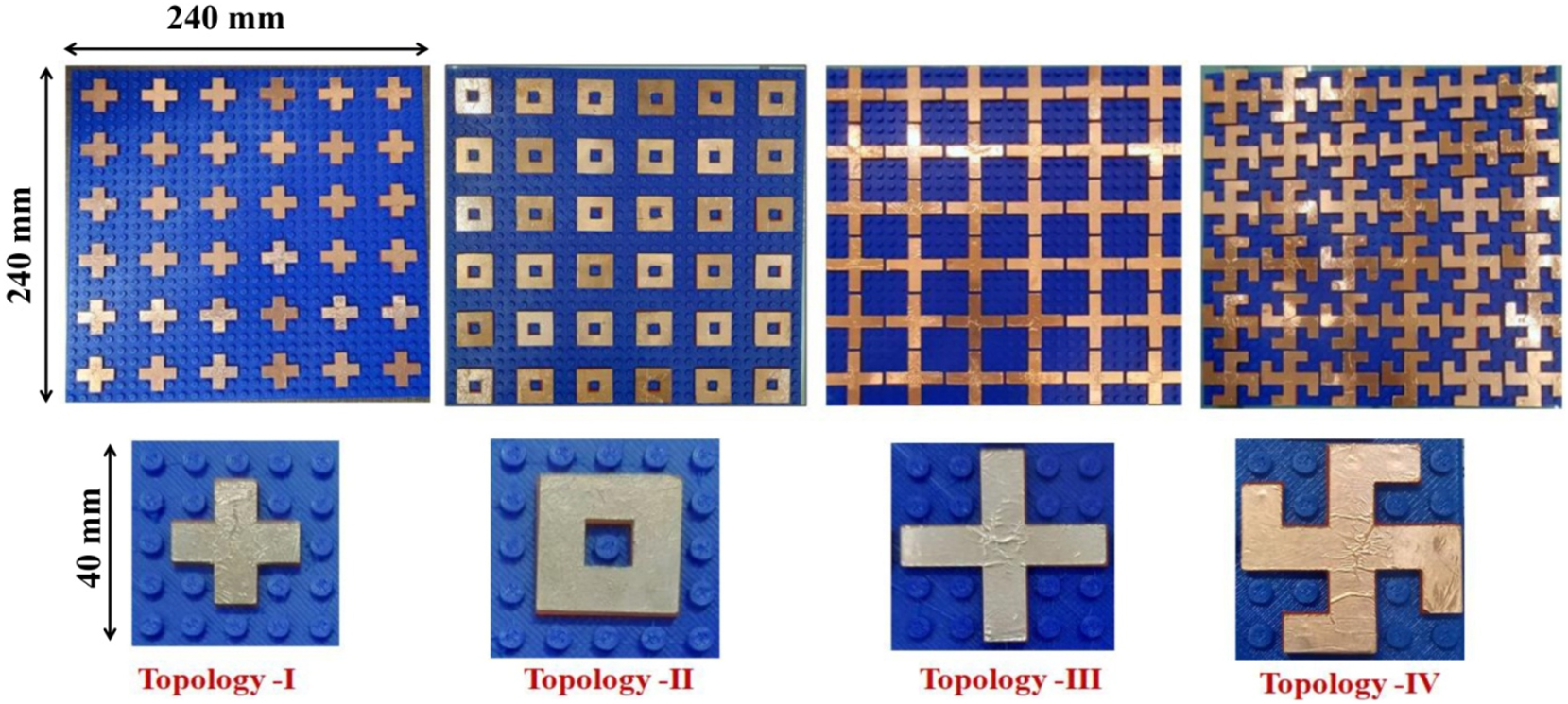
Pictures of fabricated prototype of the proposed designs (240 × 240 square mm).
The dielectric structures were printed using the Pratham 6.0 3D printer from Make3D.in. A total of 36 blocks of each topological shape were fabricated and mounted on different occasions to achieve mechanical reconfigurability, as shown in Figure 8.
The measurements were conducted using the free-space method. The measurement setup consisted of a pair of horn antennas – one serving as a transmitter and the other as a receiver – both connected to an Anritsu S820E vector network analyzer. To minimize edge diffraction effects, a tailor-made absorbing wall frame surrounded the prototype during measurements. Reflection coefficients from the structures were measured by the antennas, and these coefficients were converted to absorption magnitudes during plotting (since transmission is zero due to the metal backing). Initially, the absorption properties of a copper plate were measured, and then the plate was replaced with the fabricated prototypes for subsequent measurements. The response obtained from the copper plate was used to normalize the absorption performances of the structures, thereby canceling out propagation losses and other factors.
Figure 9(a–d) illustrate measurement set ups and Figure 10(a–d) depicts the comparative graphical representations of the measurement responses to that of the simulated ones for different cases and they appear to be in good agreement with each other. During the normal incidence, two antennas have been placed in close proximity, whereas both antennas have been rotated in an arc to measure the response under oblique incidence. Although the simulation analysis demonstrated angular stability up to 45°, the absorption characteristics were measured under TE mode only up to a 30° angle due to experimental limitations. However, a good agreement is observed, except for a slight frequency shift as the angle of incidence increases.
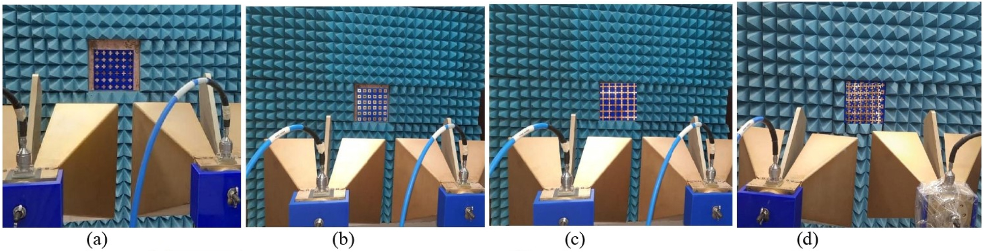
Experimental set up for topologies (a) I, (b) II, (c) III, (d) IV.
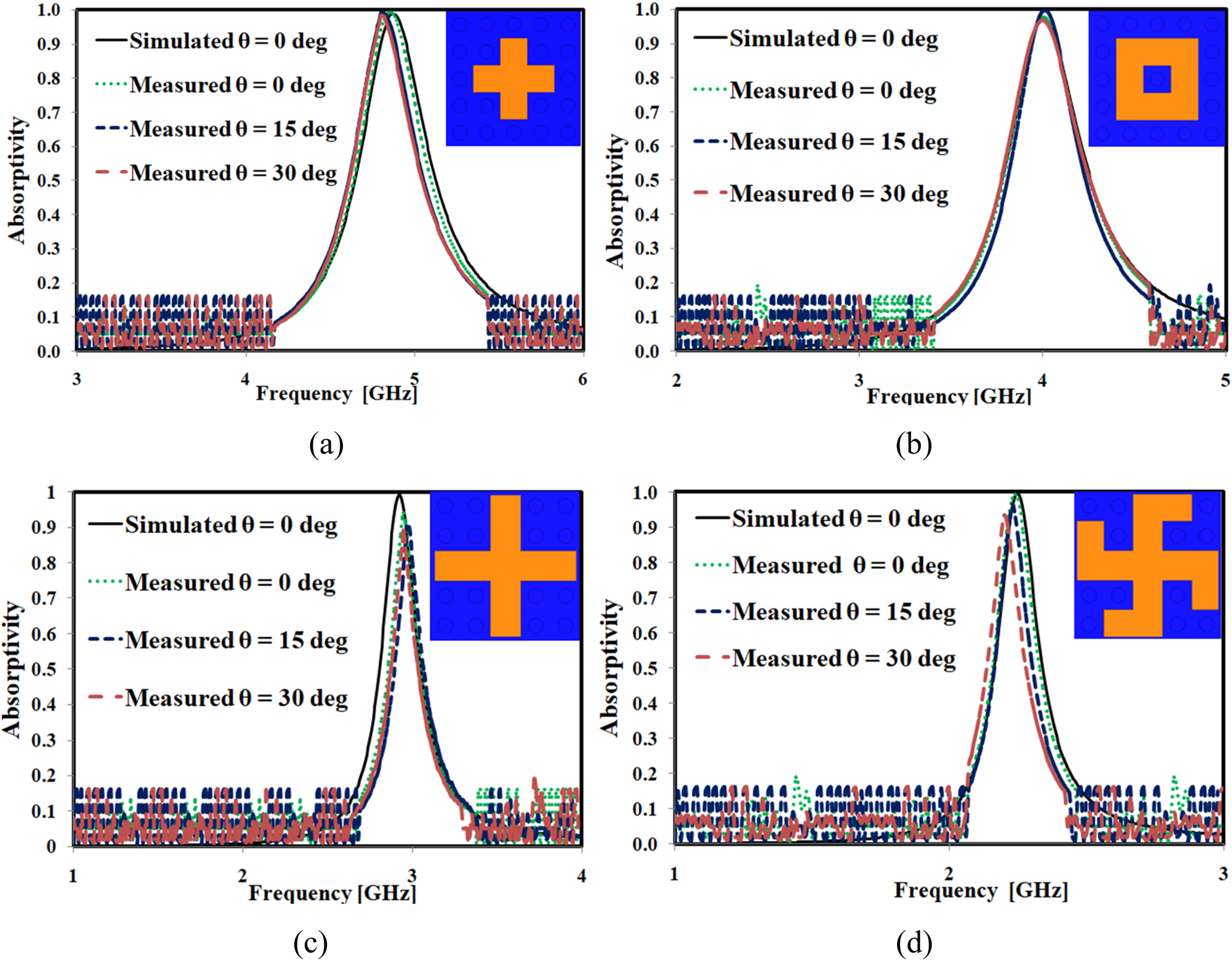
Comparative graphical representations of the simulated and measured responses (a) I (b) II (c) III and (d) IV.
The comparative study of the proposed work with formerly published research on mechanical and electrical reconfiguration techniques is detailed in Table 4. The proposed absorber achieves significant reductions in thickness and overall electrical size across all topologies, resulting in a miniaturized structure when compared to other mechanically reconfigurable designs. However, compared to designs employing electrical reconfiguration techniques, the presented absorber demonstrates a simpler configuration without the need for complex biasing networks and embedded circuitry, which are typical in those compact designs but increase structural complexity. Despite this advantage, there is a compromise in terms of the electrical size of the presented absorber compared to designs using electrical reconfiguration techniques. The presented work justifies a cheaper, simpler-to-design-and-fabricate, reusable, and easy-to-reconfigure approach for the design of an FSS-based absorber compared to previously published methods. This approach avoids complex mechanical alterations, the use of active elements, and additional biasing networks.
Comparative study of the proposed work with formerly published reconfigurable structures.
| Ref.; year |
Shape of FSS | Method adopted to achieve the reconfigurability | Fabrication method | Material used | Topology | Thickness of unit cell (in terms of λ) | Physical size of unit cell (in mm × mm) | Electrical size of unit cell (in λ × λ) | Frequency bands |
|---|---|---|---|---|---|---|---|---|---|
| This work | 3D printed mounting board, on which different blocks can be attached using interlocking studs | Mechanical: changing various resonating blocks on the board | 3D printing | PLA (∈ r = 2.1 & tan δ = 0.07) + copper tape | I. Cross dipole | 0.037 | 40 × 40 | 0.653 × 0.653 | S and C bands |
| II. Loop | 0.029 | 0.536 × 0.536 | |||||||
| III. Cross dipole with ext. arm length | 0.021 | 0.389 × 0389 | |||||||
| IV. Swastika | 0.016 | 0.300 × 0.300 | |||||||
| [10]; 2023 |
Combination of triangular loop and three-legged ele. | Altering the angle of incidence | PCB technology | FR4 (∈ r = 4.4 & tan δ = 0.02) | NAa | 0.042 | 14 × 14 | 0.394 × 0.394 | X-band |
| [20]; 2022 |
Two periodically arranged metallic patterns on both sides of FR4 substrate | Electrical: using p-i-n diode | PCB technology | FR4 (∈ r = 4.4 & tan δ = 0.02) | NA | 0.028 | 10 × 10 | 0.187 × 0.187 | C-band |
| [14]; 2021 |
Rectangular strips | Electrical: using varactor diode | PCB technology | F4B(∈ r = 2.65 & tan δ = 0.001) | NA | 0.008 | 10 × 10 | 0.141 × 0.141 | S and C-bands |
| [34]; 2021 |
Reusable building blocks (RBB) | Mechanical: relocating the RBB | 3D printing | ABS (∈ r = 2.8 & tan δ = 0.005) + copper tape |
Square plate (SP) | 0.117 | 39 × 39 | 1.014 × 1.014 | C-band |
| Cross plate (CP) | 0.084 | 0.731 × 0.731 | |||||||
| CP (miniaturized) | 0.106 | 0.539 × 0.539 | |||||||
| [35]; 2021 |
Lego type blocks | Mechanical: rearranging the lego blocks | 3D printing | (∈ r = 2.6 & tan δ = 0.002) + metal with surf. imp. (0.5 Ω/sq) | Cross dipole | 0.165 | 24 × 24 | 0.567 × 0.567 | C and X bands |
| Dipole | 0.218 | 0.750 × 0.750 | |||||||
| [15]; 2020 |
Square slot | Electrical: using varactor diode | PCB technology | Rogers 4350B (∈ r = 3.48) | Sample 2 | 0.008 | 9 × 9 | 0.147 × 0.147 | C- band |
| [33]; 2020 |
Cross dumb-bell | Mechanical: manual rotation of horizontal grid | Polyester sheet | (∈ r = 2.8 and tan δ = 0.0045) | NA | 0.001 | 18 × 18 | 0.192 × 0.192 | S and C-bands |
| [16]; 2020 |
Rectangular loop with plus shaped resonators | Electrical: using varactor diode | Additive manufacturing | PET (∈ r = 3.9) + silver ink | NA | 0.001 | 6 × 6 | 0.07 × 0.07 | S and C-bands |
| [17]; 2019 |
Jerusalem cross on opposite sides of dielectric substrate | Electrical: using p-i-n and varactor diode | PCB technology | FR4 | NA | 0.014 | 10 × 10 | 0.123 × 0.123 | S and C-bands |
-
aNA = not applicable. Bold values indicate findings from the current study, distinguishing them from previously published structures to emphasize the contributions and novelty of this work.
5 Conclusions
This paper presents a simple, cost-effective, and straightforward method for designing a reconfigurable FSS-based absorber using 3D printed interlocking blocks. A mounting board and four differently shaped block-mounts are designed, printed, and validated through simulation and experimental study. The assembly of the 3D printed board and block-mounts is found to be easy to operate, reusable, and low-cost compared to conventional PCB-fabricated prototypes. The novel concept of achieving reconfigurability by mechanically relocating differently shaped block-mounts is introduced. With a diverse selection of block mounts and their reusable properties, these geometries can be applied across various radar cross-section applications, particularly those where response time flexibility is crucial.
Acknowledgments
The authors acknowledge the support of Applied Electromagnetic Laboratory of IIT Indore for providing testing and measurement facilities and AICTE IDEA Lab, Acropolis, Indore for fabrication resources.
-
Research ethics: Not applicable.
-
Informed consent: Not applicable.
-
Author contributions: The authors have accepted responsibility for the entire content of this manuscript and approved its submission.
-
Use of Large Language Models, AI and Machine Learning Tools: None declared.
-
Conflict of interests: The authors state no conflict of interest.
-
Research funding: None declared.
-
Data availability: Not applicable.
References
[1] X Lv, R. T. Ako, M. Bhaskaran, S. Sriram, C. Fumeaux, and W. Withayachumnankul, “Frequency-selective-surface-based mechanically reconfigurable terahertz bandpass filter,” IEEE Trans. Terahertz Sci. Technol., vol. 12, no. 3, pp. 257–266, 2022, https://doi.org/10.1109/TTHZ.2022.3148816.Suche in Google Scholar
[2] S. Ghosh, “Active metamaterial frequency selective surface (FSS) based tunable radar absorbing structure (RAS),” Handb. Metamaterial-Derived Freq. Sel. Surface., vol. 3, pp. 149–190, 2023, https://doi.org/10.1007/978-981-16-6441-0_5.Suche in Google Scholar
[3] H. A. Mohamed, M. Edries, M. A. Abdelghany, and A. A. Ibrahim, “Millimeter-wave antenna with gain improvement utilizing reflection FSS for 5-G networks,” IEEE Access, vol. 10, pp. 73601–73609, 2022, https://doi.org/10.1109/ACCESS.2022.3189651.Suche in Google Scholar
[4] M. A. Shukoor and S. Dey, “Novel miniaturized arrow linked figure of eight square loop FSS-based multiband linear-circular and linear-cross reflective microwave polarizer,” Int. J. Microw. Wirel. Technol., vol. 15, no. 4, pp. 591–599, 2023. https://doi/10.1017/S1759078722000976.10.1017/S1759078722000976Suche in Google Scholar
[5] B. Jiang, H. Hu, J. Tian, S. Lei, M. Chen, and B. Chen, “A polarization-insensitive Dual-Band FSS with high selectivity and independently switchable characteristics,” IEEE Antenn. Wirel. Propag. Lett., vol. 22, no. 1, pp. 14–18, 2022. https://doi/10.1109/LAWP.2022.3199565.10.1109/LAWP.2022.3199565Suche in Google Scholar
[6] S. Kundu and A. Chatterjee, “A new compact ultra-wideband frequency selective surface with angular stability and polarization independence for antenna radiation enhancement in microwave imaging application,” AEU Int. J. Electron. Commun., vol. 155, 2022, Art. no. 154351, https://doi.org/10.1016/j.aeue.2022.154351.Suche in Google Scholar
[7] W. Y. Yong and A. A. Glazunov, “Miniaturization of a fully metallic bandpass frequency selective surface for millimeter-wave band applications,” IEEE Trans. Electromagn. Compat., vol. 65, no. 4, pp. 1072–1080, 2023, https://doi.org/10.1109/temc.2023.3283352. https://doi/10.1109/TEMC.2023.3283352.Suche in Google Scholar
[8] M. Z. Hlaing, et al.., “3D micro structured frequency selective surface based on carbonized polyimide films for terahertz applications,” Adv. Opt. Mater., vol. 10, no. 8, 2022, Art. no. 2102178, https://doi.org/10.1002/adom.202102178.Suche in Google Scholar
[9] J. Li, et al.., “High angular stability and polarization insensitive optically transparent bandpass frequency selective surface based on micro copper mesh,” Opt. Commun., vol. 536, 2023, Art. no. 129365, https://doi.org/10.1016/j.optcom.2023.129365.Suche in Google Scholar
[10] A. Antony, S. Dutta, B. Dasgupta, and A. Bhattacharya, “Reconfigurable frequency selective surfaces for X Band applications,” Prog. Electromagn. Res. C, vol. 132, pp. 79–88, 2023, https://doi.org/10.2528/PIERC23030304.Suche in Google Scholar
[11] Z. Xue, S. Zhong, and Y. Ma, “Graphene-FSS hybrid absorptive structure with amplitude/frequency dual-modulated passband,” IEEE Antenn. Wirel. Propag. Lett., vol. 20, no. 9, pp. 1711–1715, 2021. https://doi/10.1109/LAWP.2021.3094835.10.1109/LAWP.2021.3094835Suche in Google Scholar
[12] M. A. Shukoor and S. Dey, “Wideband reconfigurable multifunctional absorber/reflector with bandpass/bandstop filtering and band-notch absorption for RCS and EMI shielding,” IEEE Trans. Electromagn. Compat., vol. 28, 2023. https://doi/10.1109/TEMC.2023.3306019.10.1109/TEMC.2023.3306019Suche in Google Scholar
[13] J. Sun, Q. Cao, Y. Li, and H. Li, “Functional reconfigurable integrated structure of circularly polarized antenna and FSS absorber,” IEEE Trans. Antenn. Propag., vol. 69, no. 11, pp. 7260–7268, 2021. https://doi/10.1109/TAP.2021.3076168.10.1109/TAP.2021.3076168Suche in Google Scholar
[14] H. Bai, et al.., “Tunable frequency selective surface with angular stability,” IEEE Antenn. Wirel. Propag. Lett., vol. 20, no. 6, pp. 1108–1112, 2021, https://doi.org/10.1109/LAWP.2021.3073907.Suche in Google Scholar
[15] M. Guo, et al.., “Analysis and design of a high-transmittance performance for varactor-tunable frequency-selective surface,” IEEE Trans. Antenn. Propag., vol. 69, no. 8, pp. 4623–4632, 2020. https://doi/10.1109/TAP.2020.3045517.10.1109/TAP.2020.3045517Suche in Google Scholar
[16] T. Tian, et al.., “Flexible and reconfigurable frequency selective surface with wide angular stability fabricated with additive manufacturing procedure,” IEEE Antenn. Wirel. Propag. Lett., vol. 19, no. 12, pp. 2428–2432, 2020. https://doi/10.1109/LAWP.2020.3034944.10.1109/LAWP.2020.3034944Suche in Google Scholar
[17] R. Phon, S. Ghosh, and S. Lim, “Active frequency selective surface to switch between absorption and transmission band with additional frequency tuning capability,” IEEE Trans. Antenn. Propag., vol. 67, no. 9, pp. 6059–6067, 2019, https://doi.org/10.1109/TAP.2019.2916752.Suche in Google Scholar
[18] H. Ali, L. Riaz, S. A. M. Kirmani, S. A. Khan, and M. F. Shafique, “Dual Bandstop reconfigurable (Switchable) frequency Selective surface for WLAN applications at 2.4 and 5 GHz,” AEU Int. J. Electron. Commun., vol. 143, 2022, Art. no. 154038, https://doi.org/10.1016/j.aeue.2021.154038.Suche in Google Scholar
[19] S. C. Bakshi, D. Mitra, and F. L. Teixeira, “FSS-based fully reconfigurable rasorber with enhanced absorption bandwidth and simplified bias network,” IEEE Trans. Antenn. Propag., vol. 68, no. 11, pp. 7370–7381, 2020. https://doi/10.1109/TAP.2020.3008615.10.1109/TAP.2020.3008615Suche in Google Scholar
[20] P. M. Megh Sainadh, A. Sharma, and S. Ghosh, “Polarization-insensitive absorptive/transmissive reconfigurable frequency selective surface with embedded biasing,” IEEE Antenn. Wirel. Propag. Lett., vol. 22, no. 1, pp. 164–168, 2022, https://doi.org/10.1109/LAWP.2022.3206098.Suche in Google Scholar
[21] X. Chen, J. Gao, C. Fang, N. Xu, Y. Wang, and Y. Tang, “Deformable frequency selective surface structure with tuning capability through thermoregulating,” Opt. Express, vol. 23, no. 12, pp. 16329–16338, 2015, https://doi.org/10.1364/OE.23.016329.Suche in Google Scholar PubMed
[22] M. Li, B. Yu, and N. Behdad, “Liquid-tunable frequency selective surfaces,” IEEE Microw. Wirel. Compon. Lett., vol. 20, no. 8, pp. 423–425, 2010, https://doi.org/10.1109/LMWC.2010.2049257.Suche in Google Scholar
[23] K. Fuchi, Junyan Tang, B. Crowgey, A. R. Diaz, E. J. Rothwell, and R. O. Ouedraogo, “Origami tunable frequency selective surfaces,” IEEE Antenn. Wirel. Propag. Lett., vol. 11, pp. 473–475, 2012. https://doi/10.1109/LAWP.2012.2196489.10.1109/LAWP.2012.2196489Suche in Google Scholar
[24] L. Kang, Q. Zhao, H. Zhao, and J. Zhou, “Magnetically tunable negative permeability metamaterial composed by split ring resonators and ferrite rods,” Opt. Express, vol. 16, no. 12, pp. 8825–8834, 2008, https://doi.org/10.1364/OE.16.008825.Suche in Google Scholar
[25] M. Gil, et al.., “Electrically tunable split-ring resonators at microwave frequencies based on barium-strontium-titanate thick films,” Electron. Lett., vol. 45, no. 8, pp. 417–418, 2009. https://doi/10.1049/el.2009.3055.10.1049/el.2009.3055Suche in Google Scholar
[26] R. J. Langley and E. Parker, “Frequency-selective surfaces on biased ferrite substrates,” Electron. Lett., vol. 30, no. 15, pp. 1193–1194, 1994. https://doi/10.1049/el:19940823.10.1049/el:19940823Suche in Google Scholar
[27] Y. Zhang, Y. Feng, B. Zhu, J. Zhao, and T. Jiang, “Graphene based tunable metamaterial absorber and polarization modulation in terahertz frequency,” Opt. Express, vol. 22, no. 19, pp. 22743–22752, 2014, https://doi.org/10.1364/OE.22.022743.Suche in Google Scholar PubMed
[28] S. Ghosh and S. Lim, “Fluidically-reconfigurable multifunctional frequency selective surface with miniaturization characteristic,” IEEE Trans. Microw. Theor. Techn., vol. 66, no. 8, pp. 3857–3865, 2018, https://doi.org/10.1109/TMTT.2018.2829195.Suche in Google Scholar
[29] S. Ghosh and S. Lim, “A multifunctional reconfigurable frequency-selective surface using liquid-metal alloy,” IEEE Trans. Antenn. Propag., vol. 66, no. 9, pp. 4953–4957, 2018. https://doi/10.1109/TAP.2018.2851455.10.1109/TAP.2018.2851455Suche in Google Scholar
[30] D. Ferreira, I. Cuiñas, R. F. S. Caldeirinha, and T. R. Fernandes, “3-D mechanically tunable square slot FSS,” IEEE Trans. Antennas Propag., vol. 65, no. 1, pp. 242–250, 2017. https://doi.org/10.1109/TAP.2016.2631131.Suche in Google Scholar
[31] R. Sivasamy, B. Moorthy, M. Kanagasabai, V. R. Samsingh, and M. G. N. Alsath, “A wideband frequency tunable FSS for electromagnetic shielding applications,” IEEE Trans. Electromagn. Compat., vol. 60, no. 1, pp. 280–283, 2018, https://doi.org/10.1109/TEMC.2017.2702572.Suche in Google Scholar
[32] S. N. Azemi, K. Ghorbani, and W. S. T. Rowe, “A reconfigurable FSS using a spring resonator element,” IEEE Antenn. Wirel. Propag. Lett., vol. 12, pp. 781–784, 2013. https://doi/10.1109/LAWP.2013.2270950.10.1109/LAWP.2013.2270950Suche in Google Scholar
[33] A. N. Silva, et al.., “Simple and efficient design of reconfigurable FSS with triangular patch elements,” in 2017 International Applied Computational Electromagnetics Society Symposium-Italy (ACES), Firenze, IEEE, 2017, pp. 1–2.10.23919/ROPACES.2017.7916055Suche in Google Scholar
[34] S. A. B, E. F. Sundarsingh, and V. S. Ramalingam, “Mechanically reconfigurable frequency selective surface for RF shielding in indoor wireless environment,” IEEE Trans. Electromagn. Compat., vol. 62, no. 6, pp. 2643–2646, 2020, https://doi.org/10.1109/TEMC.2020.2983899.Suche in Google Scholar
[35] H. Li, et al.., “Simple, low-cost, and reconfigurable metamaterials and metasurfaces based on reusable building blocks: a proposed approach,” IEEE Antenn. Propag. Mag., vol. 65, no. 1, pp. 40–48, 2021, https://doi.org/10.1109/MAP.2021.3110482.Suche in Google Scholar
[36] S. S. Cho and I. P. Hong, “Design of assembly‐type frequency selective surface structure using Lego‐type blocks,” Microw. Opt. Technol. Lett., vol. 64, no. 2, pp. 288–293, 2022, https://doi.org/10.1002/mop.33104.Suche in Google Scholar
[37] R. J. Langley and E. A. Parker, “Equivalent circuit model for arrays of square loops,” Electron. Lett., vol. 18, no. 7, pp. 294–296, 1982, https://doi.org/10.1049/el:19820201.10.1049/el:19820201Suche in Google Scholar
[38] D. M. Pozar, Microwave Engineering, New York, NY, USA, Wiley, 2011.Suche in Google Scholar
[39] O. Luukkonen, et al.., “Simple and accurate analytical model of planar grids and high-impedance surfaces comprising metal strips or patches,” IEEE Trans. Antennas Propag., vol. 56, no. 6, pp. 1624–1632, 2008, https://doi.org/10.1109/TAP.2008.923327.Suche in Google Scholar
© 2024 Walter de Gruyter GmbH, Berlin/Boston
Artikel in diesem Heft
- Frontmatter
- Research Articles
- Reconfigurable frequency selective surface based absorber realized using interlocking blocks
- Dual band beam steering antenna using branch line coupler network for higher band applications
- High-efficiency quad-band RF energy harvesting system with improved cross-coupled differential-drive rectifier
- A novel miniaturized microstrip filtering power divider with high selectivity based on composite right/left-handed (CRLH) concept
- High-selectivity wideband bandpass filter based on quintuple-mode stub-loaded resonator and defected ground structures
- Design of a high selective triple band integrated reconfigurable filtering antenna for wideband and narrowband applications
- A novel ultra-wideband end-fire antenna based on spoof surface plasma polaritons
- Metamaterial-based transmit and receive antennas for wireless image transfer at 5.8 GHz
- Design of a MIMO implantable antenna with ultra-miniaturized volume and reduced SAR
- ANN modeling for predicting muscle-implanted antenna performance for skin and fat thickness variations at 2.45 GHz