
Theoretical background on semiconducting polymers and their applications to OSCs and OLEDs
-
Christine K. Luscombe
 ,
Uday Maitra
,
Uday Maitra
 ,
Michael Walter
und
Susanne K. Wiedmer
,
Michael Walter
und
Susanne K. Wiedmer

Abstract
Organic electronics has developed rapidly over the past 40 years. In 1977, a seminal discovery was reported that showed that a polymer known as polyacetylene could conduct electricity as well as metals could. This was a groundbreaking discovery that led to a Nobel Prize in Chemistry in 2000. The polymers that are used in organic electronics have now been widely studied for use in organic solar cells (OSCs), organic field effect transistors (OFETs), printable electronics, flexible electronics, antistatic coatings, actuators, and more recently in bioelectronics. In particular, the utility of organic electronics is seen in the commercial success of using organic electronic materials in organic light-emitting diodes (OLEDs) where OLED displays can be seen in mobile phones and as flat panel displays. In this paper, we provide a tutorial targeting upper secondary students describing how these special classes of polymers function, and how they can be synthesized. The paper further discusses the use of these materials in two applications: organic solar cells and organic light-emitting diodes. The paper ends with a brief discussion about hands-on activities that can be carried out in the upper secondary student science classroom.
Introduction
We currently live in an electronic world where we rely heavily on electronic devices for communication, national security, and personal health monitoring. With the advent of personalized healthcare and continuous health monitoring, there is a growing interest in wearable and stretchable electronic devices (Amjadi, Kyung, Park, & Sitti, 2016; Van Den Brand et al., 2015). While most of the existing technology currently relies on the use of inorganic materials, organic electronic materials offer an advantage in terms of being more eco-friendly and more affordable compared to their inorganic counterparts (Phan & Luscombe, 2019). Additionally, due to their intrinsic flexibility, stretchability, and softness, organic materials have the potential of enabling body-integrated devices. For example, one could consider using organic electronic materials as artificial skin with tactile sensitivity (Oh & Bao, 2019). Consumers are using organic electronic devices likely without being aware of it. For example, Samsung Galaxy cellphones have organic light-emitting diode (OLED)-based displays (Chen, Lee, Lin, Chen, & Wu, 2018). Furthermore, there are large area flat panel displays that are commercially available that are OLED-based. Our goal in this paper is to provide a tutorial targeting upper secondary (age group 14–18) students describing how these polymers work, how they are made, and how they operate in solar cells and OLEDs. We end by providing a brief description on hands-on activities.
Background on polymers and semiconducting polymers
The following sections focus on polymers, how semiconducting polymers differ from commodity polymers, why semiconducting polymers can absorb and emit visible light, and how polymers and semiconducting polymers differ in their synthetic methods. Polymers are a class of materials that are a little bit like spaghetti. They consist of long chain molecules known as macromolecules, and if you bring these macromolecules together, you get a polymer. A single spaghetti strand would be your macromolecule, and the bowl of spaghetti would be the polymer. Each macromolecule is made by connecting monomer molecules together. You could imagine stringing together small bits of macaroni to make something that resembles spaghetti. In this analogy, macaroni would be your monomer molecule. Examples of commonly used polymers include synthetic polymers such as polyethylene – used to make plastic bags, nylon – for making fibers for clothing or parachutes, and natural polymers including proteins, carbohydrates, and DNA.
Most polymers do not conduct electricity and are colorless. This is because the polymer backbone is comprised of single bonds (Figure 1a). If however, the polymer backbone is made up of alternating single and double bonds i.e., be π-conjugated (Figure 1b), the properties of the polymer change completely. The polymer can now conduct electricity and can absorb or emit visible light.
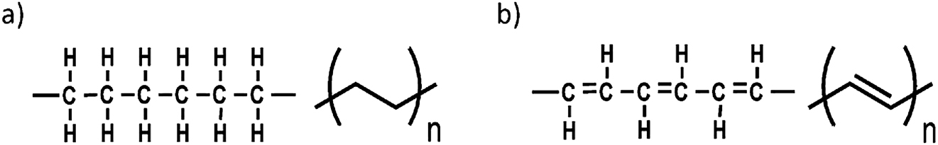
(a) Structural formula (left) and shorthand formula (right) of polyethylene; (b) Structural formula (left) and shorthand formula (right) of polyacetylene. In the shorthand formula, a carbon atom is present when two lines intersect. Hydrogen atoms are not drawn but are present to complete the four bonds that each carbon atom needs. All other atoms that are connected to carbon are shown.
Discovery of semiconducting polymers
The discovery of the first conducting polymer was accidental (Shirakawa, McDiarmid, & Heeger, 2003) but it was a profound discovery that led to the Nobel Prize in 2000 for three researchers (Heeger, 2001; MacDiarmid, 2001; Shirakawa, 2001). Polymers, such as polyethylene are synthesized from the monomer ethylene (Figure 2a), which contains a double bond. In the reaction, the double bond in the monomer is broken to form two new single bonds to allow the monomers to connect with each other. Hideki Shirakawa, a polymer chemist in Japan, was exploring the use of this chemistry to polymerize a monomer containing a triple bond. In analogy to polyethylene synthesis, one of the bonds in the monomer should break to create two new single bonds to connect the monomers, which would then result in an alternating single bond and double bond polymer known as polyacetylene (Figure 2b).
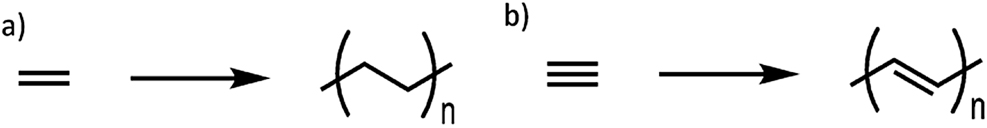
Synthetic scheme for (a) polyethylene and (b) polyacetylene.
Initially, when Shirakawa and his team of researchers tried this polymerization, they would obtain a black insoluble powder, not unlike brick dust, that they couldn’t do anything with. However, one of the researchers made a fortuitous mistake of using a thousand times more catalyst than normally is used, and this resulted in a silvery film, that looks like a metal and behaves like a metal, on the walls of the reaction vessel. Shirakawa and his collaborators Alan Heeger and Alan MacDiarmid at the University of Pennsylvania worked on this polymer further and reported the first ever organic polymer that showed levels of conductivity that were similar to that of metals (Shirakawa, Louis, MacDiarmid, Chiang, & Heeger, 1977). While this discovery may seem obvious now, at that time, to think that something that is only made of carbon and hydrogen could conduct electricity was unimaginable. This discovery has now led to a whole new area of research known as organic electronics. Related materials are being used in a wide range of applications including in OLEDs (Thejo Kalyani & Dhoble, 2012) and OSCs (Mazzio & Luscombe, 2015). A wide range of other semiconducting materials have now been discovered some of which are shown in Figure 3 (Holliday, Li, & Luscombe, 2017; Price, Stuart, Yang, Zhou, & You, 2011; Zhang et al., 2010; Zhao et al., 2016). While the structures may seem complex, they all have one thing in common which is that they are all π-conjugated systems with alternating single and double bonds along the polymer backbone.
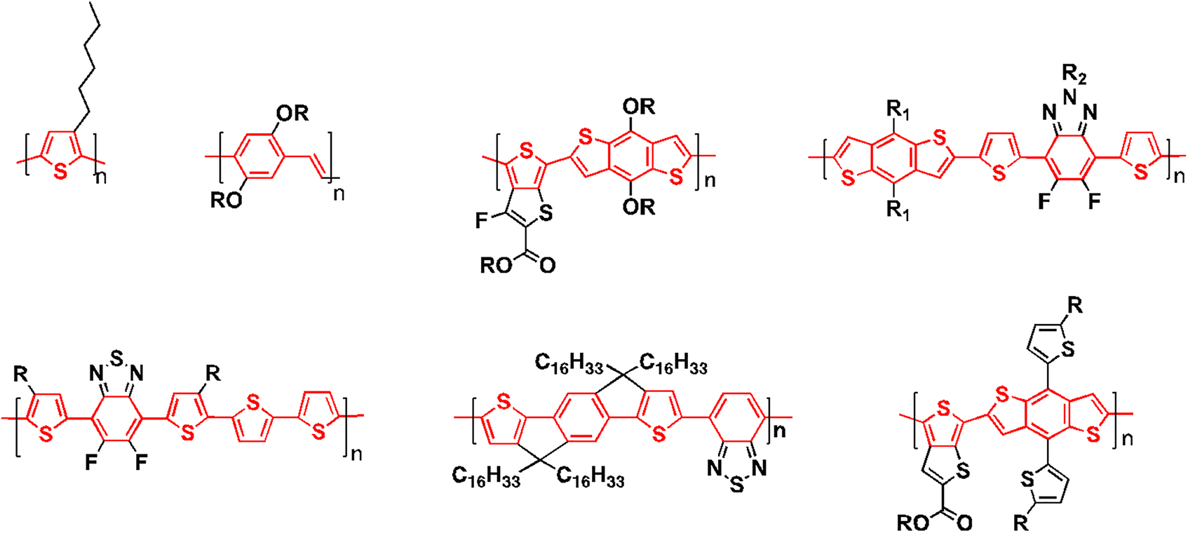
Examples of π-conjugated polymers. The π-conjugated core is highlighted in red.
How they work
Bonding in organic molecules
In order to understand why semiconducting polymers have the properties that they do, it is important to understand how bonding occurs in polymers. Most organic molecules are made up of covalent bonds. Specifically, let’s take a look at a methane molecule as an example (Figure 4a). Methane consists of one carbon (C) atom and four hydrogen (H) atoms and has the chemical formula CH4. Carbon is a group 14 element whereas hydrogen is a group 1 element in the periodic table. This means that a carbon atom has four electrons in its outer shell and a hydrogen atom has one electron in its outer shell. In order to form a C–H bond, a hydrogen atom will share its electron with carbon so the covalent bond consists of two electrons. This bond is known as a single or σ-bond. Since carbon has four electrons, it is able to form four bonds with four hydrogen atoms to create the molecule, CH4.[1] Let us now consider a molecule such as ethane, C2H6 (Figure 4b). The bonding in ethane is similar to that of methane. However, instead of each carbon atom being bonded to four hydrogen atoms, each carbon atom is bonded to three hydrogen atoms and one carbon atom. The end result is that each carbon atom has four bonds and each hydrogen atom has one bond.
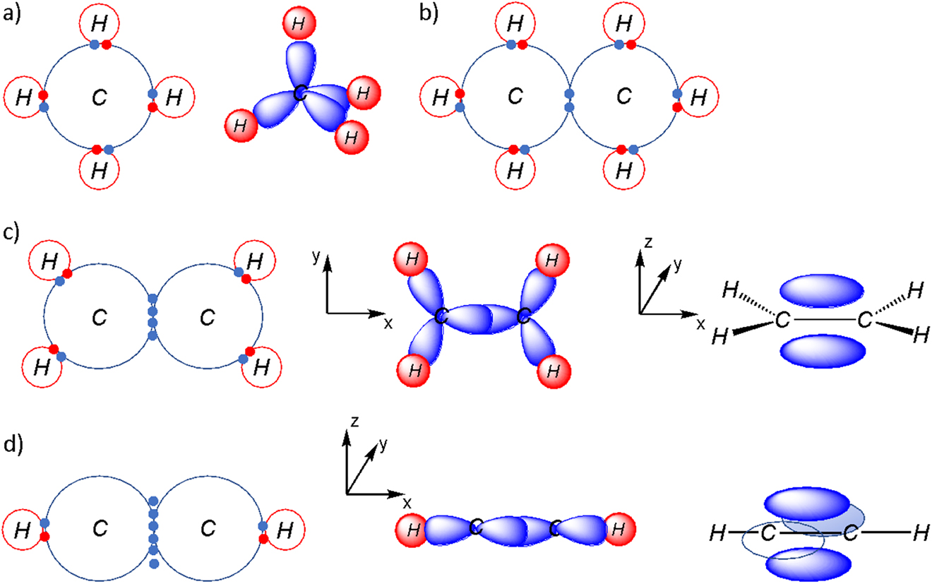
(a) Covalent bonding in methane (left) shown using Lewis structures and the σ-bonded framework (right) shown using the hybrid orbital model; (b) Covalent bonding in ethane shown using Lewis structures; (c) Covalent bonding in ethylene (left) shown using Lewis structures, σ-bonded framework (middle) shown using the hybrid orbital model, π-bond (right) shown as molecular orbitals; (d) Covalent bonding in ethyne (left) shown using Lewis structures, σ-bonded framework (middle) shown using hybrid orbital model, two π-bonds (right) shown as molecular orbitals.
The situation begins to change when we now have ethene/ethylene, C2H4 (Figure 4c). In this case, a carbon will still form a single bond with the hydrogen atoms and the other carbon atom. However, that on its own would result in carbon only have three bonds when four bonds are preferred. Instead, a π-bond (Figure 4c right) resulting from the overlap of two pz orbitals provide the fourth bond for each carbon atom. The shape of the bond, or the orbital,[2] that contains electrons begins to change. While the σ orbital lies within the plane of the molecule and lies between the two atoms, the π orbital lies above and below the plane of the molecule. Acetylene (or ethyne), C2H2 (Figure 4d), takes this one step further. Each carbon atom is only bonded to one hydrogen atom, leaving three bonds, a σ-bond and 2 π-bonds between the carbon atoms. The π-bonds result from the overlap of two pz orbitals and two py orbitals.
Bonding in polymers
Let’s now consider bonding in polymers such as polyethylene and polyacetylene. For the former, the bonding is an extension of what happens in ethane. However, instead of each carbon atom being bonded to three hydrogen atoms and one carbon atom, each carbon atom is bonded to two hydrogen atoms and two carbon atoms. The polymer consists of just single bonds with the electron density localized between atoms. These localized electrons cannot move long distances and so polyethylene is an electronically insulating material. In contrast, the bonding in polyacetylene is an extension of ethylene. If one looks at the bonding between the carbon atoms, all will have σ-bonds but every other bond will also have a π-bond. As mentioned before, the π orbital lies above and below the plane of the molecule. When there is a series of π orbitals that are spaced evenly and closely to each other, these orbitals can start to overlap allowing for delocalization of electrons. The π-conjugated structure thus allows for conductivity to be achieved.
Another unique feature about π-conjugated polymers is that they are very colorful – in other words, they are able to absorb visible light and also emit visible light. In order to understand this, we again need to look at the bonding but this time also consider the energy levels of the orbitals. Take for example the hydrogen molecule, H2. The atomic orbitals on each hydrogen overlap to form a new molecular orbital for the σ-bond. An anti-bonding molecular orbital is also formed known as σ*. This is shown in Figure 5a. The σ orbital is lower in energy than the σ* orbital. Each orbital can take two electrons and so the two electrons from each hydrogen occupy the σ orbital. In this case, the σ orbital is also known as the highest-occupied molecular orbital (HOMO) because it is the highest energy orbital that contains electrons. Conversely, the σ* orbital is known as the lowest-unoccupied molecular orbital (LUMO) because it is the lowest energy orbital that doesn’t contain electrons.
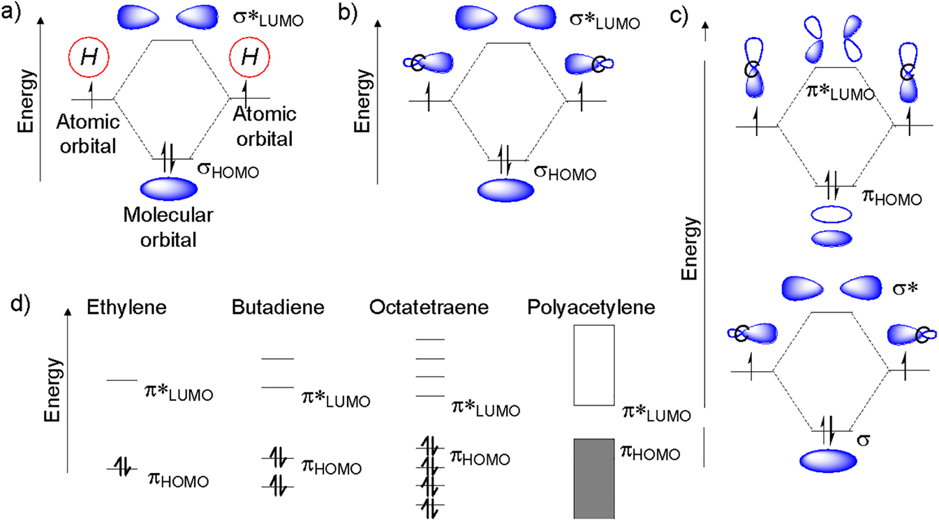
Molecular orbital energy level diagrams for (a) hydrogen; (b) ethane; (c) ethylene; (d) ethylene, butadiene, octatetraene, and polyacetylene.
Let us now reexamine ethane again but only looking at the C–C bond and not the C–H bonds. In much the same way that a σ orbital and a σ* orbital was formed for hydrogen, the same happens when the C–C bond is formed (Figure 5b). Similarly, for ethylene, a σ orbital and a σ* orbital is formed. In addition to this, a π orbital and a π* orbital is formed (Figure 5c). For ethane, the HOMO and LUMO are the σ orbital and the σ* orbital, respectively, but in ethylene, the HOMO and LUMO are the π orbital and a π* orbital, respectively. As we increase the number of double bonds in the π-conjugated molecule going from butadiene, octatetraene to eventually polyacetylene, the HOMO level increases in energy and the LUMO level decreases in energy. As a result the HOMO-LUMO energy gap decreases as the conjugation length is increased (Figure 5d).
Light absorption by organic molecules and macromolecules
When light shines on a molecule, if the energy, E, of the light, given by E = hc/λ where h is the Planck’s constant, c is the speed of light, and λ is the wavelength of light, is larger than the HOMO-LUMO energy gap, then an electron can be excited from the HOMO to the LUMO (Figure 6a). This corresponds to light absorption. After some time, the electron can relax from the LUMO to the HOMO and can result in light emission. The color of the light absorbed and emitted is related to the HOMO-LUMO energy gap. For ethylene, the HOMO-LUMO energy gap is such that the wavelength of light that is absorbed lies in the UV-region (wavelength 100–400 nm) (Figure 6b). However, for extended π-conjugated molecules, the HOMO-LUMO energy gap is small enough that this translates into visible light (wavelength 400–800 nm) being absorbed or emitted.[3] As such, the π-conjugated structure not only allows for electronic conductivity but it also allows for visible light absorption and emission, which are crucial properties for applications in OLEDs and OSCs.
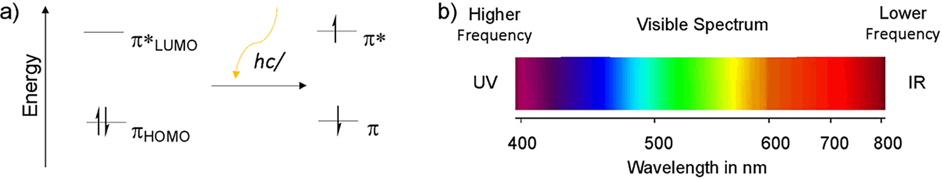
(a) Molecular orbital energy level diagrams showing photoexcitation from the HOMO to the LUMO upon light absorption; (b) Wavelength of light that corresponds to the visible spectrum.
Synthesis of polymers
Basic background information about polymer synthesis
Polymerization is the process of converting monomers into polymers. When the polymerization involves reactions between molecules of all degrees of polymerization (i.e., monomers, dimers, trimers, tetramers, oligomers, etc.), the process is known as polyaddition or polycondensation (Figure 7a). When this involves sequential addition on monomer units to an active site the process is known as chain polymerization (Figure 7b).
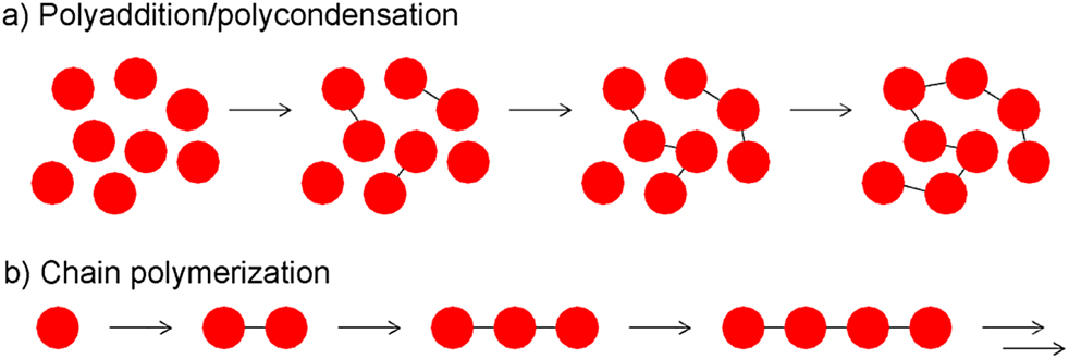
Schematic representation of (a) polyadditions/polycondensations. The difference between the two is that polyadditions result in no loss of small molecule whereas the latter involve loss of a small molecule e.g., water; (b) chain polymerizations.
In polyaddition, polymers are formed by bi- or greater functional molecules of all sizes reacting by addition reactions without evolution of low molar mass by-products during the propagation reaction. In polycondensation, polymers are formed by condensation reactions, which produce small molecule(s) during each propagation step. For these polymerizations to occur, the monomers must possess at least two reactive sites. An example of polyaddition involves the synthesis of polyurethane from a diisocyanate compound and a dialcohol compound (Figure 8a). An example of polycondensations includes the synthesis of polyesters, where a dialcohol can be reacted with an acid chloride (Figure 8b), and polyamides where a diamine can be reacted with a dicarboxylic acid (Figure 8c).
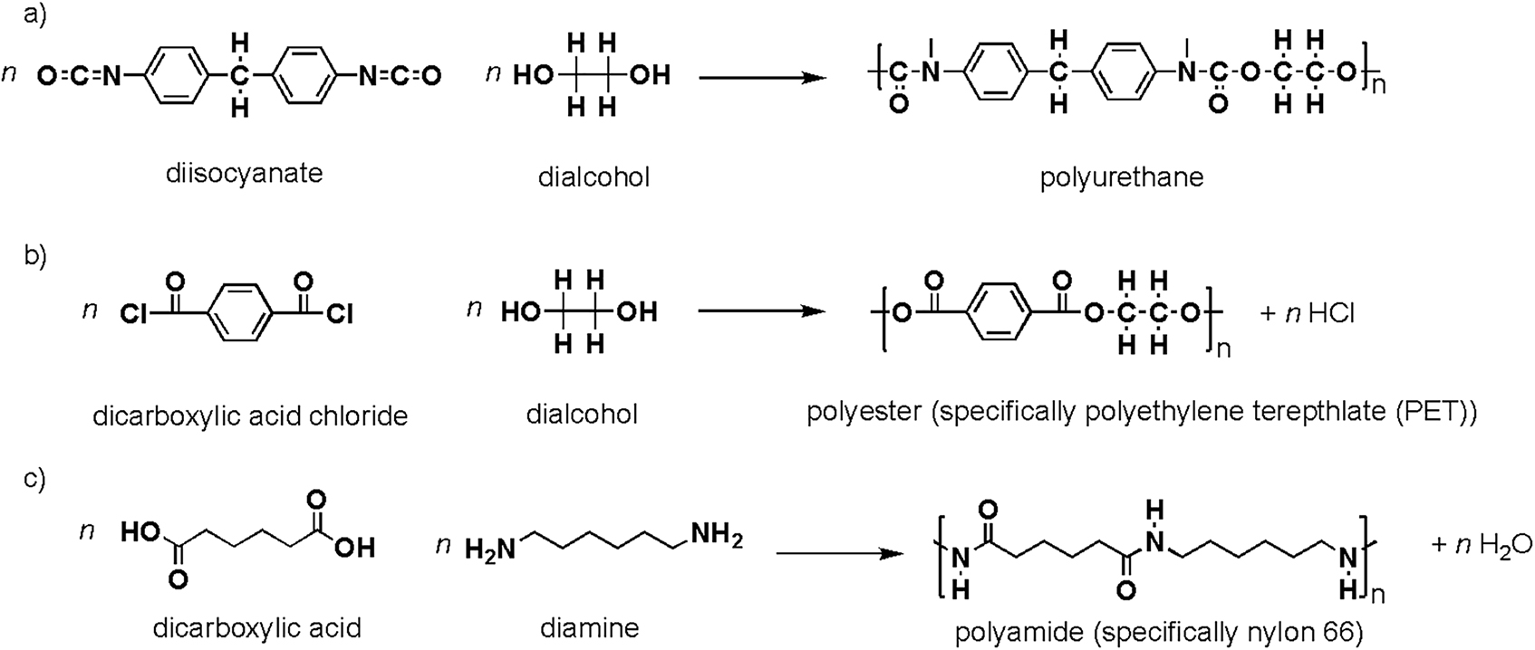
Reactions schemes for the synthesis of (a) a polyurethane; (b) a polyester, specifically polyethylene terephthalate (PET); (c) a polyamide, specifically nylon 66.
The synthesis of polyethylene or polyacetylene, as introduced in the previous section, is an example of a chain polymerization (Figure 9). Chain polymerization comprises initiation, propagation and, optionally, deactivation steps. In polyethylene or polyacetylene synthesis, an initiator reacts with the ethylene or acetylene monomer one at a time to eventually form the polymer.
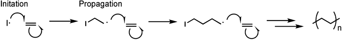
Polyethylene synthesis where I• represents the initiator radical. For polyacetylene, the ethylene monomer would be replaced with ethylene and the polymer repeat unit would contain a C=C bond instead of a C–C bond. Single-headed arrows represent the movement of single electrons.
Specifics related to semiconducting polymer synthesis
While a simple semiconducting polymer, such as polyacetylene, can be made using a chain polymerization, as shown in Figure 3, most semiconducting polymers have more complex structures. As such, most other semiconducting polymers are synthesized using polycondensation. Some of these examples are shown in Figure 10. Figure 10a shows the most common method that semiconducting polymers are synthesized (Carsten, He, Son, Xu, & Yu, 2011). In this case, one monomer functionalized with halogens (X) and a different monomer functionalized with an organometallic reagent (MX), a substance that has at least one metal to carbon bond where the carbon is part of an organic group (https://doi.org/10.1351/goldbook.O04328), is used where X cannot react with itself, and MX cannot react with itself.[4] As a result, a polymer as shown in the figure can be synthesized where Ar represents a (hetero)aromatic species.[5] In the case when a double bond is required between the (hetero)aromatic groups, a Horner-Wadsworth-Emmons reaction is commonly used (Figure 10b) (Krebs & Jørgensen, 2003). Finally, when functional groups are needed on the double bond, a Knoevenagel reaction is frequently used (Figure 10c) (Cao et al., 2019).
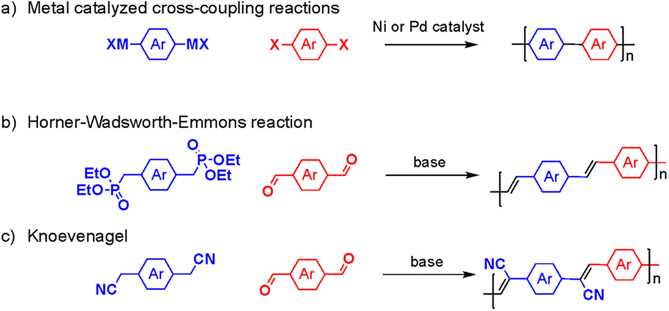
Commonly used synthetic methods for semiconducting polymers.
(a) Metal-catalyzed cross-coupling reaction; (b) Horner-Wadsworth-Emmons reaction; (c) Knoevenagel reaction.
Semiconducting polymer applications
There are a wide variety of potential applications for semiconducting polymers which can take advantage of their conductive properties (in other words, their ability to allow charges to move) or their semiconducting properties (in other words, their ability to absorb or emit light energy). When referring to charges, we will be using the terms electrons (negatively charged particles) or holes (the absence of electrons – positive charges), which are responsible for creating electric current in the semiconducting polymers. Since we are focusing on their semiconducting nature, two important applications we will examine here are applications in OSCs and OLEDs. These two applications can be considered almost as “opposite sides of the same coin” since OSCs create electricity when light is absorbed and OLEDS emit light when electricity is applied to the device. Both rely on the important, already discussed (in Figures 5 and 6) HOMO to LUMO transition either with light absorption (excitation of electron from HOMO to LUMO in OSCs – Figure 11a) or light emission (electron relaxation from LUMO back to HOMO in OLEDs – Figure 11b). It is apparent that there are also some differences in the makeup of the active layer in the OSC (Figure 11a) and the OLED (Figure 11b) which are important and will be analyzed in the upcoming sections.
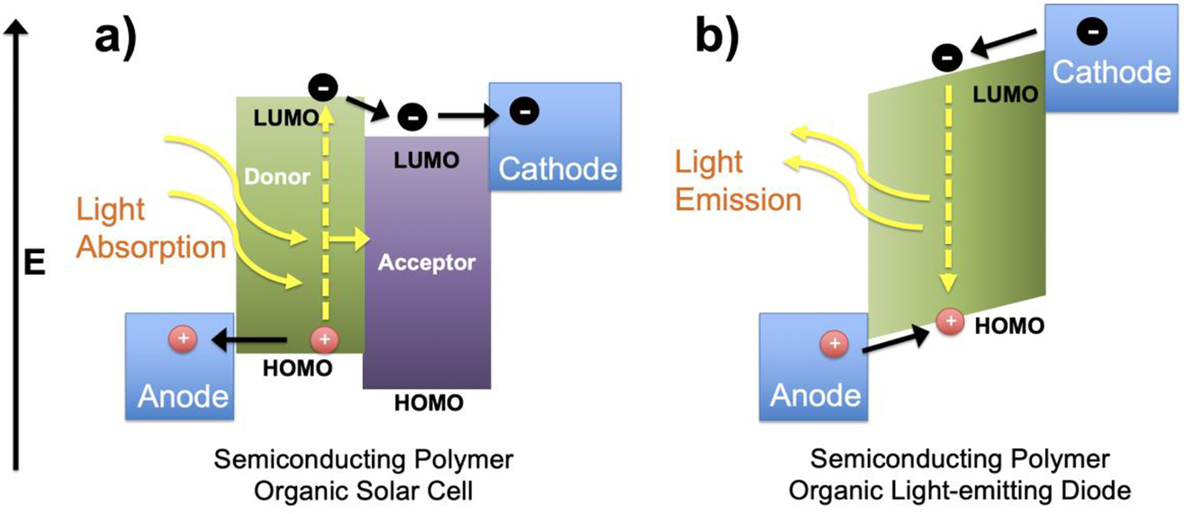
Energy level diagrams of semiconducting polymer with the movement of electrons (−) and holes (+) in an (a) organic solar cell and (b) organic light-emitting diode.
Organic electronics
These two applications (OSCs and OLEDs) fall under a larger category of the emerging field of organic electronics where molecules and polymers are being utilized to create electronic devices. This is an exciting area of technological development because it offers the ability of low-cost electronic device manufacturing on a large-scale using ink printing technologies that already exist. In addition, organic electronics such as OSCs and OLEDs can be made mechanically flexible and can be integrated into windows or building structures for unique solar energy conversion or lighting applications. OLED-based screens on smartphones have become commonplace as are large area digital screen applications utilizing this technology. The development of semiconducting polymeric materials has enabled these advancements. The following two sections will look at the basics of how OSCs and OLEDs work, and will also briefly overview two available hands-on activities that teachers can use to demonstrate how a semiconducting polymer can be turned into an OSC or OLED.
Photovoltaic devices
A photovoltaic device (or solar cell) is a device that can convert sunlight into electricity (Mazzio & Luscombe, 2015). It is common to see many solar cells (linked together to form a large solar panel) on parking meters, on rooftops, or in large arrays of panels on a solar farm. Historically, inorganic semiconductors such as silicon have been used in these types of photovoltaic cells. Silicon is an ideal semiconductor material for solar energy conversion because it is abundant, and in its purified crystalline form absorbs a large portion of the solar spectrum (the sun’s irradiation). This enables high efficiency devices to be constructed. This is important for solar cell technology because the higher the efficiency of the device, the smaller the surface area that is needed to provide the power for a building or portable application.
The drawbacks of using an inorganic semiconductor such as silicon includes the requirement of high temperature processing to access highly purified silicon and complicated device manufacturing processes. This has historically made silicon solar cells expensive to buy and install. Although, as the demand for solar energy conversion technology has increased, the cost of solar has become more competitive with non-renewable energy sources (such as oil, coal, and natural gas).
Organic polymer solar cells
After the discovery of conductive polymers, it was realized that the semiconductive nature of the polymeric material could be utilized to absorb light and potentially capture and convert that energy into electrical power. To realize this, an important achievement occurred when a group led by Alan Heeger discovered that a semiconducting polymer showed rapid photoinduced electron transfer to an allotrope of carbon called a buckminsterfullerene (Sariciftci, Smilowitz, Heeger, 1992). A buckminsterfullerene is a spherical form of carbon made up of 60 carbon atoms in the shape of a soccer ball. They are called buckminsterfullerenes (or C60) after the architect Buckminster Fuller (Figure 12a).
![Figure 12: (a) Photoinduced charge transfer observed between a semiconducting polymer poly [2-methoxy-5-(2-ethylhexyloxy)-1,4-phenylene-vinylene], (MEH-PPV) and C60, with (b) energy level diagram depicting the photoinduced charge transfer.](/document/doi/10.1515/cti-2020-0020/asset/graphic/j_cti-2020-0020_fig_012.jpg)
(a) Photoinduced charge transfer observed between a semiconducting polymer poly [2-methoxy-5-(2-ethylhexyloxy)-1,4-phenylene-vinylene], (MEH-PPV) and C60, with (b) energy level diagram depicting the photoinduced charge transfer.
The researchers discovered that if you illuminated a semiconducting polymer with light while the polymer was in close contact with the C60, a charge-transfer state could be obtained which is when an electron is donated from the semiconducting polymer to the C60 molecule (Figure 12a). This discovery then led to development of working solar cell devices based on blends of conjugated polymers with an appropriate acceptor. By choosing materials with the correct HOMO/LUMO energy levels, devices were developed that could turn this initial photoabsorption and charge transfer into a working solar cell device (converting sunlight into electrical power). And, remarkably it could all be processed at low temperatures by spin casting a thin film that contained the semiconducting polymer and the acceptor material. Spin casting is one method to create a very uniform thin film whereby a substrate is spun at a high rate while dropping a solution of the material onto its surface. Overall, this work led to a major global research effort to discover new semiconductor polymer candidates that enabled greater light absorption and more rapid charge conduction to help improve the overall solar photoconversion efficiency.
How polymer photovoltaic devices work
To make an operating semiconducting polymer solar cell device there are four processes that need to occur.
Photon or light absorbance by the semiconducting polymer (excitation from the HOMO to the LUMO energy levels)
Excited-state (also called exciton – excitation from HOMO to LUMO – Figure 6) diffusion to the donor/acceptor interface
Charge separation at this interface to create electrons (negatively charged) and holes (positively charged)
Electrons and holes are collected at separate metallic electrodes.
Step 1:
Figure 13 depicts a graphical representation of each step of the process. For these four processes to work efficiently, the device needs to be engineered to maximize each step. For step 1, the light absorption properties of the semiconducting polymer are largely controlled by the molecular structure of the polymeric material. As was mentioned in previously, the alternating single/double bond arrangement allows for the unique electronic structure of the polymer to be observed. Specifically, the decreased HOMO-LUMO energy gap described allows the semiconducting polymer to absorb visible light (Figure 6a and b), which is important for creating an efficient photovoltaic device. The solar radiation that reaches the Earth’s surface has a specific distribution of various wavelengths of light (Figure 14). It is the goal to absorb as much of the available solar energy as possible. While at the same time, the light needs to be of sufficient energy to create an electrical potential within the cell (which is generated in step 3). Lower energies of light (e.g., infrared radiation – Figure 14) are typically not useful for creating efficient photovoltaic devices.
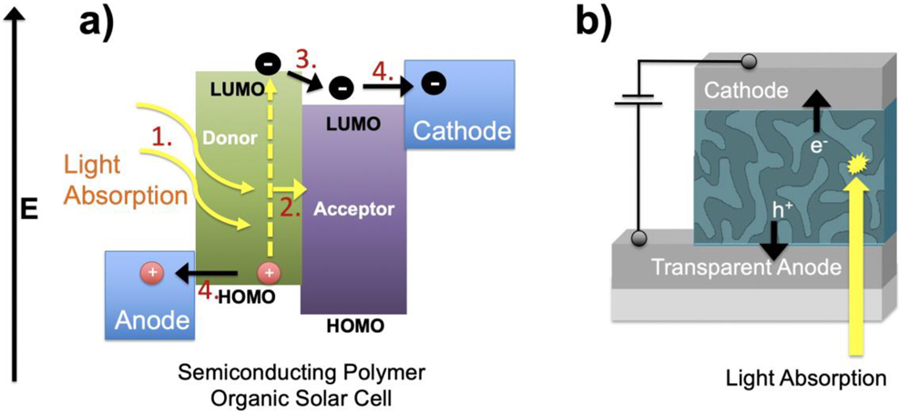
(a) Energy level diagram and device operation steps for semiconducting polymer solar cell, and (b) device structure showing metallic contacts (cathode and anode) and a bulk heterojunction light-absorbing layer.
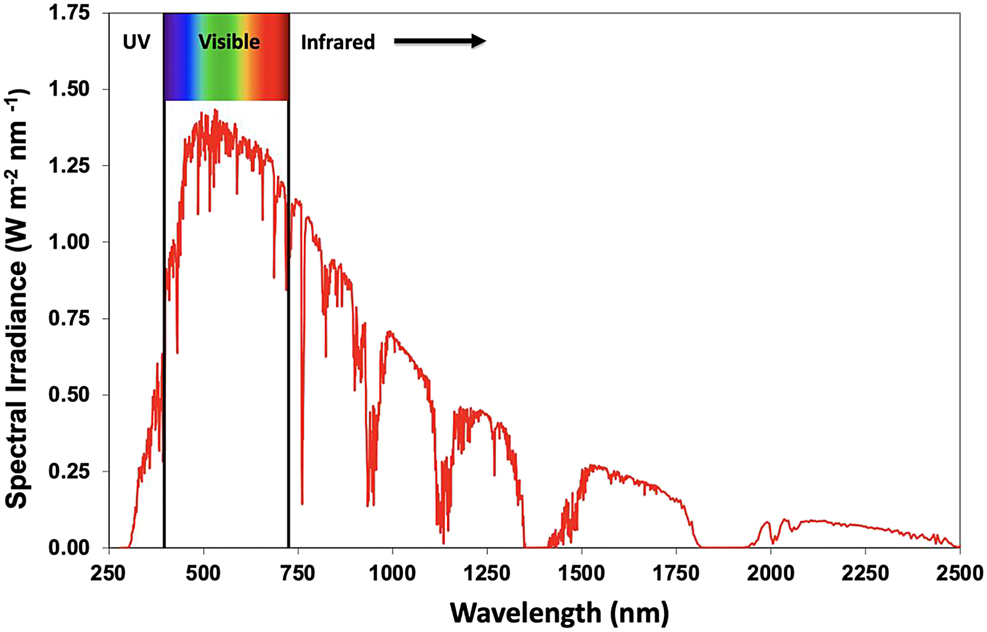
Standard Solar Radiation Spectrum at Sea Level (based upon National Renewable Energy Laboratory data). https://www.nrel.gov/grid/solar-resource/spectra.html
Step 2:
After light is absorbed, an excited-state (also called exciton – Figure 6) is formed in the material. This is created from the promotion of an electron from the HOMO into the LUMO leaving behind a positive charge or a hole (h+). This electron-hole pair is bound together electrostatically, and cannot separate unless it diffuses to an interface between the donor and acceptor material. The lifetime of this exciton is very short (∼10−9 s = nanoseconds). If the exciton doesn’t reach the interface in time, it will relax back down to the ground state and release the energy as fluorescence (emission of light – Figure 6) or heat. The mechanism of this exciton diffusion to the interface between the donor and acceptor where the electron transfer can occur is step 2 in the overall process. This is a critical step, because to generate electrical power efficiently, each exciton generated must reach the interface and be converted into electrons and holes (also called free-charge carriers). Many photons must be continuously absorbed and converted into free charge carriers (electrons and holes) to generate enough electrical current to create an efficient solar cell device.
It has been found that the exciton diffusion in most semiconducting polymers is very small (around 10 nm). Considering that the overall thickness of most organic solar cells is typically between 50 and 100 nm, most excitons would not be able to reach an interface if the device was composed of two planar layers stacked on top of one another. To overcome this challenge, researchers simply blended the donor and acceptor materials to create what is called a bulk heterojunction device (Scharber & Sariciftci, 2013). This ensures that any exciton generated does not have to travel very far to reach an interface between the donor and acceptor materials. This drastically improved the efficiency of organic semiconducting polymer solar cells. Figure 13b depicts the bulk heterojunction architecture and shows the metallic electrodes used to contact the top and bottom layer of the solar cell device. To allow light to get to the active, light absorbing layer, the bottom contact is made of a transparent conductor layer, commonly indium tin oxide (ITO), supported on a glass substrate.
Step 3 and step 4:
The last two remaining steps involve the dissociation of excitons at the interface to generate electrons and holes (step 3), and their migration back to the anode (holes) and the cathode (electrons) (step 4). The dissociation of the exciton requires that the offset between the LUMO of donor and LUMO of acceptor to be energetically greater than the binding energy of the electron-hole pair (exciton). The difference in energy between the HOMO of the donor and LUMO of acceptor is generally considered to be the maximum attainable voltage the device can generate, although there is a myriad of additional electron/hole processes that tend to lower this observed value.
The semiconducting polymer materials need to have efficient hole (or electron) conducting properties to allow for the free charge carriers to be collected. In addition, the energy levels of metal electrode contacts (anode and cathode) help to encourage electron and hole migration away for the bulk heterojunction and collection (Figure 13a). The overall actions of the electron/hole generation and migration help to generate the observed potential (solar cell voltage) and the current density (speed of the electrons in the cell per illuminated area). The voltage (V with units V) multiplied by the current density (J with units mA cm−2) gives us the electrical power output of the solar cell.
Organic light-emitting diodes (OLEDs)
OLED research and development are a rapidly growing technology (Mentley, 2002). OLEDs can now be found in digital screens in TVs, touch screen displays in mobile phones/tablets, cameras, and many similar display applications. The advantages of using OLED screens include their lightweight, flexible screens that have good viewing angles and low power consumption compared to previous generations of digital displays. One reason that OLEDs use less energy is that the materials used in the displays emit light directly and require no backlighting.
OLED emission mechanism
The mechanism for which an applied electrical potential can produce light emission is referred to as electroluminescence. There are several electron-hole recombination pathways for which light emission can be produced through the application of a voltage to an OLED device. For simplicity, we will focus on a general mechanism first outlined in Figure 11b (Thejo Kalyani & Dhoble, 2012). Similar to an OSC device, and OLED is made using semiconducting molecules (or polymers) deposited as a very thin film (<100 nm) onto a conductive surface requiring one of the conductors to be transparent to allow light emission to be observed. Also, similar to the OSC device, we can split the overall mechanism into four steps however you will see that the order of the steps is reversed (Figure 15a).
Injection of electrons and holes into the organic semiconductor layer
Charge transport of electrons and holes
Exciton (electron-hole) formation in the emitting layer
Electron-hole combination producing emission of light
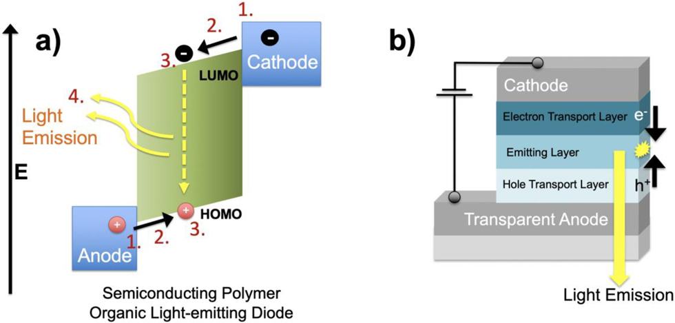
(a) Energy level diagram and steps for light emission of OLED device, and (b) device structure showing metallic contacts (cathode and anode), hole and electron transport layers, and light-emitting layer.
This conversion of electricity into light emission is somewhat simplified compared to the OSC device requiring only a single light emissive organic layer structured between the two metallic contacts. In practice however, often there are additional organic layers that provide better electron and hole transport to the emitting layer, and blocking layers to ensure that electrons and holes only combine together in the light emissive layer (Figure 15b). These efforts help to improve the light emission efficiency of the device.
OLED colors
The mechanism for generating the light emission involves the application of a voltage to the device with sufficient energy to inject electrons and holes into the organic (or polymeric) active layer. The intensity and brightness of the generated light depends on the efficiency of this process in addition to how much power is being applied to the device. The more voltage applied and current moving through the device, the more electrons holes will combine and emit light.
The color (wavelength of light emission) from the organic layer is due to the HOMO-LUMO gap of the semiconducting organic polymer. This gap is dependent upon both the p-orbital (conjugation) structural features of the molecule or polymer, and also various functional groups that can fine-tune the energies of the HOMO and LUMO orbitals making the energy gap larger or smaller (Figure 5). For instance, if the conjugated polymer MEH-PPV which has an energy gap of ∼2.0 eV, where 1 eV = 96.5 kJ/mol, is used as the emissive layer in an OLED device, we would expect that it emits yellow-orange light (emission 620 nm – Figure 6b). This polymer can be used to demonstrate a working OLED device using a conjugated polymer (in the following section).
Hands-on activities
Organic semiconducting polymer solar cell and organic light-emitting diode
A simple, hands-on semiconducting polymer activity that can be done at the high school or secondary education level has been previously reported (Enlow, Marin, & Walter, 2017). A brief overview of this activity which makes use of the same semiconducting polymer (MEH-PPV, Figure 17a) for both activities is described below.
Organic semiconducting polymer solar cell
To demonstrate the photovoltaic effect of a semiconducting polymer, a simple device can be constructed using MEH-PPV and a cheap inorganic nanocrystalline material (titanium dioxide – TiO2). A solution TiO2 nanoparticles are deposited onto a transparent conductive glass electrode and heated to form a highly porous electrode. Then a solution of MEH-PPV dissolved in chloroform is drop cast onto the electrode and allowed to dry. The MEH-PPV and nano-porous TiO2 electrode form a bulk heterojunction light absorbing layer. The sandwich-type solar cell is completed with an electrolyte solution (I−/I3−) to contact the polymer layer. Figure 16a and b depicts an energy level diagram with electron movement of an operating solar cell device and a digital image of the completed device.
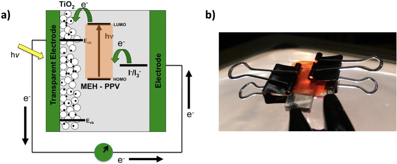
(a) Energy level diagram of an operating MEH-PPV/TiO2 solar cell with device cross-section and (b) image of the completed device. (Note: FTO is transparent conductive electrode) Reprinted with permission from (Enlow, Marin, & Walter, 2017). Copyright 2017 American Chemical Society.
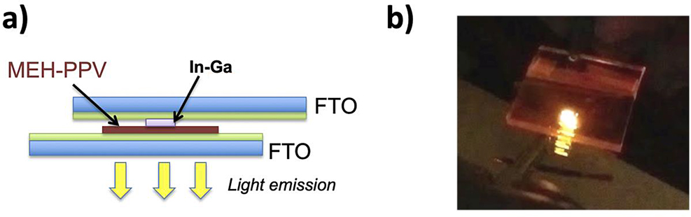
(a) OLED device cross-section, and (b) image of polymer OLED emission. Reprinted with permission from (Enlow, Marin, & Walter, 2017). Copyright 2017 American Chemical Society.
In this device, the MEH-PPV polymer functions as the light absorber and donor material, whereas the TiO2 (whose energy gap is too large to absorb visible light) acts as the acceptor and electron-transport material. Illumination of the device induces photoexcitation of the MEH-PPV followed by electron donation to the TiO2 layer (Figure 16a). The electrolyte solution provides an electron back to the dye completing the device circuit. An assembled device can be illuminated outside with sunlight or with a white light resulting in the generation of a photovoltage and photocurrent which can be measured with an electrical multimeter. Two alligator clip wire leads are used to contact the FTO (fluorine-doped tin oxide) transparent conductive electrodes for measuring the power output (Figure 16b).
Semiconducting polymer organic light-emitting diode
The same conjugated polymer (MEH-PPV) can also be used to demonstrate electroluminescence which is observed in OLED devices. In this simple device, a thin layer of MEH-PPV is cast from a chloroform solution onto an FTO electrode. This polymer can then be contacted with a graphite rod or a liquid metal indium-gallium contact. An additional FTO electrode is placed on top to complete the device, and a voltage is applied from a 9 V battery which causes the polymer OLED device to emit light. Figure 17a depicts a cross-section of the device construction and Figure 17b shows an image of the polymer OLED device emitting yellow light.
More information about these hands-on activities including resources for preparing teachers to demonstrate or teach these activities, and information about where to obtain the materials needed can be found in the previously reported work (Enlow et al., 2017) or by contacting the corresponding author (M. Walter) of this article. Instructors will find these activities very exciting and informative for students about contemporary polymer activities with real-world applications.
Conclusions
In this paper, we sought to provide a tutorial for upper secondary students about organic semiconducting polymers. The paper covers their discovery, how they work, how they can be synthesized, and two examples of their applications. Lastly, two hands-on semiconducting polymer activities have been presented that enable educators to demonstrate these two important polymer semiconducting applications (OSCs and OLEDs). Both activities enable students to construct actual working devices using solution-processable semiconductor polymer materials. Overall, we hope that educators will find that the introduction to semiconducting polymers, their syntheses and properties, and their real-world applications can inspire the next generation of science, technology, engineering, and mathematics students.
Funding source: International Union of Pure and Applied Chemistry
Award Identifier / Grant number: 2019-035-1-050
Acknowledgments
Support from IUPAC is gratefully acknowledged.
Author contributions: All the authors have accepted responsibility for the entire content of this submitted manuscript and approved submission.
Research funding: This work was supported by IUPAC Project no. 2019-035-1-050 (Polymer Division (Division IV) and Committee on Chemistry Education).
Conflict of interest statement: The authors declare no conflicts of interest regarding this article.
References
Amjadi, M., Kyung, K.-U., Park, I., & Sitti, M. (2016). Stretchable, skin-mountable, and wearable strain sensors and their potential applications: A review. Advanced Functional Materials, 26(11), 1678–1698. https://doi.org/10.1002/adfm.201504755.Suche in Google Scholar
Cao, X., Li, Y., Liu, B., Gao, A., Cao, J., Yu, Y., & Hei, X. (2019). A fluorescent conjugated polymer photocatalyst based on Knoevenagel polycondensation for hydrogen production. New Journal of Chemistry, 43(18), 7093–7098. https://doi.org/10.1039/c9nj01686d.Suche in Google Scholar
Carsten, B., He, F., Son, H. J., Xu, T., & Yu, L. (2011). Stille polycondensation for synthesis of functional materials. Chemical Reviews, 111(3), 1493–1528. https://doi.org/10.1021/cr100320w.Suche in Google Scholar PubMed
Chen, H. W., Lee, J. H., Lin, B. Y., Chen, S., & Wu, S. T. (2018). Liquid crystal display and organic light-emitting diode display: Present status and future perspectives. Light: Science and Applications, 7, 17168. https://doi.org/10.1038/lsa.2017.168.Suche in Google Scholar PubMed PubMed Central
Enlow, J. L., Marin, D. M., & Walter, M. G. (2017). Using polymer semiconductors and a 3-in-1 plastic electronics STEM education kit to engage students in hands-on polymer inquiry activities. Journal of Chemical Education, 94(11), 1714–1720. https://doi.org/10.1021/acs.jchemed.7b00332.Suche in Google Scholar
Heeger, A. J. (2001). Semiconducting and metallic polymers: The fourth generation of polymeric materials (nobel lecture). Journal of Physical Chemistry B, 105(36), 8475–8491. https://doi.org/10.1021/jp011611w.Suche in Google Scholar
Holliday, S., Li, Y., & Luscombe, C. K. (2017). Recent advances in high performance donor-acceptor polymers for organic photovoltaics. Progress in Polymer Science, 70. https://doi.org/10.1016/j.progpolymsci.2017.03.003.Suche in Google Scholar
Krebs, F. C., & Jørgensen, M. (2003). High carrier mobility in a series of new semiconducting PPV-type polymers. Macromolecules, 36(12), 4374–4384. https://doi.org/10.1021/ma025893p.Suche in Google Scholar
MacDiarmid, A. G. (2001). “Synthetic metals”: A novel role for organic polymers (Nobel lecture). Synthetic Metals, 125(1), 11–22. https://doi.org/10.1016/S0379-6779(01)00508-2.Suche in Google Scholar
Mazzio, K. A., & Luscombe, C. K. (2015). The future of organic photovoltaics. Chemical Society Reviews, 44(1). https://doi.org/10.1039/c4cs00227j.Suche in Google Scholar PubMed
Mentley, D. E. (2002). State of flat-panel display technology and future trends. In Proceedings of the IEEE. Vol. 90 (pp. 453–459). IEEE. https://doi.org/10.1109/JPROC.2002.1002520.Suche in Google Scholar
Oh, J. Y., & Bao, Z. (2019). Second skin enabled by advanced electronics. Advanced Science, 6(11), 1900186. https://doi.org/10.1002/advs.201900186.Suche in Google Scholar PubMed PubMed Central
Phan, S., & Luscombe, C. K. (2019). Recent advances in the green, sustainable synthesis of semiconducting polymers. Trends in Chemistry, 1(7), 670–681.https://doi.org/10.1016/j.trechm.2019.08.002.Suche in Google Scholar
Price, S. C., Stuart, A. C., Yang, L., Zhou, H., & You, W. (2011). Fluorine substituted conjugated polymer of medium band gap yields 7% efficiency in polymer-fullerene solar cells. Journal of the American Chemical Society, 133(12), 4625–4631. https://doi.org/10.1021/ja1112595.Suche in Google Scholar PubMed
Sariciftci, N. S., Smilowitz, L., Heeger, A. J., & Wudl, F. (1992). Photoinduced electron transfer from a conducting polymer to buckminsterfullerene. Science, 258(5066), 1474–1476. https://doi.org/10.1126/science.258.5087.1474.Suche in Google Scholar PubMed
Scharber, M. C., & Sariciftci, N. S. (2013). Efficiency of bulk-heterojunction organic solar cells. Progress in Polymer Science, 38(12), 1929–1940. https://doi.org/10.1016/j.progpolymsci.2013.05.001.Suche in Google Scholar PubMed PubMed Central
Shirakawa, H. (2001). The discovery of polyacetylene film: The dawning of an era of conducting polymers (Nobel lecture). Current Applied Physics, 1(4–5), 281–286. https://doi.org/10.1016/S1567-1739(01)00052-9.Suche in Google Scholar
Shirakawa, H., Louis, E. J., MacDiarmid, A. G., Chiang, C. K., & Heeger, A. J. (1977). Synthesis of electrically conducting organic polymers: Halogen derivatives of polyacetylene, (CH) x. Journal of the Chemical Society, Chemical Communications, (16), 578. https://doi.org/10.1039/c39770000578.Suche in Google Scholar
Shirakawa, H., McDiarmid, A., & Heeger, A. (2003). Focus article: Twenty-five years of conducting polymers. Chemical Communications, (1), 1–4. https://doi.org/10.1039/b210718j.Suche in Google Scholar
Thejo Kalyani, N., & Dhoble, S. J. (2012). Organic light emitting diodes: Energy saving lighting technology – A review. Renewable and Sustainable Energy Reviews, 16(5), 2696–2723. https://doi.org/10.1016/j.rser.2012.02.021.Suche in Google Scholar
Van Den Brand, J., De Kok, M., Koetse, M., Cauwe, M., Verplancke, R., Bossuyt, F.,… Vanfleteren, J. (2015). Flexible and stretchable electronics for wearable health devices. Solid-State Electronics, 113, 116–120. https://doi.org/10.1016/j.sse.2015.05.024.Suche in Google Scholar
Zhang, W., Smith, J., Watkins, S. E., Gysel, R., McGehee, M., Salleo, A.,…McCulloch, I. (2010). Indacenodithiophene semiconducting polymers for high-performance, air-stable transistors. Journal of the American Chemical Society, 132(33), 11437–11439. https://doi.org/10.1021/ja1049324.Suche in Google Scholar PubMed
Zhao, J., Li, Y., Yang, G., Jiang, K., Lin, H., Ade, H.,…Yan, H. (2016). Efficient organic solar cells processed from hydrocarbon solvents. Nature Energy, 1(2), 15027. https://doi.org/10.1038/nenergy.2015.27.Suche in Google Scholar
© 2021 Christine K. Luscombe et al., published by De Gruyter, Berlin/Boston
This work is licensed under the Creative Commons Attribution 4.0 International License.
Artikel in diesem Heft
- Frontmatter
- Preface
- Special issue of Chemistry Teacher International in Polymer Sciences
- Review Articles
- Fundamentals of reversible addition–fragmentation chain transfer (RAFT)
- Reversible-Deactivation Radical Polymerisation: chain polymerisation made simple
- Ring-opening polymerization
- Other
- Thermal analysis: basic concept of differential scanning calorimetry and thermogravimetry for beginners
- Review Article
- Size-exclusion chromatography as a useful tool for the assessment of polymer quality and determination of macromolecular properties
- Other
- Basics of teaching electrochemical impedance spectroscopy of electrolytes for ion-rechargeable batteries – part 1: a good practice on estimation of bulk resistance of solid polymer electrolytes
- Special Issue Paper
- Basics of teaching electrochemical impedance spectroscopy of electrolytes for ion-rechargeable batteries – part 2: dielectric response of (non-) polymer electrolytes
- Good Practice Report
- Chirality analysis of helical polymers
- Other
- Fabrication and function of polymer membranes
- Review Article
- Nano- and microgels: a review for educators
- Other
- Theoretical background on semiconducting polymers and their applications to OSCs and OLEDs
- Good Practice Report
- An understandable approach to the temperature dependence of electric properties of polymer-filler composites using elementary quantum mechanics
- Review Article
- Polymer degradation: a short review