
Second-order topological phases in C 4v -symmetric photonic crystals beyond the two-dimensional Su-Schrieffer–Heeger model
-
Yafeng Chen
 and
Jie Zhu
and
Jie Zhu


Abstract
Second-order photonic topological insulators (SPTIs) with topologically protected corner states provide a unique platform for realizing the robust manipulation of light in lower dimensions. Previous SPTIs proposed in C 4v -symmetric lattices are mainly based on the two-dimensional (2D) Su-Schrieffer–Heeger (SSH) model consisting of an even number of sites in the unit cell. Moreover, second-order topological phases within high-order band gaps are rarely explored. Here, we propose a new principle of SPTIs beyond the 2D SSH model, which is realized in C 4v-symmetric lattices consisting of an odd number of sites in the unit cell. The midgap-gap-ratios of these odd-order band gaps, from the first-order to the nineteenth-order with step of two-order, are maximized by the method of topology optimization. Second-order topological phases are successfully created within these sizeable band gaps and highly localized corner states are observed. Our work offers a new route for exploring high-order topological states in photonics and other classical systems.
1 Introduction
Photonic topological insulators (PTIs), featured with topologically protected edge states that are immune to defects, offer unique ways for realizing robust light transport [1], [2], [3], [4], [5]. Obeying the conventional bulk-boundary correspondence, kaleidoscopic versions of PTIs have been realized based on various physical mechanisms, e.g., quantum Hall effect [6, 7], quantum spin Hall effect [8], [9], [10] and quantum valley Hall effect [11], [12], [13], [14], [15], [16], [17], [18], [19]. Recently, quantized electric multipole insulators [20] and second-order photonic topological insulators (SPTIs) with unconventional bulk-boundary correspondence have been proposed [21, 22]. Different from conventional PTIs with gapless edge states, SPTIs support gapped edge states and topologically protected in-gap corner states, thus providing new ways to realize robust manipulation of light in lower dimensions. By virtue of tightly localized corner states that are immune to defects, SPTIs have found promising applications in topological cavities [23, 24], topological lasers [25] and nonlinear optics [26, 27].
Crystalline symmetry plays a pivotal role in the underlying physics of SPTIs [28]. Hitherto, the main recipe of SPTIs is based on the method of shrunken/expanded unit cell, which has been studied in lattices with different symmetries, such as, kagome lattice with C 3v symmetry [29], hexagonal lattice with C 6v and C 3 symmetries [30], [31], [32], [33], and square lattice with C 4v symmetry [34], [35], [36], [37], [38], [39], among which square lattice has attracted great intentions as it expands the design space beyond traditional graphene-like structures. The study of corner states in PCs up to now has mainly considered the 2D SSH model [40] in square lattice, which has four bands in the tight-binding description, and the band gap covering all the four bands is trivial for both choices of the unit cell, thus cannot be used to support corner states (note one typically uses the band gap between the first and second bands of the 2D square SSH model to engineer corner states, which limits the size of the corresponding band gap). In this work, we propose PCs with odd-order band gaps (i.e., the number of bands below the corresponding band gap is odd, which is also equal to the number of lattice sites within the unit cell in the tight-biding description) and demonstrate the nontrivial topological features of these odd-order band gaps, which can be made very large to support more localized corner states for practical applications. We would like to note that translating the unit cell of a PC with an even-order band gap by (a/2, a/2) could not change its topological property, thus highlighting the unique features of these PCs with odd-order band gaps. Our work offers a general guidance for exploring second-order topological phases within sizeable odd-order band gaps.
2 Results and discussions
We consider PCs in 2D square lattices that respect the C 4v point group symmetry. The PCs are made of silicon with permittivity of ε = 12. Here, we mainly focus on the transverse magnetic (TM) modes while the transverse electric modes can be analyzed similarly. For convenience of discussion, in the following, frequency is normalized with respect to ωa/2πc, where ω is the angular frequency, a the lattice constant, and c the speed of light. We firstly maximize the odd-order bandgaps (from the first-order to the nineteenth-order) by the method of topology optimization (for details of the optimization method, see Appendix A). Figure 1 shows the optimized PCs (3 × 3 unit cells) with the primitive unit cells denoted by the black dashed boxes, from which one can see that the dielectric materials form isolated dielectric pillars (denoted by blue color) in the optimized PCs. Within the unit cell, the dielectric materials at the internal domain, boundaries and corners of the unit cell form intact pillars, half-pillars, and quarter-pillars, respectively. In practical applications, the pillars, half-pillars, and quarter-pillars can be simplified as cylinders, half-cylinders, and quarter-cylinders, respectively, which can be fabricated by the method of nanoimprint lithography [41]. The number of pillars n p within a unit cell can be calculated by n p = n i + n b/2 + n c/4, where n i, n b and n c denote the number of pillars at the internal domain, boundaries and corners of the unit cell, respectively. Accordingly, we find that the number of pillars within a unit cell equals to the number of bands below the band gap, which we refer to as the order of the band gap. Note that the number of pillars within a unit cell is odd for all the optimized PCs, which is distinct to the traditional PCs for SPTIs based on the 2D SSH model [34], [35], [36], [37], whose unit cell has an even number of pillars. The band diagrams of the optimized PCs calculated using COMSOL Multiphysics are presented in Figure 2, where the midgap-gap-ratios of the ten optimized PCs are 39.2%, 36.51%, 31.78%, 45.64%, 39.61%, 43.78%, 43.69%, 41.35%, 37.68% and 31.97%, respectively. These extra-wide band gaps significantly exceed those of PCs from the 2D SSH model [34], [35], [36], [37], thus are beneficial to produce more localized edge and corner states. Previous SPTIs mimicking the 2D SSH model indicate that selecting unit cells from the PCs in distinct ways could lead to different topology properties [34], [35], [36], [37]. While our PCs are not based on the 2D SSH model, it is a nontrivial question whether the optimized PCs and these extra-wide band gaps will show any topological properties. To investigate the topological properties of these sizeable odd-order band gaps of the optimized PCs, we choose two different unit cells (UCnA and UCnB, here n is the order of the band gap) from the same optimized PC, where UCnA denotes the primitive unit cell of the optimized PC (black dashed box) while UCnB (red dashed box) is obtained through translating UCnA by (a/2, a/2). As UCnA and UCnB encode the same PC, they share the same band diagram. However, the mode shape at high symmetry points (X and Γ) of the first Brillouin zone for each band could be different, which could result in different topology properties between UCnA and UCnB. The topology properties of UCnA and UCnB could be determined via the 2D polarization P = (P x , P y ), defined by [29],
in which i = x, y denotes the direction and P
x
= P
y
as the PCs respect the C
4v
point group symmetry. η
n
denotes the parity of the high symmetry points (X and Γ) for the nth band, which could be determined by the eigenmode profile (the s and d modes have an even parity (+), whereas the p mode has an odd parity (−)). The summation over n is for all the bands below the band gap. The detailed parity information for all UCnAs and UCnBs is given in Appendix B. Putting these parities into Eq. (1), we can derive that all UCnAs are topological trivial, whereas all UCnBs are topological nontrivial. Interestingly, by calculating the number of pillars n
e
at one edge of the unit cells (

Optimized PCs hosting different odd-order band gaps: (a) the first-order; (b) the third-order; (c) the fifth-order; (d) the seventh-order; (e) the ninth-order; (f) the eleventh-order; (g) the thirteenth-order; (h) the fifteenth-order; (i) the seventeenth-order; (j) the nineteenth-order. The black dashed box denotes the UCnA and the red dashed box denotes the UCnB.
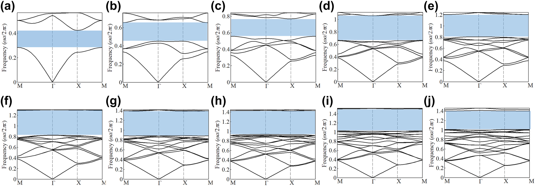
The band diagrams of the optimized PCs hosting different odd-order band gaps (shaded by light-blue regions): (a) the first-order; (b) the third-order; (c) the fifth-order; (d) the seventh-order; (e) the ninth-order; (f) the eleventh-order; (g) the thirteenth-order; (h) the fifteenth-order; (i) the seventeenth-order; (j) the nineteenth-order.
Accordingly, the corner charges are 0 for UCnAs and 1 for UCnBs, which predicts the existence of topological corner states at the corner formed between UCnAs and UCnBs. Note that our numerical experiences indicate that translating the unit cell of PC with even-order band gap by (a/2, a/2) could not change its topological property. Therefore, we only focus on exploring second-order topological phases with odd-order band gaps in this paper. To capture the key topological features of the optimized PCs in a transparent way, we construct simple tight-binding lattice models based on the configurations of UCnAs and UCnBs, as given in Appendix C.
To verify the topological edge states, the ribbon structure consisting of 6 UCnAs and 6 UCnBs with an interface between them is built, as sketched in Figure 3(a). Figure 4 shows the calculated projected band diagrams of the ribbon structures made of PCs with different orders of band gaps, and we can see that edge states appear within the bulk band gaps for all the ribbon structures. Importantly, these edge states are gapped, satisfying the prerequisites to produce corner states. The eigenfield distributions of these edge states are given in Appendix D.
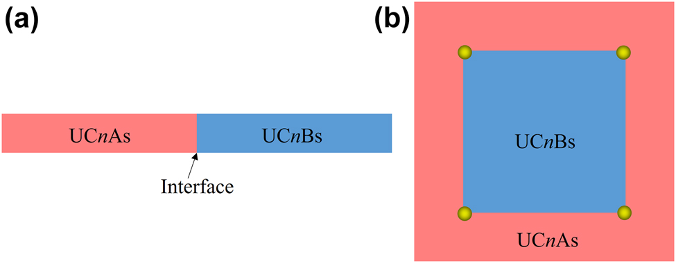
Sketchs of the supercell and the metastructure for the calculation of (a) Topological edge states and (b) Topological corner states.
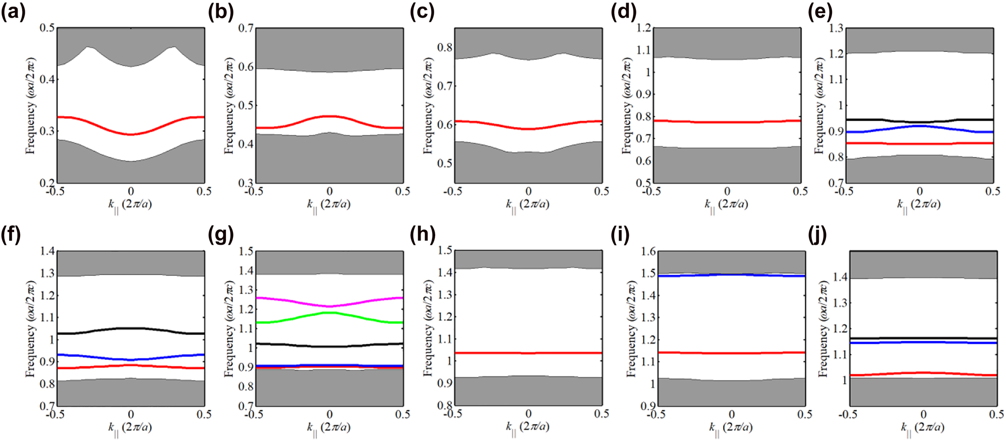
The projected band diagrams of the supercells consisting of (a) UC1A and UC1B, (b) UC3A and UC3B, (c) UC5A and UC5B, (d) UC7A and UC7B, (e) UC9A and UC9B, (f) UC11A and UC11B, (g) UC13A and UC13B, (h) UC15A and UC15B, (i) UC17A and UC17B, and (j) UC19A and UC19B.
To confirm topological corner states, we construct the metastructure consisting of 10 × 10UCnBs surrounded by 3 layers of UCnAs, as sketched in Figure 3(b). As a result, the metastructure comprises four corners that can host corner states, as denoted by the yellow balls. We label the metastructure consisting of the optimized PCs with the nth-order band gap as MSn. Figure 5 shows the calculated eigenfrequencies of MS1-MS19 by using COMSOL Multiphysics. It reveals that MS1, MS3, MS5, MS7, and MS17 host one batch of corner states consisting of four degenerated corner states. However, distinct from current SPTIs mimicking the 2D SSH model, the remaining MSs support multiple batches of corner states, thus providing possibilities for designing novel multiband photonic devices based on corner states. We would like to note that the topological invariant (i.e., Eq. (2)) of the current systems is a binary number (0 or 1) and as such it can only indicate the topologically trivial or nontrivial nature of the band gap, but cannot be used to determine the number of corresponding edge or corner states, which in general depends on the specific details (e.g., shape of the corner [45, 46] or parameters [47]) of the underlying PCs. Figure 6 presents the eigenmodes of corner states labeled by Cn in Figure 5. We can see that all corner states are indeed localized at the corners of the MSs. Moreover, the wide band gaps resulted from topology optimization enable more localized corner states. To quantitatively compare the localization degree of corner states in Figure 5 with that of corner states based on the 2D SSH model in Reference [35] (labeled by C
SSH), we further compute their mode volumes [48], defined by
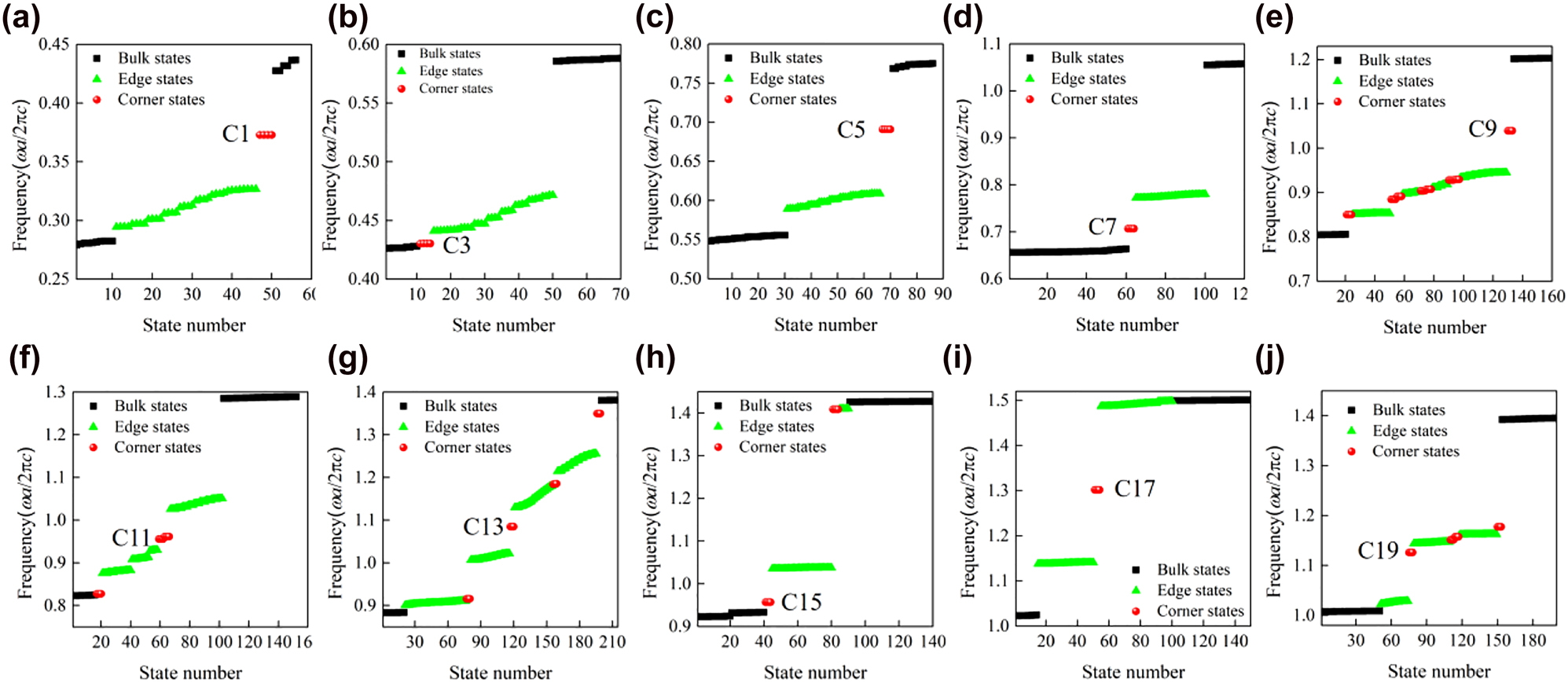
Calculated eigenfrequencies of (a) MS1, (b) MS3, (c) MS5, (d) MS7, (e) MS9, (f) MS11, (g) MS13, (h) MS15, (i) MS17, and (j) MS19. MSn represents that the metastructure is made of UCnA and UCnB.
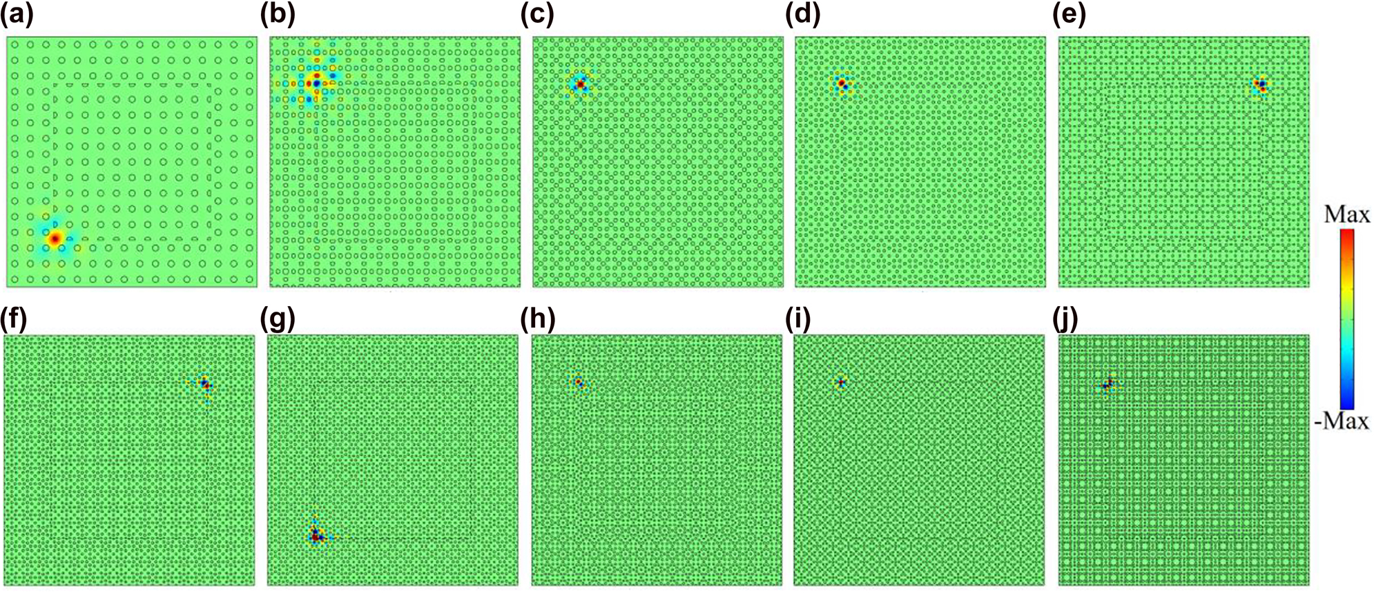
Eigenfield distributions of one representative corner state labelled by Cn in Figure 5. (a) C1, (b) C3, (c) C5, (d) C7, (e) C9, (f) C11, (g) C13, (h) C15, (i) C17, and (j) C19.
Mode volumes and Q factors of C 1–C 19 and C SSH.
| C SSH | C 1 | C 3 | C 5 | C 7 | C 9 | C 11 | C 13 | C 15 | C 17 | C 19 | |
|---|---|---|---|---|---|---|---|---|---|---|---|
| V m | 0.482 | 0.061 | 0.223 | 0.021 | 0.029 | 0.012 | 0.020 | 0.025 | 0.019 | 0.006 | 0.023 |
| Q factor | 2.6 × 10² | 3.9 × 10³ | 3.8 × 10² | 2.3 × 10⁶ | 2.3 × 10⁶ | 9.4 × 10¹⁰ | 1.6 × 10¹¹ | 1.8 × 10¹² | 2.2 × 10⁷ | 2.5 × 10¹³ | 8.8 × 10¹⁰ |
3 Conclusions
In summary, we propose a series of SPTIs hosting sizeable odd-order band gaps in C 4v -symmetric PCs beyond the widely used 2D SSH model. The relative sizes of these odd-order band gaps, from the first-order to the nineteenth-order, of the PCs are maximized by the method of topology optimization. The optimized PCs consist of an odd number of pillars in the unit cell and their band gaps significantly exceed those of PCs based on the 2D SSH model. We demonstrated that second-order topological corner states exist within these band gaps, which are more localized than those based on the 2D SSH model. The finding of topological corner states within high- and odd-order band gaps fills the uncharted region of topological photonics. Our work brings new perspectives for engineering high-order photonic topological phases and the principle could be applied to other classic systems as well.
Funding source: National Natural Science Foundation of China
Award Identifier / Grant number: 1210020421
Funding source: Hong Kong Scholars Program
Award Identifier / Grant number: XJ2020004
Funding source: Research Grants Council, University Grants Committee
Award Identifier / Grant number: AoE/P-502/20
Award Identifier / Grant number: C6013-18G
Acknowledgments
This work is supported by National Natural Science Foundation of China (No. 1210020421), the Hong Kong Scholars Program (No. XJ2020004) and the Research Grants Council of Hong Kong SAR (Grant No. C6013-18G and AoE/P-502/20).
-
Author contribution: All the authors have accepted responsibility for the entire content of this submitted manuscript and approved submission.
-
Research funding: None declared.
-
Conflict of interest statement: The authors declare no conflicts of interest regarding this article.
Appendix A: The topology optimization approach to maximize the odd-order band gap
For TM modes, the governing equation of electromagnetic waves propagating in photonic crystals (PCs) is [49]
in which r is the position vector, E(r) the electric field perpendicular to the propagation plane, ε(r) the dielectric function, ω the eigenfrequency, c the speed of light, and k = (k x , k y ) the wave vector.
The finite element method is utilized to solve Eq. (A1). The domain is discretized as finite elements with each element assigned with design variable x e , and its permittivity is linearly interpolated as
in which ε 1 and ε 2 are permittivities of air and dielectric material, respectively. Then, Eq. (A1) can be converted to a typical eigenvalue equation as
in which K and M are global matrixes and u is the eigenvector corresponding to the electric field.
The optimization objective is to maximize the odd-order band gap, which can be expressed as
in which n denotes the order of the band gap.
As we use the gradient-based optimization algorithm herein, the derivative of f with respect to x
e
, namely, sensitivity, should be derived, which can be obtained upon the calculation of
After obtaining the sensitivities, we use the method of moving asymptotes (MMA) [50, 51] to iteratively update the design variable to maximize the objective function f.
Appendix B: Parities at Γ and X of the band structures for UCnA and UCnB
Table A1 presents parities at Γ and X of the band structures for UCnA and UCnB, where parities with opposite signs at are shaded with blue colors.
Parities at high symmetry points of the band structures for UCnA and UCnB.
| The order of band | ||||||||||||||||||||
|---|---|---|---|---|---|---|---|---|---|---|---|---|---|---|---|---|---|---|---|---|
| 1 | 2 | 3 | 4 | 5 | 6 | 7 | 8 | 9 | 10 | 11 | 12 | 13 | 14 | 15 | 16 | 17 | 18 | 19 | ||
| UC1A | Γ | + | ||||||||||||||||||
| X | + | |||||||||||||||||||
| UC1B | Γ | + | ||||||||||||||||||
| X | − | |||||||||||||||||||
| UC3A | Γ | + | + | + | ||||||||||||||||
| X | − | + | − | |||||||||||||||||
| UC3B | Γ | + | + | + | ||||||||||||||||
| X | + | − | + | |||||||||||||||||
| UC5A | Γ | + | − | − | + | + | ||||||||||||||
| X | + | − | + | − | + | |||||||||||||||
| UC5B | Γ | + | − | − | + | + | ||||||||||||||
| X | − | + | − | + | − | |||||||||||||||
| UC7A | Γ | + | + | − | − | + | + | + | ||||||||||||
| X | + | − | − | − | + | + | − | |||||||||||||
| UC7B | Γ | + | + | − | − | + | + | + | ||||||||||||
| X | − | + | + | + | − | − | + | |||||||||||||
| UC9A | Γ | + | + | − | − | + | + | − | − | + | ||||||||||
| X | + | − | + | + | − | − | − | + | + | |||||||||||
| UC9B | Γ | + | + | − | − | + | + | − | − | + | ||||||||||
| X | − | + | − | − | + | + | + | − | − | |||||||||||
| UC11A | Γ | + | − | − | + | + | + | + | − | − | + | + | ||||||||
| X | + | − | − | − | + | + | + | − | − | + | − | |||||||||
| UC11B | Γ | + | − | − | + | + | + | + | − | − | + | + | ||||||||
| X | − | + | + | + | − | − | − | + | + | − | + | |||||||||
| UC13A | Γ | + | − | − | + | + | + | − | − | + | + | − | − | + | ||||||
| X | − | + | + | − | − | + | + | − | + | + | − | − | + | |||||||
| UC13B | Γ | + | − | − | + | + | + | − | − | + | + | − | − | + | ||||||
| X | + | − | − | + | + | − | − | + | − | − | + | + | − | |||||||
| UC15A | Γ | + | − | − | + | + | + | + | − | − | + | − | − | + | + | + | ||||
| X | − | + | + | − | − | + | − | + | − | + | − | − | + | − | + | |||||
| UC15B | Γ | + | − | − | + | + | + | + | − | − | + | − | − | + | + | + | ||||
| X | + | − | − | + | + | − | + | − | + | − | + | + | − | + | − | |||||
| UC17A | Γ | + | + | + | − | − | − | − | + | + | + | − | − | + | − | − | + | + | ||
| X | + | − | + | + | − | − | − | + | + | − | − | + | + | − | + | − | + | |||
| UC17B | Γ | + | + | + | − | − | − | − | + | + | + | − | − | + | − | − | + | + | ||
| X | − | + | − | − | + | + | + | − | − | + | + | − | − | + | − | + | − | |||
| UC19A | Γ | + | − | − | + | + | + | − | − | + | + | + | − | − | + | + | − | − | + | + |
| X | − | + | − | + | − | + | − | + | + | − | − | + | − | + | + | − | − | − | + | |
| UC19B | Γ | + | − | − | + | + | + | − | − | + | + | + | − | − | + | + | − | − | + | + |
| X | + | − | + | − | + | − | + | − | − | + | + | − | + | − | − | + | + | + | − | |
Appendix C: Tight-binding models of the proposed PCs
The topological properties of the band gaps in Figure 2 and the band structures below the band gaps could be captured by a tight-binding description, in which one can take the dielectric pillars as lattice sites and consider a particle hops in the corresponding lattice according to the following Hamiltonain,
where
In the following, we illustrate through some examples how the tight-binding description will work. First, we consider the simplest case of Figure 1(a), where there is only one lattice site in the unit cell. In this case, there is only one energy band in the tight-binding model whose expression can be simply worked out,
For UC1A, where the lattice site is at the center of the unit cell, choosing the center of the unit cell as the inversion center, the inversion operator is just
Next, we study a more complicated case of Figure 1(c), where each unit cell has five lattice sites, i.e., there are five energy bands below the corresponding band gap. The results are presented in Figure A1. To match more closely with the energy band diagram in Figure 2(c), three hopping strengths of
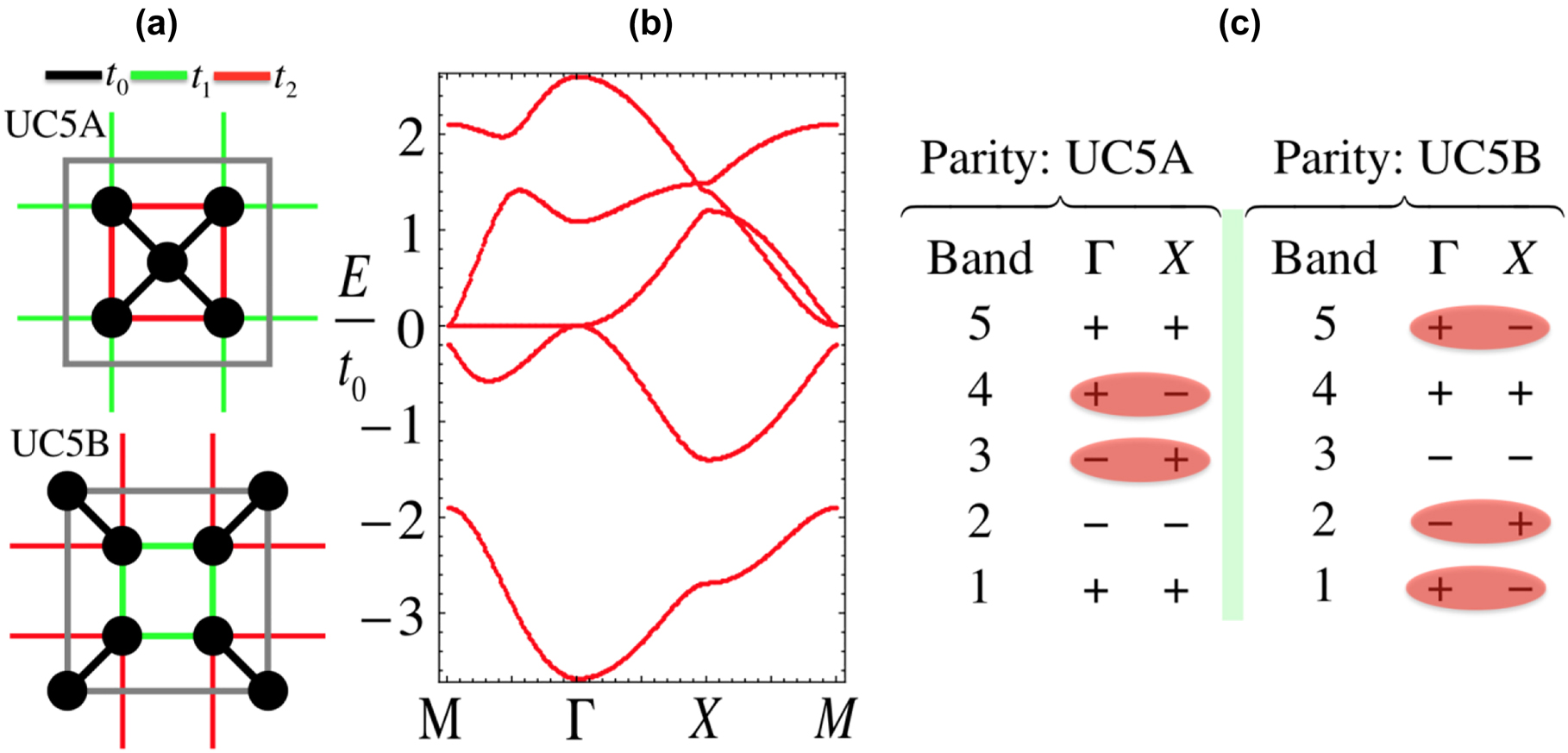
Tight-binding model and results of UC5.
(a) The two unit cells UC5A and UC5B and corresponding hopping patterns described by
Similar analysis could be performed for the other PCs shown in Figure 1. However, as the number of dielectric pillars within the unit cells increases, the tight-binding formualtions would become increasingly complex, where the full-wave simualtions would be more realistic and straightforward. We would like to note that as the tight-binding lattice models are able to capture the key topological features of the optimized PCs in a general way, the topological physics of the PCs with odd-order band gaps discussed in this paper could carry over to diverse system platforms beyond photonics, such as, plasmonics, acoustics, as long as these systems can execute a faithful implementation of the tight-binding model.
Appendix D: Eigenfield distributions of edge states
Figure A2 presents eigenfield distributions of edge states (k || = 0) in Figure 4. The eigenfield distributions from bottom to top for the multiple edge modes correspond to multiple edge states from bottom to top in Figure 4, respectively.
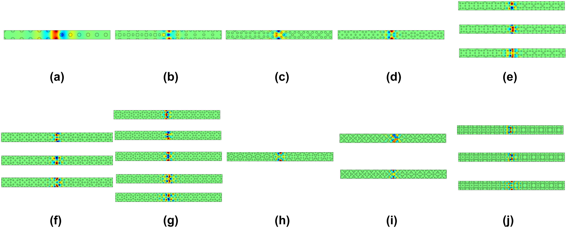
Eigenfield distributions of edge states (k || = 0) for the supercells consisting of (a) UC1A and UC1B, (b) UC3A and UC3B, (c) UC5A and UC5B, (d) UC7A and UC7B, (e) UC9A and UC9B, (f) UC11A and UC11B, (g) UC13A and UC13B, (h) UC15A and UC15B, (i) UC17A and UC17B, and (j) UC19A and UC19B.
References
[1] A. B. Khanikaev and G. Shvets, “Two-dimensional topological photonics,” Nat. Photonics, vol. 11, p. 763, 2017, https://doi.org/10.1038/s41566-017-0048-5.Search in Google Scholar
[2] D. Leykam and L. Yuan, “Topological phases in ring resonators: recent progress and future prospects,” Nanophotonics, vol. 9, pp. 4473–4487, 2020, https://doi.org/10.1515/nanoph-2020-0415.Search in Google Scholar
[3] M. Segev and M. A. Bandres, “Topological photonics: where do we go from here?” Nanophotonics, vol. 10, pp. 425–434, 2021.10.1515/9783110710687-032Search in Google Scholar
[4] M. Kim, W. Gao, D. Lee et al.., “Extremely broadband topological surface states in a photonic topological metamaterial,” Adv. Opt. Mater., vol. 7, p. 1900900, 2019, https://doi.org/10.1002/adom.201900900.Search in Google Scholar
[5] M. Kim, D. Lee, D. Lee, and J. Rho, “Topologically nontrivial photonic nodal surface in a photonic metamaterial,” Phys. Rev. B, vol. 99, p. 235423, 2019, https://doi.org/10.1103/physrevb.99.235423.Search in Google Scholar
[6] F. Haldane and S. Raghu, “Possible realization of directional optical waveguides in photonic crystals with broken time-reversal symmetry,” Phys. Rev. Lett., vol. 100, p. 013904, 2008, https://doi.org/10.1103/PhysRevLett.100.013904.Search in Google Scholar PubMed
[7] S. Raghu and F. D. M. Haldane, “Analogs of quantum-Hall-effect edge states in photonic crystals,” Phys. Rev., vol. 78, p. 033834, 2006.10.1103/PhysRevA.78.033834Search in Google Scholar
[8] L.-H. Wu and X. Hu, “Scheme for achieving a topological photonic crystal by using dielectric material,” Phys. Rev. Lett., vol. 114, p. 223901, 2015, https://doi.org/10.1103/physrevlett.114.223901.Search in Google Scholar PubMed
[9] D. Smirnova, S. Kruk, D. Leykam, E. Melik-Gaykazyan, D.-Y. Choi, and Y. Kivshar, “Third-Harmonic generation in photonic topological metasurfaces,” Phys. Rev. Lett., vol. 123, p. 103901, 2019, https://doi.org/10.1103/physrevlett.123.103901.Search in Google Scholar
[10] Y. Chen, F. Meng, B. Jia, G. Li, and X. Huang, “Inverse design of photonic topological insulators with extra-wide bandgaps,” Phys. Status Solidi Rapid Res. Lett., vol. 13, p. 1900175, 2019, https://doi.org/10.1002/pssr.201900175.Search in Google Scholar
[11] X.-T. He, E.-T. Liang, J.-J. Yuan et al.., “A silicon-on-insulator slab for topological valley transport,” Nat. Commun., vol. 10, p. 872, 2019, https://doi.org/10.1038/s41467-019-08881-z.Search in Google Scholar PubMed PubMed Central
[12] X.-D. Chen, F.-L. Zhao, M. Chen, and J.-W. Dong, “Valley-contrasting physics in all-dielectric photonic crystals: orbital angular momentum and topological propagation,” Phys. Rev. B, vol. 96, p. 020202, 2017, https://doi.org/10.1103/physrevb.96.020202.Search in Google Scholar
[13] X. Ni, D. Purtseladze, D. A. Smirnova, A. Slobozhanyuk, A. Alù, and A. B. Khanikaev, “Spin-and valley-polarized one-way Klein tunneling in photonic topological insulators,” Sci. Adv., vol. 4, pp. 1–9, 2018. https://doi.org/10.1126/sciadv.aap8802.Search in Google Scholar PubMed PubMed Central
[14] M. Saba, S. Wong, M. Elman, S. S. Oh, and O. Hess, “Nature of topological protection in photonic spin and valley Hall insulators,” Phys. Rev. B, vol. 101, p. 054307, 2020, https://doi.org/10.1103/physrevb.101.054307.Search in Google Scholar
[15] Y. Zeng, U. Chattopadhyay, B. Zhu et al.., “Electrically pumped topological laser with valley edge modes,” Nature, vol. 578, pp. 246–250, 2020, https://doi.org/10.1038/s41586-020-1981-x.Search in Google Scholar PubMed
[16] Z. Lan, J. W. You, Q. Ren, W. E. I. Sha, and N. C. Panoiu, “Second-harmonic generation via double topological valley-Hall kink modes in all-dielectric photonic crystals,” Phys. Rev., vol. 103, p. L041502, 2021, https://doi.org/10.1103/physreva.103.l041502.Search in Google Scholar
[17] Z. Zhang, F. Li, J. Lu et al.., “Broadband photonic topological insulator based on triangular-holes array with higher energy filling efficiency,” Nanophotonics, vol. 9, p. 2839, 2020, https://doi.org/10.1515/nanoph-2020-0086.Search in Google Scholar
[18] B. Orazbayev and R. Fleury, “Quantitative robustness analysis of topological edge modes in C6 and valley-Hall metamaterial waveguides,” Nanophotonics, vol. 8, pp. 1433–1441, 2019, https://doi.org/10.1515/nanoph-2019-0137.Search in Google Scholar
[19] Z. Zhang, J. Lu, T. Liu et al.., “Azimuthally and radially polarized orbital angular momentum modes in valley topological photonic crystal fiber,” Nanophotonics, vol. 10, pp. 4067–4074, 2021, https://doi.org/10.1515/nanoph-2021-0395.Search in Google Scholar
[20] W. A. Benalcazar, B. A. Bernevig, and T. L. Hughes, “Quantized electric multipole insulators,” Science, vol. 357, pp. 61–66, 2017, https://doi.org/10.1126/science.aah6442.Search in Google Scholar PubMed
[21] M. Kim, Z. Jacob, and J. Rho, “Recent advances in 2D, 3D and higher-order topological photonics,” Light Sci. Appl., vol. 9, p. 130, 2020, https://doi.org/10.1038/s41377-020-0331-y.Search in Google Scholar PubMed PubMed Central
[22] M. Kim and J. Rho, “Topological edge and corner states in a two-dimensional photonic Su-Schrieffer–Heeger lattice,” Nanophotonics, vol. 9, pp. 3227–3234, 2020, https://doi.org/10.1515/nanoph-2019-0451.Search in Google Scholar
[23] Y. Ota, F. Liu, R. Katsumi et al.., “Photonic crystal nanocavity based on a topological corner state,” Optica, vol. 6, pp. 786–789, 2019, https://doi.org/10.1364/optica.6.000786.Search in Google Scholar
[24] X.-T. He, M.-Y. Li, H.-Y. Qiu et al.., “In-plane excitation of a topological nanophotonic corner state at telecom wavelengths in a cross-coupled cavity,” Photon. Res., vol. 9, pp. 1423–1431, 2021, https://doi.org/10.1364/prj.419569.Search in Google Scholar
[25] W. Zhang, X. Xie, H. Hao et al.., “Low-threshold topological nanolasers based on the second-order corner state,” Light Sci. Appl., vol. 9, p. 109, 2020, https://doi.org/10.1038/s41377-020-00352-1.Search in Google Scholar PubMed PubMed Central
[26] S. S. Kruk, W. Gao, D.-Y. Choi, T. Zentgraf, S. Zhang, and Y. Kivshar, “Nonlinear imaging of nanoscale topological corner states,” Nano Lett., vol. 21, pp. 4592–4597, 2021, https://doi.org/10.1021/acs.nanolett.1c00449.Search in Google Scholar PubMed
[27] Y. Chen, Z. Lan, J. Li, and J. Zhu, “Topologically protected second harmonic generation via doubly resonant high-order photonic modes,” Phys. Rev. B, vol. 104, p. 155421, 2021, https://doi.org/10.1103/physrevb.104.155421.Search in Google Scholar
[28] B. Xie, H.-X. Wang, X. Zhang, et al.., “Higher-order band topology,” Nat. Rev. Phys., vol. 3, pp. 520–532, 2021.10.1038/s42254-021-00323-4Search in Google Scholar
[29] M. Li, D. Zhirihin, M. Gorlach et al.., “Higher-order topological states in photonic kagome crystals with long-range interactions,” Nat. Photonics, vol. 14, pp. 89–94, 2020, https://doi.org/10.1038/s41566-019-0561-9.Search in Google Scholar
[30] B. Xie, G. Su, H.-F. Wang et al.., “Higher-order quantum spin Hall effect in a photonic crystal,” Nat. Commun., vol. 11, p. 3768, 2020, https://doi.org/10.1038/s41467-020-17593-8.Search in Google Scholar PubMed PubMed Central
[31] Y. Chen, F. Meng, Y. Kivshar, B. Jia, and X. Huang, “Inverse design of higher-order photonic topological insulators,” Phys. Rev. Res., vol. 2, p. 023115, 2020, https://doi.org/10.1103/physrevresearch.2.023115.Search in Google Scholar
[32] H.-X. Wang, L. Liang, B. Jiang, J. Hu, X. Lu, and J.-H. Jiang, “Higher-order topological phases in tunable C3 symmetric photonic crystals,” Photon. Res., vol. 9, pp. 1854–1864, 2021, https://doi.org/10.1364/prj.433188.Search in Google Scholar
[33] J. Luo, Z. Du, Y. Guo, C. Liu, W. Zhang, and X. Guo, “Multi-class, multi-functional design of photonic topological insulators by rational symmetry-indicators engineering,” Nanophotonics, vol. 10, pp. 4523–4531, 2021, https://doi.org/10.1515/nanoph-2021-0433.Search in Google Scholar
[34] X.-D. Chen, W.-M. Deng, F.-L. Shi, F.-L. Zhao, M. Chen, and J.-W. Dong, “Direct observation of corner states in second-order topological photonic crystal slabs,” Phys. Rev. Lett., vol. 122, p. 233902, 2019, https://doi.org/10.1103/physrevlett.122.233902.Search in Google Scholar PubMed
[35] B.-Y. Xie, H.-F. Wang, H.-X. Wang et al.., “Second-order photonic topological insulator with corner states,” Phys. Rev. B, vol. 98, p. 205147, 2018, https://doi.org/10.1103/physrevb.98.205147.Search in Google Scholar
[36] B.-Y. Xie, G.-X. Su, H.-F. Wang et al.., “Visualization of higher-order topological insulating phases in two-dimensional dielectric photonic crystals,” Phys. Rev. Lett., vol. 122, p. 233903, 2019, https://doi.org/10.1103/physrevlett.122.233903.Search in Google Scholar PubMed
[37] L. Zhang, Y. Yang, Z.-K. Lin et al.., “Higher-order topological states in surface-wave photonic crystals,” Adv. Sci., vol. 7, p. 1902724, 2020, https://doi.org/10.1002/advs.201902724.Search in Google Scholar PubMed PubMed Central
[38] X. Zhou, Z.-K. Lin, W. Lu, Y. Lai, B. Hou, and J.-H. Jiang, “Twisted quadrupole topological photonic crystals,” Laser Photon. Rev., vol. 14, p. 2000010, 2020, https://doi.org/10.1002/lpor.202000010.Search in Google Scholar
[39] Y. Chen, F. Meng, Z. Lan, B. Jia, and X. Huang, “Dual-polarization second-order photonic topological insulators,” Phys. Rev. Appl., vol. 15, p. 034053, 2021, https://doi.org/10.1103/physrevapplied.15.034053.Search in Google Scholar
[40] F. Liu and K. Wakabayashi, “Novel topological phase with a zero berry curvature,” Phys. Rev. Lett., vol. 118, p. 076803, 2017, https://doi.org/10.1103/PhysRevLett.118.076803.Search in Google Scholar PubMed
[41] G. Yoon, T. Tanaka, T. Zentgraf, and J. Rho, “Recent progress on metasurfaces: applications and fabrication,” J. Phys. Appl. Phys., vol. 54, p. 383002, 2021, https://doi.org/10.1088/1361-6463/ac0faa.Search in Google Scholar
[42] F. Liu, H.-Y. Deng, and K. Wakabayashi, “Helical topological edge states in a quadrupole phase,” Phys. Rev. Lett., vol. 122, p. 086804, 2019, https://doi.org/10.1103/PhysRevLett.122.086804.Search in Google Scholar PubMed
[43] Z. Zhang, H. Long, C. Liu et al.., “Deep‐subwavelength Holey acoustic second‐order topological insulators,” Adv. Mater., vol. 31, p. 1904682, 2019, https://doi.org/10.1002/adma.201904682.Search in Google Scholar PubMed
[44] Z. Zhang, M. R. López, Y. Cheng, X. Liu, and J. Christensen, “Non-Hermitian sonic second-order topological insulator,” Phys. Rev. Lett., vol. 122, p. 195501, 2019, https://doi.org/10.1103/physrevlett.122.195501.Search in Google Scholar
[45] Y. Chen, X. Lu, and H. Chen, “Effect of truncation on photonic corner states in a kagome lattice,” Opt. Lett., vol. 44, pp. 4251–4254, 2019, https://doi.org/10.1364/ol.44.004251.Search in Google Scholar
[46] R. Gong, M. Zhang, H. Li, and Z. Lan, “Topological photonic crystal fibers based on second-order corner modes,” Opt. Lett., vol. 46, pp. 3849–3852, 2021, https://doi.org/10.1364/ol.430579.Search in Google Scholar
[47] M. Proctor, P. A. Huidobro, B. Bradlyn et al.., “Robustness of topological corner modes in photonic crystals,” Phys. Rev. Res., vol. 2, p. 042038, 2020, https://doi.org/10.1103/physrevresearch.2.042038.Search in Google Scholar
[48] J. Zhou, J. Zheng, Z. Fang, P. Xu, and A. Majumdar, “Ultra-low mode volume on-substrate silicon nanobeam cavity,” Opt. Express, vol. 27, pp. 30692–30699, 2019, https://doi.org/10.1364/oe.27.030692.Search in Google Scholar PubMed PubMed Central
[49] F. Meng, X. Huang, and B. Jia, “Bi-directional evolutionary optimization for photonic band gap structures,” J. Comput. Phys., vol. 302, pp. 393–404, 2015, https://doi.org/10.1016/j.jcp.2015.09.010.Search in Google Scholar
[50] J. Nocedal and S. J. Wright, Numerical Optimization, New York, Springer, 1999.10.1007/b98874Search in Google Scholar
[51] K. Svanberg, A Class of Globally Convergent Optimization Methods Based on Conservative Convex Separable Approximations, Philadelphia, Society for Industrial and Applied Mathematics, 2002, pp. 555–573.10.1137/S1052623499362822Search in Google Scholar
© 2022 Yafeng Chen et al., published by De Gruyter, Berlin/Boston
This work is licensed under the Creative Commons Attribution 4.0 International License.
Articles in the same Issue
- Frontmatter
- Reviews
- Gaptronics: multilevel photonics applications spanning zero-nanometer limits
- Ultrafast photonics applications of emerging 2D-Xenes beyond graphene
- Research Articles
- Nonlocal effects in temporal metamaterials
- Pattern-tunable synthetic gauge fields in topological photonic graphene
- Generalized temporal transfer matrix method: a systematic approach to solving electromagnetic wave scattering in temporally stratified structures
- Femtosecond imaging of spatial deformation of surface plasmon polariton wave packet during resonant interaction with nanocavity
- Probing the long-lived photo-generated charge carriers in transition metal dichalcogenides by time-resolved microwave photoconductivity
- Second-order topological phases in C 4v -symmetric photonic crystals beyond the two-dimensional Su-Schrieffer–Heeger model
- Full-visible-spectrum perovskite quantum dots by anion exchange resin assisted synthesis
- Multidimensional engineered metasurface for ultrafast terahertz switching at frequency-agile channels
- High efficiency and large optical anisotropy in the high-order nonlinear processes of 2D perovskite nanosheets
- Dynamic millimeter-wave OAM beam generation through programmable metasurface
- Intelligent metasurface with frequency recognition for adaptive manipulation of electromagnetic wave
- Singularities splitting phenomenon for the superposition of hybrid orders structured lights and the corresponding interference discrimination method
- Inverse-designed waveguide-based biosensor for high-sensitivity, single-frequency detection of biomolecules