Trap-Induced Dispersive Transport and Dielectric Loss in PbS Nanoparticle Films
-
Alina Chanaewa
 ,
Katharina Poulsen
,
Katharina Poulsen

Abstract
In this work, we investigate the electrical and dielectric response of lead sulfide (PbS) nanoparticle (NP) films with impedance spectroscopy. In particular, the influence of the ligand passivation on the surface trap state density of PbS NPs is demonstrated by comparing two different types of ligands: ethane-1,2-dithiol (EDT) and 3-sulfanylpropanoic acid (MPA). We observe that the MPA treatment passivates the PbS surface more efficiently than EDT. By analyzing the dielectric loss spectra, we are able to visualize shallow trap states in the bulk of PbS-EDT films and correlate this with the dispersive response observed in the impedance spectra. Evidence of deep trap states is revealed for both PbS-EDT and PbS-MPA diodes. Under illumination, the PbS-MPA and PbS-EDT films demonstrate almost identical trap profiles, showing solely the deep trap state densities. We conclude that the deep traps are related to the stoichiometry of the PbS NPs.
1 Introduction
In the last decade lead sulfide (PbS) nanocrystals have been extensively investigated in next generation optoelectronic devices. In particular, PbS based solar cells rapidly evolved from <1% devices demonstrated in 2005 [1] to record efficiencies of 11.3% (certified by NREL) by Sargent and coworkers in 2016 [2]. Besides energy conversion, PbS photodetectors [3], [4], [5], [6] and light emitting diodes [7], [8], [9] have been studied. In addition to flexibility offered by solution processing, the major advantage of nanoparticles (NPs) in optoelectronics is the quantum confinement effect, which determines optical and electrical properties by size and shape [10], [11], [12], [13], [14] and can be exploited to tune the light harvesting properties and therefore optimize the absorption in QD solar cells [15], [16].
Generally, performance of NP based optoelectronics is limited either by the loss mechanisms at the device contact interfaces or in the bulk of the NP film. To improve the performance of emerging technologies, it is important to identify where these losses occur. Recent studies on PbS NP films have revealed a complex correlation between trap states and carrier transport. Jeong et al. [17] applied dedicated ligand optimization to increase photocurrent in PbS NP based solar cells, suggesting that surface trap states limit the electrical transport in PbS NP films. A recent study by Bozyigit et al. [18], identified trap states as the major limitation in dark electrical conduction in PbS NP films, and the results indicate that the traps may be related to variations in PbS NP stoichiometry. The observed discrepancy between dark conductivity and photoconductivity in PbS NP films was addressed in a theoretical study by Shabaev et al. who argued that the physical mechanisms of electrical transport are fundamentally different in the dark and under illumination [19]. New experimental approaches are needed to acquire a more complete picture of carrier transport and electrical loss mechanisms in PbS NP films.
In this study, we applied impedance spectroscopy (IS) to investigate the influence of the trap states on electrical transport in PbS NP films. IS can be performed at different bias voltages and under different illumination intensities, so that trap state profiles can be studied under relevant operating conditions on the same working device. Inconsistencies related to variations in measurement conditions for different characterization techniques are therefore avoided.
While IS yields detailed information on the frequency dependent electrical and dielectric response, interpretation of the data is non-trivial and the physical meaning can be only derived by careful design of the experiments. To this end, we used a very simple device structure which comprises a PbS NP layer sandwiched between an indium tin oxide (ITO) and an aluminum electrode. ITO was shown to form an Ohmic contact with the valence band of the PbS, while a Schottky barrier is formed at the PbS-Aluminum interface, yielding rectifying behavior [20].
The devices were prepared using PbS NPs coated with oleic acid obtained from a continuous flow reactor. We varied the bulk properties of the PbS films by using NPs capped with two different type of ligands: ethane-1,2-dithiol (EDT) or 3-sulfanylpropanoic acid (MPA).
To isolate the influence of the contacts, a polyaniline:poly(4-styrenesulfonic acid) (PANI:PSS) interlayer was introduced between the ITO and PbS-EDT or PbS-MPA layer in some devices, and the results were compared to the results from devices prepared without the additional PANI:PSS layer. The energy diagrams of the structures are depicted in Figure 1.
![Fig. 1: Band diagrams of (a) PbS-EDT and (b) PbS-MPA devices showing the workfunction of ITO, Al, the HOMO of the PANI:PSS interlayer and HOMO and LUMO levels as well as the Fermi level (EF) of the PbS films. Energy levels for PbS were calculated using the data from Ref. [21] and the optical bandgap obtained using absorption spectroscopy (see SI). Work function of PANI:PSS was provided by the supplier. For ITO and Al typical values were used.](/document/doi/10.1515/zpch-2016-0906/asset/graphic/j_zpch-2016-0906_fig_001.jpg)
Band diagrams of (a) PbS-EDT and (b) PbS-MPA devices showing the workfunction of ITO, Al, the HOMO of the PANI:PSS interlayer and HOMO and LUMO levels as well as the Fermi level (EF) of the PbS films. Energy levels for PbS were calculated using the data from Ref. [21] and the optical bandgap obtained using absorption spectroscopy (see SI). Work function of PANI:PSS was provided by the supplier. For ITO and Al typical values were used.
Impedance data is commonly displayed in the complex plane, i.e. the Nyquist representation, where the imaginary component of the impedance is plotted against the real component. In the case of electrical or ionic relaxation, the Nyquist plot resembles a semicircle. A single semicircle corresponds to a single relaxation process. Depressed or distorted semicircles indicate multiple relaxation processes or dispersive transport [22]. Frequency dependent information is obtained from Bode plots in which electrical or dielectric parameters are plotted against frequency.
Impedance spectra yield information about the electrical response of the system due to modulations in the electric field. The dielectric response, on the other hand, reflects the ability of a material to store and dissipate energy. The permittivity is also a complex parameter which can be represented in terms of the real component, the dielectric permittivity ε′ and the imaginary component, the dielectric loss ε″,
The dielectric loss spectrum provides information about dissipative energy loss related to dipole reorientation, space charge build up, electronic and ionic relaxation and trapped charge [23].
Polaron relaxation in metal oxide semiconductors has been studied in the literature by investigating temperature and electric field dependent features in the loss dielectric spectra [21], [24], [25].
In this study, we investigate trap-induced dispersive transport in PbS NP films by monitoring dispersive phenomena in the impedance data and correlating this with features in the dielectric loss spectra. Our analysis enables us to distinguish between contact and bulk limited transport, and identify the influence of trapping on the optoelectronic properties of PbS NP films.
2 Experimental section
2.1 Materials
Lead(II)acetate-trihydrate [Pb(OAc)2·3 H2O, 99.99%], diphenylether (≥99%), oleic acid (OA, C18H36O2, ≥90%), acetic acid (C2H4O2≥99.7%), toluene, and dichlorbenzene were purchased from Aldrich. Tri-n-octylphosphine (TOP, C24H51P≥97%) and bis(trimethylsily)sulfide [TMSS, (CH3)3SiSSi(CH3)3, 99%] were purchased from STREM chemicals. Ethan-1,2 dithiol (EDT) was purchased from FLUKA. Acetonitrile was purchased from Chemsolute. PANI:PSS was received from Ormecon GmbH.
2.2 Nanoparticle synthesis
PbS NPs were synthesized in a continuous flow reactor developed by the Centre for Applied Nanotechnology GmbH. A mixture of one equivalent Pb(OAc)2·3 H2O, OA and TOP in diphenylether was heated to 80°C. Acetic acid was evaporated under vacuum to form an OA-lead complex. A 0.5 M solution of bis(trimethylsily)sulfide-TOP was added under nitrogen protection to obtain particles. PbS NPs were isolated from the reaction mixture by precipitation with a polar solvent and subsequent redispersion in octane. The NPs show the absorption edge at 1033 nm, with corresponding band-edge emission at 1166 nm. The mean size of the PbS NPs is approximately 3 nm. High resolution transmission electron microscopy image of the PbS NPs along with optical spectra are presented in Supporting Information.
2.3 Device fabrication
Indium tin oxide (ITO) on a glass substrate was used as a high work function bottom contact. A diode with an area of 16 mm2 was defined by structuring ITO. PANI:PSS was diluted 1:1 with water and spin-coated onto the ITO at 4000 rpm for 1 min and subsequently annealed at 140°C for 1 min. The active layer of PbS NPs was spincoated using an in situ ligand exchange approach. First, a highly concentrated PbS NP solution was spincoated at 1500 rpm followed by a mixture of acetonitrile and EDT (0.1 M). Next, actetonitrile and octane were used to remove the ligand excess. This procedure was repeated up to four times to replace the original ligand and to manufacture a PbS layer of approx. 180 nm thickness. Aluminum was evaporated on the active layer through a shadow mask to form the low work function top contact.
2.4 Electrical measurements
The impedance measurements were performed using Nova Autolab PGSTAT302N potentiostat equipped with the FRA32M frequency analyzer module. The applied AC voltage was set to 20 mV and the DC voltage offset was chosen between −0.5 V and 0.5 V. The frequency was swept from 1 MHz and 10 Hz. To avoid disturbance from any background noise, the sample was placed into a Faraday cage for the duration of the measurement. Measurements under illumination were recorded using LOT LS 0306 Solar Simulator equipped with 1.5 AM filter and 100 mW/cm2 irradiation power.
3 Results
3.1 Impedance and dielectric properties of PbS NP films in the dark
Figure 3 shows the Nyquist plot of the impedance recorded for the samples. The data taken from PbS films capped with the EDT ligand are shown as black squares (with PANI:PSS interlayer) and green triangles (without PANI:PSS interlayer), respectively. The data taken from PbS films capped with MPA ligands are shown as red circles (with PANI:PSS interlayer) and blue triangles (without PANI:PSS interlayer), respectively. We observe that the samples demonstrate a high capacitive component, i.e. the semicircles do not close at lower frequencies. To understand the influence of the PANI:PSS interlayer and ligands in more detail, we fit the impedance data using the circuit model consisting of one R-CPE and one RC element (Figure 2). The constant phase element (CPE1) accounts for non-idealities in the system response, i.e. dispersive transport. The impedance of the CPE is given by
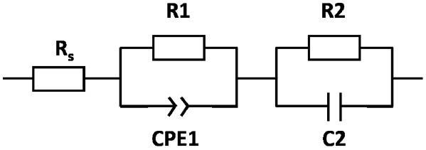
Equivalent circuit diagram used for fitting impedance data in this study.
where Q is the effective coefficient, and α is a unit-less parameter between 0 and 1. If α=1, Q reduces to an ideal capacitor Q=C and if α=0, the CPE reduces to an ideal resistor Q=1/R.
Fits are represented as solid lines in Figure 3 and the details of the fitting analysis can be found in the Supporting Information.

Nyquist plot for the devices used in this study including fits at 0 V bias. For convenience PANI is used instead of PANI:PSS in the legend.
We now consider the voltage-dependence of the circuit elements. The series resistance Rs was found to be voltage independent and very comparable between the samples, with values in the range of 125–155 Ohm cm−2, whereas resistances R1 and R2 exhibit bias dependent change, which we attribute to field-induced variations in Schottky barrier height. Ligands at the NP surface act as interface dipoles leading to changes in doping density and therefore alter the Fermi level of PbS [26], [27]. Depending on the electronic character of the ligands, NPs can exhibit either p- or n-type, as well as ambipolar transport. The energetic position of the Fermi level in NP films treated with EDT is expected to be close to the middle of the band gap, whereas MPA treated samples were shown to be rather p-doped with the Fermi level closer to the valence band. The variation in the position of the Fermi level for differently treated samples leads to variation in Schottky barrier height at the PbS-Al interface [20], which is qualitatively larger in the case of MPA treated samples and therefore shows higher values in R1 and R2 (see Supporting Information).
The most intriguing behavior is observed in the CPE element values. α values are shown in Figure 6, they were found to be between 0.95 and 0.99 for devices prepared with MPA ligand and 0.85–0.97 for devices prepared with EDT (Figure 4a). The effective CPE coefficient Q increases for EDT devices by one order of magnitude for negative bias, indicative of charge build up, whereas the values for MPA devices show little dependence on bias voltage (Figure 4b). A decrease in α and increase in Q for EDT treated samples strongly indicate the presence of trap states, which manifest themselves as a distribution in carrier mobilities due to multiple trapping and release processes (α) and space charge (Q) [28], [29]. Experimentally, it was shown that EDT ligands introduce a higher density of trap states in the band gap of the PbS NPs compared to MPA [17]. Theoretical studies support these findings [30] demonstrating the emergence of gap states in PbS density of states structure for increased concentrations of EDT and for various binding configurations, i.e. mono- or bidentate. In the dark, the impedance spectra demonstrate that dispersive transport in EDT devices is prevalent, indicating that the electrical transport is bulk-limited. In contrast, the use of MPA ligands leads to better surface passivation, and therefore decreases trap state density. In these devices, the electrical transport seems to be rather limited by the Schottky interface, as inferred from voltage-dependent variations in the circuit element R2.
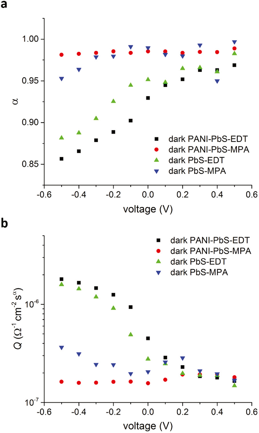
(a) α values and (b) Q values plotted against bias voltage for PbS-EDT devices with PANI:PSS interlayer (black squares) and without (green triangles), as well as for PbS-MPA with (red dots) and without PANI:PSS interlayer (blue triangles). α and Q were obtained from fits using the circuit model displayed in Figure 2.
The voltage-dependent dielectric loss spectra of NP films prepared with EDT and MPA ligands are shown in Figure 5a and b, respectively. We observe two peaks in the loss spectra of NPs films prepared with EDT (Figure 5a). The low frequency peak clearly demonstrates bias dependence, while the high frequency peak is bias independent. For MPA treated NP films, the low frequency peak is absent.
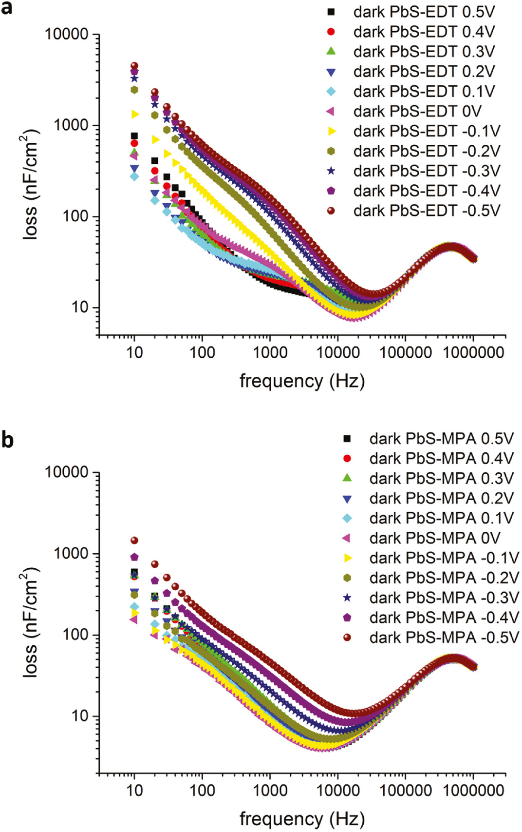
Representation of loss versus frequency for (a) PbS-EDT and (b) PbS-MPA diodes without the PANI:PSS interlayer for bias voltages in the range between +0.5 V and −0.5 V.
From the equivalent circuit analysis, we attribute the peak in the lower frequency range to the shallow traps in PbS induced by EDT, that yield the dispersive transport and is reflected in CPE parameters α and Q. We assign the frequency independent peak at high frequency to the deep traps in PbS quantum dots [30], [31], which were observed next to the shallow traps [17], [31].
To visualize shallow and deep trap states, we applied the model from Walter et al. [32]. In this model, variations in semiconductor capacitance with frequency are proportional to the energetic distribution of trap states NT according to
From the plot of the derivative of dC/dω versus frequency (Figure 6) we observe features which can be attributed to the presence of shallow trap state densities (low frequencies) for EDT treated NP films, and the presence of deep trap state densities (high frequencies) which peak at around the same frequency for all devices. This might point to the traps originated from the stoichiometry of the PbS nanocrystals (ratio of Pb:S) [30].
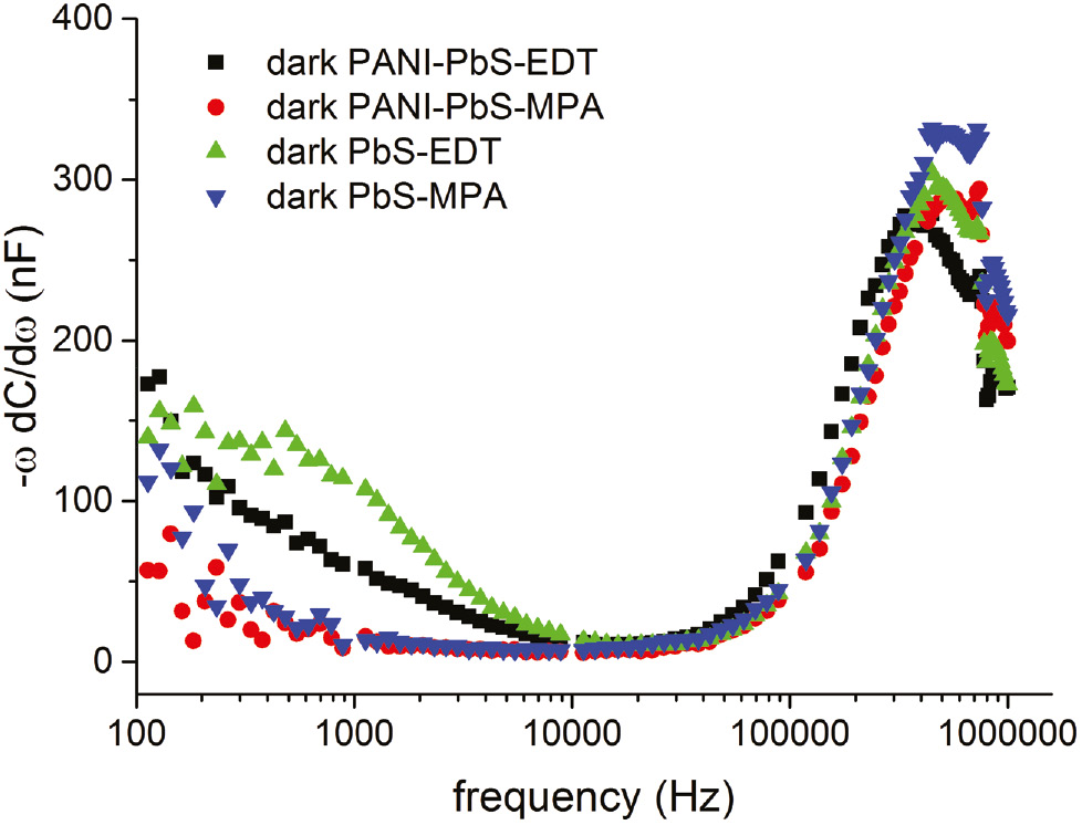
Plot of the frequency dependent derivative of the capacitance for PbS-EDT diodes with (black squares) and without PANI:PSS interlayer (green triangles) as well as PbS-MPA diodes with (red circles) and without PANI:PSS interlayer (blue triangles) at 0 V bias. −ωdC/dω is proportional to the density of trap states and represent a trap states profile once plotted against frequency.
3.2 Impedance and dielectric properties of PbS NP films under illumination
Interestingly, under illumination the values of the circuit elements are very comparable for all devices (see Supporting Information). The CPE element reduces to a nearly ideal capacitor with frequency independent values, with α in the range of 0.96–0.98. We only notice variations in R1 with voltages in forward bias conditions and it was earlier attributed to the change in Schottky barrier. All of the other circuit element values are bias voltage independent. Generally, we observe an overall increase in capacitances and decrease in resistances for all devices. This is consistent with an increase in photo-generated charge density in the active layer, which facilitates trap filling [33].
Under illumination, the peak in the dielectric loss spectrum associated with shallow traps is no longer observed and deep trap peak is shifted to lower frequencies (Figure 7a). This behavior can be understood by considering the dC/dω versus frequency spectrum (Figure 7b). Variations in device capacitance are correlated to the trapping and release of carriers in states, assumed to be symmetrically centered around EF [32]. Under illumination, photoinduced charge and trap filling results in shifting of EF in the band gap. The analysis is not sensitive to the energetic direction of shifts in EF, only differences in energy. Figure 7a and b together indicate that under illumination, the energy difference between EF and the density of deep trap states diminishes.
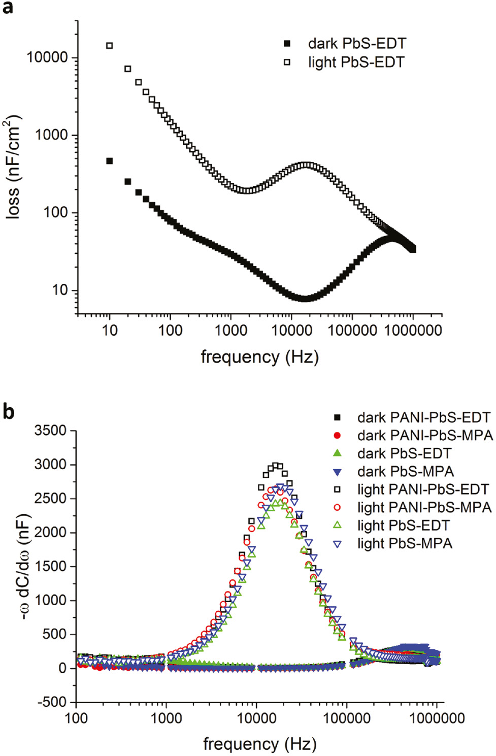
(a) Loss spectra of PbS-EDT diode in dark (filled squares) and under illumination (open squares) at 0 V bias and (b) −ωdC/dω plotted against frequency for PbS-EDT and PbS-MPA diodes in dark (filled symbols) and under illumination (open symbols) displaying the trap states profiles of the devices in dark and under illumination. The dark trap states profile is the same as displayed in Figure 6.
Our impedance results demonstrate that PbS NP films prepared with the two different ligands demonstrate different trap profiles in the dark, but the same trap profiles under illumination. The results from the dark measurements are consistent with the findings from the study by Jeong et al. [17], in which it is reported that MPA is more effective for passivating surface states than EDT. Under illumination, however, we observe that the influence of the ligand on electrical transport vanishes, and electrical transport is limited by deep trap states related to PbS stoichiometry. The change in the electrical and dielectric properties of the PbS NP films upon illumination may be attributed to photoinduced trap filling of shallow surface states. However, it has also been argued that the increase in carrier density upon illumination cannot explain the relatively high values of photoconductivity observed in PbS NP films [19]. At high carrier densities increased carrier delocalization has been reported [34]. These results indicate that more detailed studies of carrier transport under different illumination conditions are necessary to fully understand electrical loss mechanisms in PbS NP films for opto-electronic applications.
In summary, we find that trap-induced dispersive transport plays a greater role in the dark and at lower devices biases, i.e. for LED applications. Under illumination, however, stoichiometric defects which induce deeper traps in the PbS nanoparticles may be more relevant for device performance.
4 Conclusions
We applied impedance spectroscopy to investigate the influence of trap states on dispersive transport phenomena in PbS NP films. PbS NPs were prepared using a continuous flow reactor. To identify the role of surface defects on electrical transport, we used NP films treated with two different ligands, EDT and MPA. PbS NP diodes were prepared with and without a PANI:PSS interlayer to isolate the influence of the device contacts. In the dark we observe that MPA leads to better surface passivation of the NPs than EDT, resulting in negligible dispersive phenomena in the electrical transport properties. As a result, NP films prepared with MPA show stronger evidence of contact limited transport, while NP films prepared with EDT demonstrate stronger evidence of bulk limited transport. Under illumination, the trap profiles of the devices are observed to be nearly identical. We conclude that under illumination photocharge generation in the NP films facilitates trap filling. As a result, surface traps are observed in the impedance spectra taken in the dark, while under illumination deeper trap states related to the stoichiometry of PbS NPs dominate the dielectric loss spectra. Our results demonstrate the utility of correlating impedance modeling with analysis of the dielectric loss spectrum to quantify trap-induced dispersive transport in NP semiconductors for opto-electronics.
References
1. S. A. McDonald, G. Konstantatos, S. Zhang, P. W. Cyr, E. J. D. Klem, L. Levina, E. H. Sargent, Nat. Mater. 4, 138 (2005).10.1038/nmat1299Search in Google Scholar PubMed
2. A. Kiani, H. F. Movahed, S. Hoogland, O. Voznyy, R. Wolowiec, L. Levina, F. P. G. de Arquer, P. Pietsch, X. Wang, P. Maraghechi, E. H. Sargent, ACS Energy Lett. 1, 740 (2016).10.1021/acsenergylett.6b00314Search in Google Scholar
3. D. Kufer, I. Nikitskiy, T. Lasanta, G. Navickaite, G. Konstantatos, Adv. Mater. 27, 176 (2014).10.1002/adma.201402471Search in Google Scholar PubMed
4. Z. Sun, Z. Liu, J. Li, G.-A. Tai, S.-P. Lau, F. Yan, Adv. Mater. 24, 5878 (2012).10.1002/adma.201202220Search in Google Scholar PubMed
5. V. Sukhovatkin, S. Hinds, L. Brzozowski, E. H. Sargent, Science 324, 1542 (2009).10.1126/science.1173812Search in Google Scholar PubMed
6. G. Konstantatos, I. Howard, A. Fischer, S. Hoogland, J. Clifford, E. Klem, L. Levina, E. H. Sargent, Nature 442, 180 (2006).10.1038/nature04855Search in Google Scholar PubMed
7. L. Sun, D. Stachnik, B.-R. Hyun, T. Hanrath, Nature Nanotechnol. 7, 369 (2012).10.1038/nnano.2012.63Search in Google Scholar PubMed
8. X. Ma, F. Xu, J. Benavides, Org. Electron. 13, 525 (2012).10.1016/j.orgel.2011.12.012Search in Google Scholar
9. Z. Yang, O. Voznyy, M. Liu, M. Yuan, A. H. Ip, O. S. Ahmed, L. Levina, S. Kinge, S. Hoogland, E. H. Sargent, ACS Nano 9, 12327 (2015).10.1021/acsnano.5b05617Search in Google Scholar PubMed
10. M. A. El-Sayed, Acc. Chem. Res. 37, 326 (2004).10.1021/ar020204fSearch in Google Scholar PubMed
11. M. Grätzel, Nature 414, 338 (2001).10.1038/35104607Search in Google Scholar PubMed
12. L. Li, J. Hu, W. Yang, A. P. Alivisatos, Nano Lett. 1, 349 (2001).10.1021/nl015559rSearch in Google Scholar
13. L. Brus, J. Phys. Chem. 90, 2555 (1986).10.1021/j100403a003Search in Google Scholar
14. Z. Hens, D. Vanmaekelbergh, E. J. A. J. Stoffels, H. van Kempen, Phys. Rev. Lett. 88, 236803-1 (2002).10.1103/PhysRevLett.88.236803Search in Google Scholar PubMed
15. S. Rühle, M. Shalom, A. Zaban, ChemPhysChem 11, 2290 (2010).10.1002/cphc.201000069Search in Google Scholar PubMed
16. X. Wang, G. I. Koleilat, J. Tang, H. Liu, I. J. Kramer, Nat. Photonics 5, 480 (2011).10.1038/nphoton.2011.123Search in Google Scholar
17. K. S. Jeong, J. Tang, H. Liu, J. Kim, A. W. Schaefer, K. Kemp, L. Levina, X. Wang, S. Hoogland, R. Debnath, L. Brzozowski, E. H. Sargent, J. B. Asbury, ACS Nano 6, 89 (2012).10.1021/nn2039164Search in Google Scholar PubMed
18. D. Bozyigit, W. M. M. Lin, N. Yazdani, O. Yarema, V. Wood, Nat. Commun. 6, 6180 (2015).10.1038/ncomms7180Search in Google Scholar PubMed PubMed Central
19. A. Shabaev, A. L. Efros, A. L. Efros, Nano Lett. 13, 5454 (2013).10.1021/nl403033fSearch in Google Scholar PubMed
20. J. P. Clifford, K. W. Johnston, L. Levina, E. H. Sargent, Appl. Phys. Lett. 91, 253117 (2007).10.1063/1.2823582Search in Google Scholar
21. W. Z. Yang, C. L. Song, X. Q. Liu, H. Y. Zhu, X. M. Chen, J. Mater. Sci. 46, 6339 (2011).10.1007/s10853-011-5580-ySearch in Google Scholar
22. E. Barsoukov, J. R. Macdonald, Impedance Spectroscopy: Theory, Experiment, and Applications, John Wiley & Sons, Inc., Hoboked, New Jersey, USA, 2nd ed. (2005).10.1002/0471716243Search in Google Scholar
23. A. K. Jonscher, J. Phys D Appl. Phys. 32, R57 (1999).10.1088/0022-3727/32/14/201Search in Google Scholar
24. O. Bidault, M. Maglione, M. Actis, M. Kchikech, B. Salce, Phys. Rev. B 52, 4191 (1995).10.1103/PhysRevB.52.4191Search in Google Scholar
25. W. C. Ribeiro, E. Joanni, R. Savu, P. R. Bueno, Solid State Commun. 151, 173 (2011).10.1016/j.ssc.2010.10.034Search in Google Scholar
26. P. R. Brown, D. Kim, R. R. Lunt, N. Zhao, M. G. Bawendi, J. C. Grossman, V. Bulović, ACS Nano 8, 5863 (2014).10.1021/nn500897cSearch in Google Scholar PubMed
27. O. Voznyy, D. Zhitomirsky, P. Stadler, Z. Ning, ACS Nano 6, 8448 (2012).10.1021/nn303364dSearch in Google Scholar PubMed
28. J. F. Rubinson, Y. P. Kayinamura, Chem. Soc. Rev. 38, 3339 (2009).10.1039/b904083hSearch in Google Scholar PubMed
29. J. Bisquert, Physi. Rev. B 77, (2008).10.1103/PhysRevB.77.235203Search in Google Scholar
30. D. Kim, D.-H. Kim, J.-H. Lee, J. C. Grossman, Phys. Rev.Lett. 110, (2013).10.1103/PhysRevLett.110.196802Search in Google Scholar PubMed
31. A. A. Bakulin, S. Neutzner, H. J. Bakker, L. Ottaviani, D. Barakel, Z. Chen, ACS Nano 7, 8771 (2013).10.1021/nn403190sSearch in Google Scholar PubMed
32. T. Walter, R. Herberholz, C. Müller, H. W. Schock, J. Appl. Phys. 80, 4411 (1996).10.1063/1.363401Search in Google Scholar
33. G. Konstantatos, J. Clifford, L. Levina, E. H. Sargent, Nat. Photonics 1, 531 (2007).10.1038/nphoton.2007.147Search in Google Scholar
34. E. Talgorn, Y. Gao, M. Aerts, L. T. Kunneman, J. M. Schins, T. J. Savenije, M. A. van Huis, H. S. J. van der Zant, A. J. Houtepen, L. D. A. Siebbeles, Nat. Nanotech. 6, 733 (2011).10.1038/nnano.2011.159Search in Google Scholar PubMed
Supplemental Material:
The online version of this article (DOI: 10.1515/zpch-2016-0906) offers supplementary material, available to authorized users.
©2017 Walter de Gruyter GmbH, Berlin/Boston
Articles in the same Issue
- Frontmatter
- Editorial
- Hierarchical Colloidal Nanostructures – from Fundamentals to Applications
- One-Pot Synthesis of Cationic Gold Nanoparticles by Differential Reduction
- Impact of the Crosslinker’s Molecular Structure on the Aggregation of Gold Nanoparticles
- Modeling the Optical Responses of Noble Metal Nanoparticles Subjected to Physicochemical Transformations in Physiological Environments: Aggregation, Dissolution and Oxidation
- Tetrazole-Stabilized Gold Nanoparticles for Catalytic Applications
- Catalytic Properties of Cryogelated Noble Metal Aerogels
- Graded Shells in Semiconductor Nanocrystals
- Determination of all Dimensions of CdSe Seeded CdS Nanorods Solely via their UV/Vis Spectra
- Ultrafast Transient Absorption and Terahertz Spectroscopy as Tools to Probe Photoexcited States and Dynamics in Colloidal 2D Nanostructures
- Trap-Induced Dispersive Transport and Dielectric Loss in PbS Nanoparticle Films
- Towards Photo-Switchable Transport in Quantum Dot Solids