Ultrafast Transient Absorption and Terahertz Spectroscopy as Tools to Probe Photoexcited States and Dynamics in Colloidal 2D Nanostructures
-
 ,
,

Abstract
Two-dimensional (2D) semiconductors hold high potential for the implementation of efficient ultrathin electronics (e.g. field-effect transistors, light emitting diodes and solar cell devices). In recent years, colloidal methods to synthesize ultrathin 2D materials have been developed that offer alternatives (like the production of non-layered 2D materials and upscaling) to mechanical exfoliation methods. By focusing on optoelectronic applications, it is important to characterize the nature and dynamics of photoexcited states in these materials. In this paper, we use ultrafast transient absorption (TA) and terahertz (THz) spectroscopy as optimal tools for such a characterization. We choose recently synthesized ultrathin colloidal 2D InSe nanosheets (inorganic layer thickness 0.8–1.7 nm; ≤5 nm including ligands) for discussing TA and THz spectroscopic studies and elucidate their charge carrier dynamics under photoexcitation with TA. THz spectroscopy is then used to extract contactless AC mobilities as high as 20±2 cm2/Vs in single InSe layers. The obtained results underpin the general applicability of TA and THz spectroscopy for characterizing photoexcited states in 2D semiconductors.
1 Introduction
Ultrathin 2D semiconductor materials with a (tunable) band gap have the potential to revolutionize next generation electronics. They are mainly synthesized by exfoliation techniques or colloidal methods and exhibit highly promising optoelectronic properties different from their bulk or nanocrystal counterparts [1], [2], [3], [4], [5], [6]. We use ultrafast transient absorption (TA) and terahertz (THz, 1 THz=1012 Hz) spectroscopy, to investigate exciton and charge carrier formation, mobility and decay dynamics in 2D semiconductors. An advantage of TA as compared to commonly used (time-resolved) photoluminescence (PL) spectroscopy is its sensitivity to non-emissive and dark states, which cannot be probed by photoluminescence spectroscopy. This significantly enhances the spectroscopic characterization possibilities for weakly or non-emitting states in semiconductors (like 2D InSe nanosheets). THz spectroscopy is used to differentiate between the formation of excitons and free charges in photoexcited semiconductors. For optoelectronic applications usually the formation of free charges is favored for efficient transistors and solar cells, while the formation of luminescing excitons is beneficial for light emitting diodes.
We discuss recent TA and THz measurements on ultrathin 2D InSe nanosheets, a material with highly interesting optoelectronic properties that also underpin the general applicability of both methods for an in-depth spectroscopic characterization of 2D semiconductors [7].
1.1 Optical pump – optical/THz probe spectroscopy
Optical pump – optical/terahertz probe spectroscopy is a summarizing term for spectroscopic methods where an optical pump pulse is used to photoexcite electrons across the band gap of a semiconductor. A second delayed optical or THz probe pulse is used to study the sample response at different times after photoexcitation, allowing to draw conclusions on the nature of the photoexcited states (excitons, free charge carriers) as well as the mechanism of their decay as a function of time [8], [9]. The term pump refers to the portion of the laser beam that is used to photoexcite the sample, while the term probe refers to the portion of the laser beam, which is used to monitor the sample response at different times after photoexcitation. The underlying charge carrier processes in a wavelength or frequency region of the electromagnetic spectrum can thus be interpreted by their time-evolution. In this article we focus on the optical TA and THz conductivity detection with pulsed lasers (pulse duration 60–200 fs), enabling an ultrafast time resolution.
After leaving the laser, the fundamental beam is split, so that a high-energy portion of it constitutes the pump beam. The main portion of the fundamental laser beam of both, the TA (Yb:KGW laser) and THz (Ti:sapphire laser) set-up, is led into an optical parametric amplifier (OPA). Here, the photoexcitation wavelength of choice (between 266–2100 nm in our set-ups) is generated by non-linear processes including second harmonic and difference frequency generation. By chopping every other pump laser pulse in the TA and THz set-up, differential (ground state compared to excited state) absorption and THz spectra are obtained.
The low energy portion of the fundamental laser beam constitutes the probe beam. Focusing of the fundamental wavelength (1028 nm, pulse duration 200 fs) of the Yb:KGW laser probe beam onto a sapphire crystal in the TA set-up leads to the formation of a white light continuum (by non-linear processes) in the wavelength range of interest (in our case 380–1500 nm). Focusing of a small portion of the fundamental wavelength (800 nm, 60 fs) of the Ti:sapphire laser onto a non-linear LiNbO3 crystal leads to the generation of a single-cycle THz frequency probe pulse, which is detected in a non-linear ZnTe crystal. The transient THz electrical field generated in the LiNbO3 and changed by the photoexcited sample response is compared to the original THz electrical field of the sample in the ZnTe crystal by electro-optical sampling [10], [11], [12].
A time-resolved spectrum is generated by varying the pump-probe delay, while consecutively scanning the sample response at different times after the photoexcitation. This allows drawing conclusions about the exciton and/or charge carrier dynamics and recombination processes as a function of time.
In this respect, TA and THz spectroscopy described here are both following the same concept: The photoexcitation of a sample with an optical pump pulse and the investigation of the sample at given times after photoexcitation with
THz spectroscopy can be used for a contact-less determination of the AC conductivity/mobility in semiconductor samples. Unlike FET mobility measurements, it is insensitive to contact resistances and yields the intrinsic mobility of the sample before charge carrier trapping occurs [11].
1.2 Colloidal ultrathin InSe nanosheets
InSe is a van der Waals layered bulk semiconductor with highly promising photodetecting properties and FET mobilities of up to 1000 cm2/Vs [13], [14], [15]. By colloidal methods, atomically thin mono/double layers of InSe can be obtained (inorganic layer thickness 0.8–1.7 nm, ≤5 nm including ligands), a thickness hardly accessible by exfoliation methods [16]. Figure 1a shows a TEM image of multiple stacked InSe layers separated from each other by their stabilizing ligand decylamine. Generally, primary amine ligands in the InSe nanosheet synthesis serve as mesophase ligand-template for the growth and stabilization of ultrathin InSe nanosheets. Using decyl- and octadecylamine as stabilizing ligands we obtain InSe nanosheets with the same thickness [as visible from the same absorption near 600 nm (2.1 eV) in Figure 1b]. The lateral size of the nanosheets increases from 300–800 nm for octadecylamine as a ligand to 1–2 μm when changing the ligand to decylamine [7], [16].
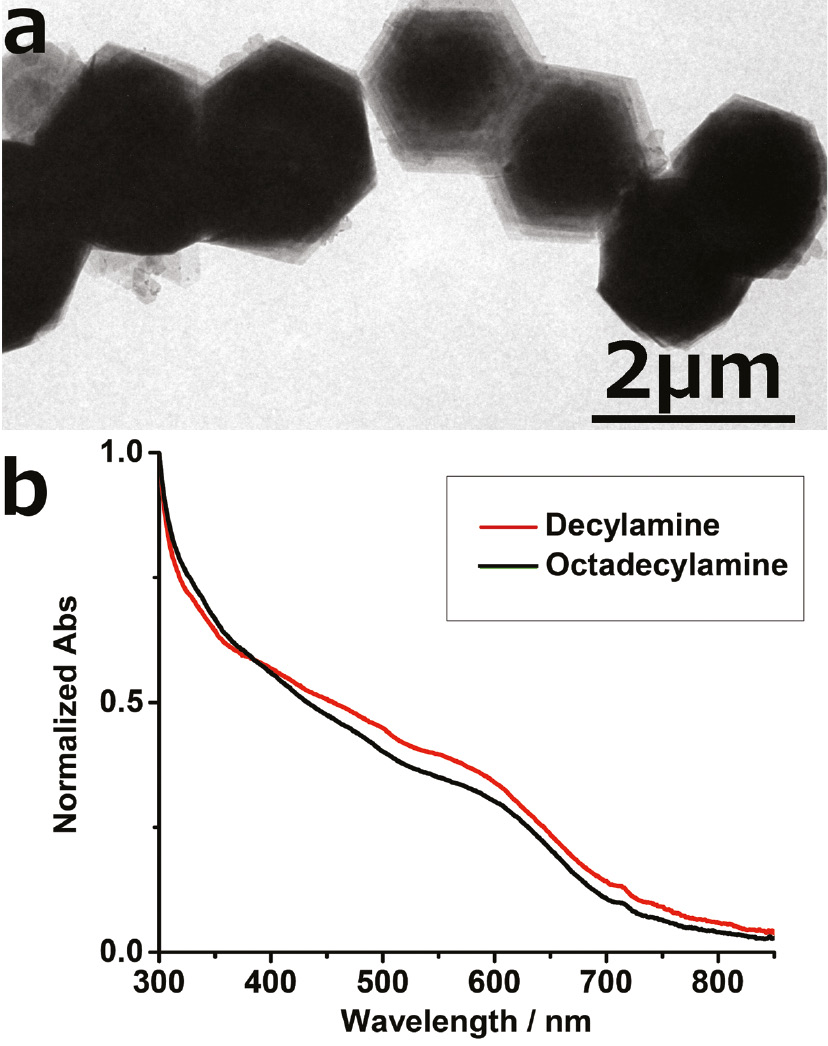
(a) TEM image of ultrathin InSe nanosheets stabilized with decylamine, (b) steady-state absorption spectra of InSe nanosheets, stabilized with decyl- and octadecylamine, respectively, exhibiting the same absorption near 600 nm and hence the same thickness of the inorganic InSe layer of 0.8–1.7 nm.
InSe nanosheets show weak photoluminescence near 600 nm [16], assumedly originating from the slightly indirect band gap of mono/double InSe layers as predicted by DFT calculations [7]. TA and THz spectroscopy are used to characterize the exciton and charge carrier dynamics and mobility in InSe nanosheets.
2 Transient absorption (TA)
TA has been successfully applied for studying a high carrier multiplication (CM) efficiency in 2D PbS nanosheets [17]. CM is a process where the photoexcitation by a single high-energy photon creates multiple electron-hole pairs potentially useful for increasing solar cell efficiencies. An advantage of TA as compared to (time-resolved) PL measurements is that it provides information about the charge carrier (recombination) dynamics of both, radiative and non-radiative processes. This makes TA advantageous for disentangling non-radiative recombination ways like charge trapping or Auger recombination or for characterizing indirect band gap semiconductors.
Figure 2a shows a scheme of the TA set-up. The sample is photoexcited by a 200 fs pump pulse, while the time-delayed probe pulse is used to study the change in its absorption at different times after photoexcitation. The pump pulse is dumped after traversing the sample and the probe pulse is detected. Figure 2b shows the signals, which are detected [18]. Photoexcitation of the sample leads to a ground-state bleach (negative ΔA signal) as part of the electrons is photoexcited from the ground state to excited states. The absorbing share of electrons in the ground state of the photoexcited sample is thus reduced as compared to the ground state absorption of the unexcited sample and a negative ΔA signal is obtained. Stimulated emission of excited electrons back to the ground state can occur when the probe pulse passes the sample (negative ΔA signal). Stimulated emission is only occurring for allowed optical transitions and roughly follows the PL shape of the sample (see Figure 2c). Note that the weak intensity of the probe pulse only leads to a depopulation of a small fraction of the excited states of the sample. Induced absorption of photoexcited electrons to higher excited states or intraband transitions lead to a positive ΔA signal (see Figure 2c). The measured signal is the sum of all these contributions.
![Fig. 2: (a) Scheme of the TA set-up with the pump pulse photoexciting the sample, while the probe pulse is used to monitor the sample response at different times after photoexcitation, (b) contributions to the ΔA spectrum shown in (c) with a negative ΔA signal from the ground-state bleach and stimulated emission and a positive ΔA signal originating from excited-state absorption, (c) bleach (dashed line), stimulated emission (dotted line), excited-state absorption (solid line), sum of these contributions (thick line). Reprinted with permission from ref. [18], Copyright 2009 Springer.](/document/doi/10.1515/zpch-2016-0911/asset/graphic/j_zpch-2016-0911_fig_002.jpg)
(a) Scheme of the TA set-up with the pump pulse photoexciting the sample, while the probe pulse is used to monitor the sample response at different times after photoexcitation, (b) contributions to the ΔA spectrum shown in (c) with a negative ΔA signal from the ground-state bleach and stimulated emission and a positive ΔA signal originating from excited-state absorption, (c) bleach (dashed line), stimulated emission (dotted line), excited-state absorption (solid line), sum of these contributions (thick line). Reprinted with permission from ref. [18], Copyright 2009 Springer.
Figure 3a shows the 2D TA spectrum of decylamine-stabilized InSe nanosheets (photoexcited at 480 nm, 2.6 eV). The ground-state bleach in the TA spectrum with a maximum at 620 nm (2.0 eV) matches the steady-state absorption of InSe nanosheets near 600 nm. The bleach is long-lived and has not decayed completely after 2.5 ns, the measurement-range of the TA set-up (see Figure 3b). The decay shown in Figure 3c becomes faster at higher photoexcitation densities per unit area. This means that higher order recombination processes (radiative ones and non-radiative Auger recombination) become more important at higher photoexcitation densities.

(a) 2D TA spectrum of InSe nanosheets, showing the wavelength spectrum as a function of time-delay between pump and probe pulse with a ground-state absorption bleach at 620 nm (2.0 eV) close to the steady-state absorption near 600 nm (2.1 eV), (b) TA spectra of InSe nanosheets at different times after photoexcitation, showing a long-lived lived bleach (>2.5 ns), (c) faster decay kinetics in InSe nanosheets at higher photoexcitation densities due to higher order recombination processes.
3 Excitons and/or free charges?
While the formation of Coulombically bound excitons under photoexcitation is favorable for electronic applications where high PL efficiencies are needed (e.g. light-emitting diodes), the formation of free charges under photoexcitation is beneficial for solar cell devices. TA is sensitive to the sum of the electron and hole population densities and thus probes the sum of free charge carriers and Coulombically bound excitons, but it lacks the ability to distinguish between these species. For disentangling the contribution of excitons and/or free charges in a photoexcited sample and to determine the sample’s “intrinsic” conductivity/mobility, THz spectroscopy can be used [7].
4 Terahertz (THz) spectroscopy/conductivity
Figure 4 shows a scheme of the THz set-up. The sample is excited with 60 fs pulses, while its response is probed with the THz electrical field [7], [10], [11], [12], [19], [20]. The photoconductivity caused by photoexcited excitons and free charges is determined by measuring the reduction of the amplitude and the phase shift of the THz electrical field by the sample. This yields the conductivity Δσ(ω,t) as a function of the frequency, f=ω/2π, of the probing THz field at a varying time t after the pump pulse. The frequency dependent conductivity due to charges is determined by the field-induced drift velocity in the oscillating THz electric field E(t)=E0cos(ω,t). The complex valued mobility of charges and excitons can be related to three different velocity components in the THz field: (1) The velocity of free charges in-phase with the THz field (see Figure 4) v(t)=μR (ω)E0cos(ω,t) with μR (ω) the real component of the charge mobility, (2) the velocity of free charges out-of-phase with the THz field v(t)=μI (ω)E0sin(ω,t), with μI (ω) the imaginary component of the charge mobility, and (3) the relative out-of-phase velocity of an electron and hole that are Coulombically bound veh (t)=μI (ω)E0sin(ω,t) with

Scheme of the THz spectroscopy set-up with free charges moving in-phase with the electrical field of the THz radiation and reducing its amplitude by absorbing the THz radiation, free charges moving out-of-phase with the THz field and polarizable excitons, causing a phase-lag of the probing THz field.
From the measurements we obtain the differential transmission of the THz waveform ΔE(tp ,t)=Eexcited(tp ,t)–E0(tp ) with Eexcited(tp ,t), the transmitted THz electric field after photoexcitation of the sample and E0(tp ), the transmitted THz electric field in absence of photoexcitation (tp is the time between generating and detecting the THz field and t the time delay between the photoexcitation pump pulse and the THz probe pulse). ΔE(tp ,t) is normalized to Emax, the maximum amplitude of the transmitted THz field in absence of pumping. The complex, frequency-dependent conductivity with respect to the THz time delay (tp ) is then extracted by applying the Fourier transform
where c is the speed of light, L is the thickness of the sample, ε0 is the vacuum permittivity, and ε(ω) is the dielectric function of the sample.
Note that equation (3) does not require the actual sample thickness L, but only the photoexcitation density Na per unit area [7].
Figure 5a depicts the quantity S(t)=Φe (t)μe +Φh (t)μh , as a function of time, t, after photoexcitation, which is the sum of the product of the quantum yield of electrons, Φe (t) and holes, Φh (t), and the real mobility component of their mobility, (μe and μh ). At early times, the real THz conductivity exhibits a fast decay at times ≤4 ps, which is assigned to relaxation of highly mobile hot charges to the band edge, where the mobility is lower [7], [22], [23], [24]. After 4 ps, S(t) is as high as 20±2 cm2/Vs. Decay on longer times occurs due to recombination and/or trapping of the charge carriers. The decay for the higher photoexcitation density (red, Na =9.7×10¹³ photons/cm2) in Figure 5a is slightly faster than for the lower density (black, Na =1.5×10¹³ photons/cm2). This can be understood, since on increasing the charge carrier density, higher-order (Auger-) recombination becomes faster [7]. Figure 5b shows the comparison of the normalized real and imaginary conductivity of InSe nanosheets. The real and imaginary conductivity decay kinetics fall on top of each other and underpin the formation of mainly free charges under low photoexcitation density in InSe nanosheets [7]. In Figure 5c the frequency dependent mobility of InSe nanosheets is plotted. The increasing mobility at higher THz frequencies is typical for charges moving between transport barriers (disorder in the energetic landscape of charges in the InSe nanosheets due to varying conformations of the organic ligands or stacking faults) [11], [12]. At higher photoexcitation densities however (9.7×10¹³ photons/cm2 see Figure 5d), the normalized imaginary THz conductivity (due to excitons) on times below 200 ps is larger than the real component. The increase of the imaginary conductivity can be understood from the larger fraction of excitons resulting from enhanced recombination of electrons and holes at higher photoexcitation density (the reader is referred to ref. [7] for the calculation of the fraction of excitons formed under higher photoexcitation densities by using the 2D Saha equation) [7].
![Fig. 5: (a) Sum of the product of the quantum yield Φ of electrons and holes and their real mobility μ in photoexcited InSe nanosheets for low (black) and high (red) photoexcitation densities of (1.5×10¹³ resp. 9.7×10¹³ photons/cm2). After the initial relaxation, the sum of the electron and hole mobility is as high as 20±2 cm2/Vs [7], (b) Normalized real and imaginary THz conductivity (low density: 1.5×10¹³ photons/cm2) plotted on top of each other exhibit the same decay kinetics and underpin the formation of mainly free charges at low photoexcitation densities [7], (c) frequency dependent charge carrier mobility with increasing real and imaginary mobility at higher THz frequencies. This is typical for charges moving between transport barriers, (d) Normalized real and imaginary THz conductivity at a higher photoexcitation density with the decay of the real and imaginary conductivity exhibiting significant differences. Up to 200 ps, the imaginary conductivity shows an additional contribution due to an increased fraction of excitons at higher photoexcitation density [7]. Figure 5 is adapted in part with permission from ref. [7], Copyright 2016 American Chemical Society.](/document/doi/10.1515/zpch-2016-0911/asset/graphic/j_zpch-2016-0911_fig_005.jpg)
(a) Sum of the product of the quantum yield Φ of electrons and holes and their real mobility μ in photoexcited InSe nanosheets for low (black) and high (red) photoexcitation densities of (1.5×10¹³ resp. 9.7×10¹³ photons/cm2). After the initial relaxation, the sum of the electron and hole mobility is as high as 20±2 cm2/Vs [7], (b) Normalized real and imaginary THz conductivity (low density: 1.5×10¹³ photons/cm2) plotted on top of each other exhibit the same decay kinetics and underpin the formation of mainly free charges at low photoexcitation densities [7], (c) frequency dependent charge carrier mobility with increasing real and imaginary mobility at higher THz frequencies. This is typical for charges moving between transport barriers, (d) Normalized real and imaginary THz conductivity at a higher photoexcitation density with the decay of the real and imaginary conductivity exhibiting significant differences. Up to 200 ps, the imaginary conductivity shows an additional contribution due to an increased fraction of excitons at higher photoexcitation density [7]. Figure 5 is adapted in part with permission from ref. [7], Copyright 2016 American Chemical Society.
5 Conclusion
We have shown the expediency of ultrafast TA and THz spectroscopy for the optoelectronic characterization of ultrathin 2D InSe nanosheets. Due to weak PL properties in ultrathin InSe, TA is applied for probing higher-order recombination kinetics and exciton and charge carrier decay in the nanosheets. THz spectroscopy is used to determine the share of Coloumbically bound excitons and free charges formed under photoexcitation in InSe nanosheets, as TA gives the sum of their contribution. We probe an AC mobility of free charges in InSe nanosheets as high as 20 cm2±2 cm2/Vs under low photoexcitation density. At higher photoexcitation density however, we find a significantly increased share of excitons formed in InSe, which is shown by an increased imaginary THz conductivity. By combining TA and THz spectroscopy, we are able to monitor the nature of photoexcited states and the mobility of charge carriers in 2D semiconductors.
Funding sources: J.L. acknowledges funding by Toyota Motor Europe.
References
1. G. R. Bhimanapati, Z. Lin, V. Meunier, Y. Jung, J. Cha, S. Das, D. Xiao, Y. Son, M. S. Strano, V. R. Cooper, L. Liang, S. G. Louie, E. Ringe, W. Zhou, S. S. Kim, R. R. Naik, B. G. Sumpter, H. Terrones, F. Xia, Y. Wang, J. Zhu, D. Akinwande, N. Alem, J. A. Schuller, R. E. Schaak, M. Terrones, J. A. Robinson, ACS Nano 9 (2015) 11509.10.1021/acsnano.5b05556Search in Google Scholar PubMed
2. P. Miro, M. Audiffred, T. Heine, Chem. Soc. Rev. 43 (2014) 6537.10.1039/C4CS00102HSearch in Google Scholar
3. E. Lhuillier, S. Pedetti, S. Ithurria, B. Nadal, H. Heuclin, B. Dubertret, Acc. Chem. Res. 48 (2015) 22.10.1021/ar500326cSearch in Google Scholar PubMed
4. M. Nasilowski, B. Mahler, E. Lhuillier, S. Ithurria, B. Dubertret, Chem. Rev. 116 (2016) 10934.10.1021/acs.chemrev.6b00164Search in Google Scholar PubMed
5. K. Xu, L. Yin, Y. Huang, T. A. Shifa, J. Chu, F. Wang, R. Cheng, Z. Wang, J. He, Nanoscale 8 (2016) 16802.10.1039/C6NR05976GSearch in Google Scholar
6. V. Nicolosi, M. Chhowalla, M. G. Kanatzidis, M. S. Strano, J. N. Coleman, Science 340 (2013) 1226419-1.10.1126/science.1226419Search in Google Scholar
7. J. Lauth, A. Kulkarni, F. C. M. Spoor, N. Renaud, F. C. Grozema, A. J. Houtepen, J. M. Schins, S. Kinge, L. D. A. Siebbeles, J. Phys. Chem. Lett. 7 (2016) 4191.10.1021/acs.jpclett.6b01835Search in Google Scholar PubMed
8. A. H. Zewail, Science 242 (1988) 1645.10.1126/science.242.4886.1645Search in Google Scholar PubMed
9. H. Zewail Ahmed, Pure Appl. Chem. 72 (2000) 2219.10.1351/pac200072122219Search in Google Scholar
10. L. T. Kunneman, J. M. Schins, S. Pedetti, H. Heuclin, F. C. Grozema, A. J. Houtepen, B. Dubertret, L. D. A. Siebbeles, Nano Lett. 14 (2014) 7039.10.1021/nl503406aSearch in Google Scholar PubMed
11. R. Ulbricht, E. Hendry, J. Shan, T. F. Heinz, M. Bonn, Rev. Mod. Phys. 83 (2011) 543.10.1103/RevModPhys.83.543Search in Google Scholar
12. J. Lloyd-Hughes, T.-I. Jeon, J. Infrared Millim. Terahertz Waves 33 (2012) 871.10.1007/s10762-012-9905-ySearch in Google Scholar
13. S. Sucharitakul, N. J. Goble, U. R. Kumar, R. Sankar, Z. A. Bogorad, F.-C. Chou, Y.-T. Chen, X. P. A. Gao, Nano Lett. 15 (2015) 3815.10.1021/acs.nanolett.5b00493Search in Google Scholar PubMed
14. S. Lei, F. Wen, L. Ge, S. Najmaei, A. George, Y. Gong, W. Gao, Z. Jin, B. Li, J. Lou, J. Kono, R. Vajtai, P. Ajayan, N. J. Halas, Nano Lett. 15 (2015) 3048.10.1021/acs.nanolett.5b00016Search in Google Scholar PubMed
15. W. Feng, W. Zheng, W. Cao, P. Hu, Adv. Mater. 26 (2014) 6587.10.1002/adma.201402427Search in Google Scholar PubMed
16. J. Lauth, F. E. S. Gorris, M. Samadi Khoshkhoo, T. Chassé, W. Friedrich, V. Lebedeva, A. Meyer, C. Klinke, A. Kornowski, M. Scheele, H. Weller, Chem. Mater. 28 (2016) 1728.10.1021/acs.chemmater.5b04646Search in Google Scholar
17. M. Aerts, T. Bielewicz, C. Klinke, F. C. Grozema, A. J. Houtepen, J. M. Schins, L. D. A. Siebbeles, Nat. Commun. 5 (2014) 3789.10.1038/ncomms4789Search in Google Scholar PubMed PubMed Central
18. R. Berera, R. van Grondelle, J. M. Kennis, Photosynth Res. 101 (2009) 105.10.1007/s11120-009-9454-ySearch in Google Scholar PubMed PubMed Central
19. L. T. Kunneman, M. Zanella, L. Manna, L. D. A. Siebbeles, J. M. Schins, J. Phys. Chem. C 117 (2013) 3146.10.1021/jp3117984Search in Google Scholar
20. J. E. Murphy, M. C. Beard, A. J. Nozik, J. Phys. Chem. B 110 (2006) 25455.10.1021/jp0646123Search in Google Scholar PubMed
21. R. M. Sardarly, F. Garet, M. Bernier, J.-L. Coutaz, in M. F. Pereira, O. Shulika, (Eds.), Terahertz and Mid Infrared Radiation: Detection of Explosives and CBRN (Using Terahertz) in NATO Science for Peace and Security Series B: Physics and Biophysics, Springer, Netherlands (2014), p. 129.10.1007/978-94-017-8572-3_18Search in Google Scholar
22. B. G. Alberding, A. J. Biacchi, A. R. Hight Walker, E. J. Heilweil, J. Phys. Chem. C 120 (2016) 15395.10.1021/acs.jpcc.6b01684Search in Google Scholar PubMed PubMed Central
23. Y. Gao, E. Talgorn, M. Aerts, M. T. Trinh, J. M. Schins, A. J. Houtepen, L. D. A. Siebbeles, Nano Lett. 11 (2011) 5471.10.1021/nl203235uSearch in Google Scholar PubMed
24. J. H. Strait, H. Wang, S. Shivaraman, V. Shields, M. Spencer, F. Rana, Nano Lett. 11 (2011) 4902.10.1021/nl202800hSearch in Google Scholar PubMed
©2017 Walter de Gruyter GmbH, Berlin/Boston
Articles in the same Issue
- Frontmatter
- Editorial
- Hierarchical Colloidal Nanostructures – from Fundamentals to Applications
- One-Pot Synthesis of Cationic Gold Nanoparticles by Differential Reduction
- Impact of the Crosslinker’s Molecular Structure on the Aggregation of Gold Nanoparticles
- Modeling the Optical Responses of Noble Metal Nanoparticles Subjected to Physicochemical Transformations in Physiological Environments: Aggregation, Dissolution and Oxidation
- Tetrazole-Stabilized Gold Nanoparticles for Catalytic Applications
- Catalytic Properties of Cryogelated Noble Metal Aerogels
- Graded Shells in Semiconductor Nanocrystals
- Determination of all Dimensions of CdSe Seeded CdS Nanorods Solely via their UV/Vis Spectra
- Ultrafast Transient Absorption and Terahertz Spectroscopy as Tools to Probe Photoexcited States and Dynamics in Colloidal 2D Nanostructures
- Trap-Induced Dispersive Transport and Dielectric Loss in PbS Nanoparticle Films
- Towards Photo-Switchable Transport in Quantum Dot Solids