Harnessing in-plane optical anisotropy in WS2 through ReS2 crystal
-
Soyeong Kwon
 ,
Tae Keun Yun
,
Peiwen J. Ma
und
SungWoo Nam
,
Tae Keun Yun
,
Peiwen J. Ma
und
SungWoo Nam


Abstract
In this work, we explore how the optical properties of isotropic materials can be modulated by adjacent anisotropic materials, providing new insights into anisotropic light-matter interactions in van der Waals heterostructures. Using a WS2/ReS2 heterostructure, we systematically investigated the excitation angle-dependent photoluminescence (PL), differential reflectance, time-resolved PL, and power-dependent PL anisotropy of WS2. Our findings reveal that the anisotropic optical response of WS2, influenced by the crystallographically low symmetry and unique dielectric environment of ReS2, significantly impacts both the optical and temporal behavior of WS2. We observed that the emission anisotropy increases with optical power density, highlighting that anisotropic localization of photo-generated carriers and subsequent charge transfer dynamics are key contributors to the polarization-sensitive optical response. These findings provide a framework for leveraging optical density-sensitive anisotropy mirroring to design advanced anisotropic optoelectronic and photonic devices.
1 Introduction
Two-dimensional (2D) group VI transition metal dichalcogenides (TMDs) exhibit direct bandgaps in their monolayer (1L) [1], [2] with near-unity quantum yield [3], even at high pump powers [4] and valley selective excitation at band edges [5], [6], [7], [8]. In their optical properties, excitons, quasiparticles consisting of electron-hole pairs, play a key role due to the reduced dielectric screening of Coulomb interactions, which allows a large exciton binding energy with excitonic states even at room temperature [9], [10], long diffusion length [11], [12], and formation of the various exciton species [13], [14]. Owing to the 3-fold rotational symmetry, group VI TMDs exhibit in-plane isotropic physical properties [15].
Anisotropic 2D materials can serve as templates for isotropic group VI TMDs to induce anisotropy in their physical properties [16]. Low-symmetry 2D materials, such as black phosphorus (BP) and transition metal monochalcogenides (TMMs), show anisotropy in their physical properties due to structural anisotropy from in-plane atom arrangement [17], [18]. However, these materials struggle with degradation under ambient conditions for BP [19] or low exfoliation yield for TMMs [20]. Group VII TMDs, such as ReS2, exhibit anisotropic physical properties arising from distorted 1T structure, characterized by Re–Re atoms in a zig-zag chain-like geometry along the b-axis. This unique arrangement leading to triclinic symmetry and the stability even under ambient conditions positions ReS2 as a promising 2D materials for harnessing polarization-sensitive optical excitation and emission [21], [22].
Furthermore, ReS2 can form type-II heterojunctions with most group VI TMDs [23], which are widely applied in optoelectronic devices [24], [25], [26], [27], memristors [28], and radiation enhancement [29] through efficient fast charge transfer between them [30]. While most studies focus on device applications leveraging efficient charge separation in type-II heterojunctions, the understanding of induced anisotropy of group VI TMDs remains limited. As ReS2 exhibits a limited quantum yield due to its indirect bandgap, integrating ReS2 with group VI TMD monolayers with direct bandgap enables the mirroring of its anisotropic optical responses while benefiting from the high quantum yield of the group VI materials [31].
In-plane anisotropic optical responses in ReS2 are attributed to its anisotropic optical oscillator strength relative to the excitation polarization, which leads to polarization-dependent photoemission, an anisotropic dielectric function, and a directional absorption coefficient [32]. Building on these anisotropic optical properties of ReS2, the anisotropic response of WSe2 on ReS2 has been explained by directional dielectric screening, which induces exciton localization due to the underlying ReS2 [33]. Additionally, although it has been suggested that the polarization behaviors of WS2 PL induced by ReS2 was due to anisotropic moiré potential leading to anisotropic absorption of bright excitons [34], previous work has primarily focused on demonstrating the anisotropy in photoluminescene (PL) and Raman scattering without systematic studies of the mechanisms of anisotropic optical responses.
In this work, we unveil the underlying mechanisms that explain how an isotropic material adjacent to anisotropic material can exhibit anisotropic optical properties. To comprehensively investigate the optical responses of individual WS2 and ReS2 layers, as well as their heterostructure regions, we employ PL, differential reflectance (dR), and time-resolved PL (TRPL) measurements at room temperature. Furthermore, under various optical pumping conditions, we track the optical anisotropy of WS2 on ReS2 and seek to understand how the optical anisotropy in the isotropic material emerges from the anisotropic material, particularly in terms of photo-generated charge carrier behaviors. This comprehensive analysis allows us to explore the role of optical excitation in inducing the optical anisotropy in WS2, originating from underlying ReS2 with intrinsic structural nonsymmetry.
2 Results and discussion
To investigate the optical response of WS2 influenced by adjacent anisotropic materials, we prepared a heterostructure consisting of monolayer WS2 on multilayer ReS2. Figure 1(a) illustrates a schematic of the fabricated WS2/ReS2 sample on a SiO2/Si substrate, along with the configuration of the optical anisotropy measurement setup. The excitation angle (θ) is defined to be the angle between electric field of incident linearly polarized light and the b-axis of ReS2. Figure 1(b) shows the optical microscope image of fabricated WS2/ReS2 heterostructure. It was prepared by mechanical exfoliation of ReS2 flake onto SiO2/Si, followed by the dry transfer of an exfoliated WS2 flake on polydimethylsiloxane (PDMS) onto ReS2. As the natural cleavage axis of ReS2 corresponds to the b-axis during the mechanical exfoliation [22], [26], we could determine the b-axis, as illustrated in a white arrow.

Structural Illustration and PL Characterization of WS2/ReS2 Heterostructure. (a) Schematic of fabricated WS2/ReS2 heterostructure and the side view of each layer. Linearly polarized light was excited with an excitation angle (θ), which is determined by the sample rotation. (b) Optical image of WS2/ReS2 heterostructure. (c) PL spectrum of WS2 (blue), ReS2 (black), and WS2/ReS2 (red) at excitation angle of 0°, with an inset showing magnified spectrum in the range of ReS2 emission. Excitation angle-dependent PL spectra of (d) WS2 and WS2/ReS2 in the ranges of (e) WS2 emission and (f) ReS2 emission.
To confirm the formation of the monolayer WS2 and multilayer ReS2 heterostructure, Raman spectroscopy was conducted (Supplementary Information, 1). In the WS2 region, the monolayer was identified by the Raman frequency difference (65 cm−1) between the in-plane E 1 2g mode at 349 cm−1 and the out-of-plane A 1g mode at 414 cm−1 [35]. In contrast, the multilayer ReS2 region exhibited multiple Raman peaks in the range of 100–250 cm−1, including E g modes and an A g – like mode. The peak position difference between Mode III (146 cm−1) and Mode I (134 cm−1), corresponding to 13 cm−1, indicates the presence of more than four layers of bulk ReS2. This is consistent with our atomic force microscopy (AFM) topography scan and height profiles showing 134 nm in the ReS2-only region and 136 nm in the WS2/ReS2 region (Supplementary Information, 2). In the overlapping WS2/ReS2 region, Raman spectra displayed characteristic peaks of both WS2 and ReS2 layers. A slight redshift of the ReS2 A g – like mode (0.4 cm−1) in the heterostructure compared to the ReS2-only region suggests charge transfer induced by interlayer coupling [27], [36]. In the WS2/ReS2 heterostructure, the A 1g mode of WS2 was significantly suppressed due to its intrinsically low vibrational intensity and hybridization with the Raman modes of bulk ReS2 offering enhanced dielectric environment. The crystallographic orientation of ReS2, aligned along the b-axis, was confirmed by the enhanced ReS2 A g – like mode V at 210 cm−1 under linearly polarized excitation light parallel to the b-axis (0°), compared to the excitation light perpendicular to the b-axis (90°).
We then investigated the anisotropic optical response of ReS2 and WS2 through excitation angle-dependent PL spectroscopy. The measurements were performed by rotating the sample while maintaining a fixed linear polarizer in the incident beam path and an analyzer in the collection beam path with cross-polarization configuration. At a θ of 0°, parallel to the b-axis (Figure 1(c)), the PL spectrum revealed dominant intralayer exciton resonance peaks from both WS2 and ReS2 layers.
The PL spectrum of WS2 was deconvoluted into two peaks: a neutral exciton at 615 nm and a trion at 630 nm, corresponding to the intrinsic n-type characteristics of WS2, with a trion binding energy of 42 meV [37]. Similarly, the PL spectrum of ReS2 exhibited two neutral exciton peaks at 780 nm and 817 nm, which result from the splitting of spin-degenerate exciton states [33], [38]. The indirect exciton states in ReS2 showed significantly lower PL intensities compared to the direct bandgap excitons of monolayer WS2, due to nonradiative recombination dominated by phonon-assisted scattering processes outside the light cone at room temperature. In the WS2/ReS2 heterostructure, excitons from both layers remained present, including red-shifted WS2 neutral exciton peak from 615 nm to 620 nm due to the dielectric screening effect of ReS2 [30], [33]. The intensities of intralayer excitons in heterostructure were noticeably suppressed, accompanied by a reduction in the trion PL intensity of WS2, suggesting charge transfer between the two layers [30]. The interlayer exciton, an electron–hole pair spatially separated in individual layers, was not observed due to the valley mismatch between the monolayer WS2 and ReS2 layers, which prevents the simultaneous transition required for an efficient interlayer exciton formation [39].
Interestingly, we observed that the excitonic species of WS2 at 620 nm, typically isotropic in nature exhibited anisotropic polarization-dependent PL intensity within the WS2/ReS2 heterostructure (Figure 1(d) and (e)). The highest PL intensities of WS2 and ReS2 at an excitation angle of 0°, along with their suppression at 90°, indicate that the distorted structure of ReS2 in contact with WS2 induces this anisotropic optical response (Figure 1(f)). By comparing the excitation angle-dependent PL intensities in individual WS2 and ReS2 layers, we confirmed that the isotropic emission of WS2 was modulated by the anisotropic optical response of ReS2 (Supplementary Information, 3).
To further substantiate our findings of anisotropic optical response of WS2 in the heterostructure region, we performed reflectance measurements using a broadband halogen lamp with linearly polarized white light and collected the reflected light intensities using a confocal optical microscope. The configuration was identical to that used for PL measurements, utilizing a linear polarizer and analyzer with sample rotation to change the excitation angle. The differential reflectance (ΔR/R 0) was plotted, where R and R 0 represent the reflectance spectra from the sample and the SiO2/Si substrate, respectively (Figure 2). As shown in Figure 2(a), the ΔR/R 0 spectrum of WS2/ReS2 under an excitation angle of 0° exhibits a local minimum at 620 nm corresponding to WS2 exciton absorption resonance, which closely aligns with the PL peak position (Figure 1(c)). Additionally, heterostructure shows local minima at 690, 804, and 824 nm corresponding to the dips of ReS2.
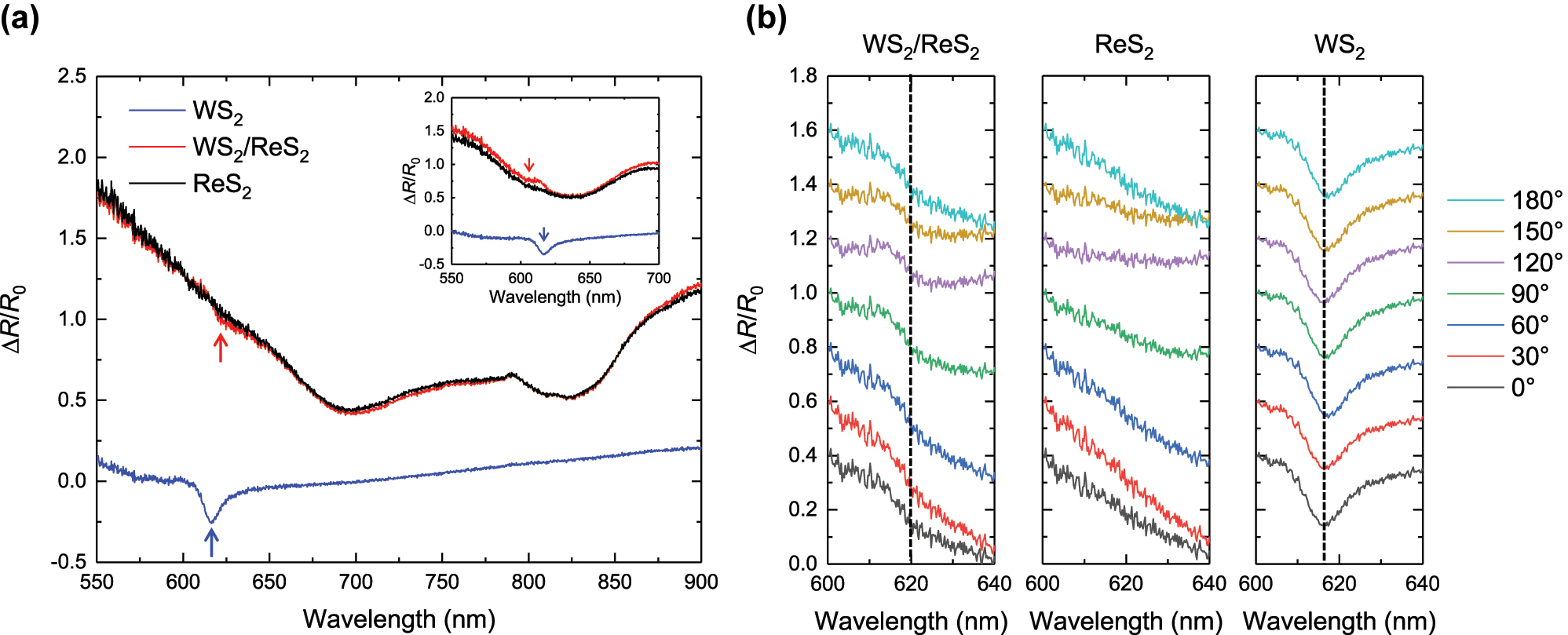
Differential Reflectance Characterization of WS2/ReS2 Heterostructure. (a) Differential reflectance of WS2 (blue), ReS2 (black), and WS2/ReS2 (red) at an excitation angle of 0°. The inset highlights the differential reflectance of each region in the wavelength range of 550–700 nm at an excitation angle of 90°. (b) Excitation angle-dependent differential reflectance spectra of WS2/ReS2, ReS2, and WS2 in the range of WS2 absorption.
From the excitation angle-dependent ΔR/R 0 spectrum in the 600–640 nm range (Figure 2(b)), we observed that the WS2 exciton resonance dip feature at 620 nm displays periodicity at 90° intervals in WS2/ReS2. Notably, at 0°, the WS2 dip closely resembles that of ReS2, whereas at 90°, the dip resembles the dip from isotropic monolayer WS2 of which intrinsic dips lack the excitation angle dependence.
Assuming the dielectric contribution is dominated by the resonances of bound excitons, the broadening of the WS2 dip at 0° is attributed to strong exciton resonance hybridization resulting from crystallographic orientation-dependent dielectric constant of ReS2 as indicated by excitation angle-dependent ΔR/R 0 spectrum (Supplementary Information, 4). Comparing the ΔR/R 0 spectrum at an excitation angle of 90° to that at 0°, we observe a notable difference in the behavior of the WS2/ReS2 heterostructure, as illustrated in Figure 2(a) and its inset. At 0°, the dip in the ΔR/R 0 spectrum of the heterostructure shows a smaller intensity than that of the individual ReS2 layer, indicating enhanced absorption of WS2 excitons. In contrast, at an excitation angle of 90°, the ΔR/R 0 spectrum of ReS2 undergoes a general blue shift of its reflectance dip compared to excitation angle of 0°, leading to the dip of ReS2 in the WS2/ReS2 heterostructure moving closer to that of WS2. This results in an increase in its optical transition energy and a slight blue shift of WS2, along with higher intensity of ΔR/R 0 indicating reduced absorption of WS2 excitons than under excitation at 0°. These observations suggest that the anisotropic dielectric environment of ReS2 significantly influences the WS2 exciton resonance in the heterostructure.
The PL spectra primarily reflect both direct and indirect transitions and are more sensitive to radiative recombination during transitions to the lowest energy state. In contrast, the ΔR/R 0 spectrum, which resonates with direct transitions, provides more comprehensive information about charge transitions. This allows us to uncover the dielectric environment mirroring effect in WS2/ReS2, which is not as apparent in the PL spectra.
To investigate the relationship between the optical anisotropy in temporal behaviors of excitons, we performed time-resolved photoluminescence (TRPL) measurements on WS2/ReS2 and WS2 using a time-correlated single photon counting (TCSPC) system, coupled with the same cross-polarization setup used in PL measurements. A bandpass filter (610 nm ± 10 nm) was placed in the light path of the TCSPC to isolate the radiative recombination of neutral WS2 excitons. In Figure 3(a), we compare the lifetime decay characteristics of WS2 and WS2/ReS2 under an excitation angle of 0°.
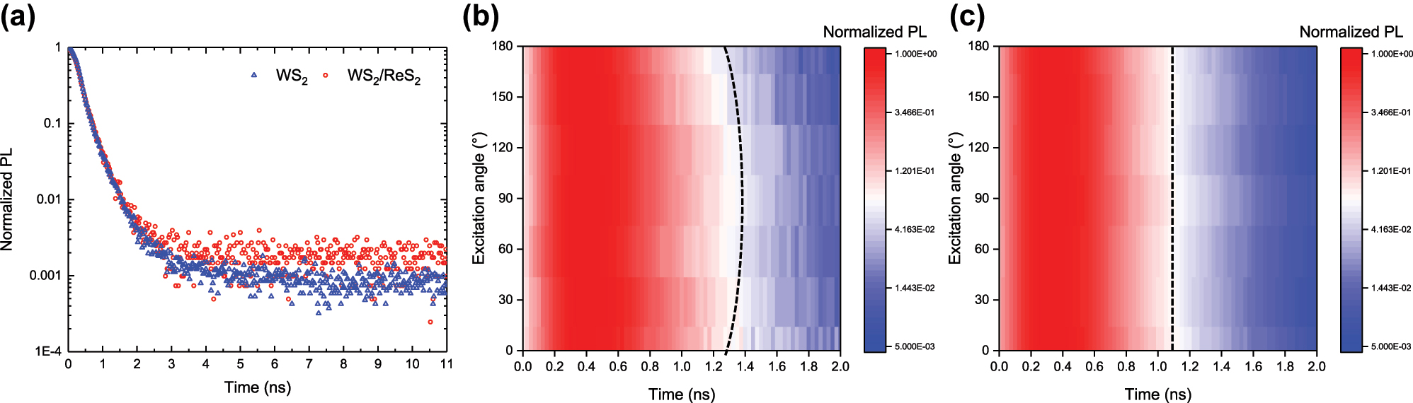
Time-Resolved PL Characterization of WS2/ReS2 Heterostructure. (a) Time-resolved PL decay characteristics in WS2 (blue) and WS2/ReS2 (red) at an excitation angle of 0°. Excitation angle-dependent decay characteristics in (b) WS2/ReS2 and (c) WS2.
To ensure accurate analysis of the decay curve and precise determination of the PL lifetime, the decay curves for each region were normalized to their highest PL intensities and fitted with an exponential decay equation, I = I 0e−t/ τ , to extract the exciton lifetime values, τ. Additionally, the time point where the normalized PL intensity equals to unity was used as the starting point for the decay analysis. The extracted lifetimes were τ WS2/ReS2 = 0.33 ± 0.003 ns, τ WS2 = 0.32 ± 0.004 ns, indicating negligible differences. Interestingly, lifetime decay characteristics at excitation angle of 90° reveal τ WS2/ReS2 increases to 0.38 ± 0.004 ns, in contrast to τ WS2 = 0.32 ± 0.004 ns, as shown in Figure 3(b) and (c) and Supplementary Information, 5. The previously reported PL lifetime of WS2 and transient absorption decay in ReS2/WS2 heterostructures, which were observed to be shorter than those of monolayer WS2 (within the 10–100 ps range) [26], [28], were not evident in our case.
Anisotropic lifetime of WS2 in the heterostructure region can be attributed to band anisotropy in combination with the electron–phonon scattering [40], [41], as well as more efficient charge mobility and exciton diffusion coefficient along the b-axis of ReS2. While more photocarriers are generated along the b-axis compared to the a-axis of ReS2 [40], [42], as indicated by higher PL intensities and absorption at 620 nm at an excitation angle of 0°, the enhanced charge transport efficiency along the b-axis results in faster charge recombination in WS2 on ReS2. Consequently, slightly shorter lifetime is justified to cool hot electrons via electron–phonon coupling along the b-axis. This observation aligns with angle-dependent relaxation times previously reported in SnS and BP, which exhibits optical anisotropy induced by orthorhombic structures [43], [44].
In addition, our observed lifetime anisotropy of WS2 in the WS2/ReS2 heterostructure region is consistent with previous time-resolved photoelectron emission microscopy results for WSe2 on ReS2 under controlled probe polarization [45]. In particular, the strong anisotropy of time constant suggests that interlayer charge transfer process is faster along the b-axis, due to faster evolution of excited electron distribution. The anisotropic lifetime of WS2 in the WS2/ReS2 suggests that the crystal orientation of ReS2 along the a- and b-axes may lead to variations in the band structure, including band dispersion flattening and the electron hopping behaviors [41], which can influence excitonic recombination lifetimes.
Lastly, we analyzed the power-dependent PL anisotropy by tracking the anisotropy parameter (A) defined as (I max − I min)/(I max + I min), as a function of laser power. I max and I min represent the PL peak intensity at 0° and 90°, respectively, with I max showing the maximum intensity at 0° and I min corresponding to the minimum intensity at 90°. First, as shown in Figure 4(a), the PL intensity contrast at different excitation angles increases with higher laser power. Figure 4(b) and (c) present the PL spectra at various laser powers for excitation angles of 0° and 90°, and the corresponding calculated A values, respectively. The anisotropy parameter A increases within the laser power range of 4–15 µW, while at a low power of 2 µW, the PL intensities decrease significantly due to insufficient optical excitation (Supplementary Information, 6 and 7). However, at the highest laser power of 47 µW, anisotropy parameter declines back to values observed in the 4 µW range, which implies the optical anisotropy influenced by optical densities of the photons.
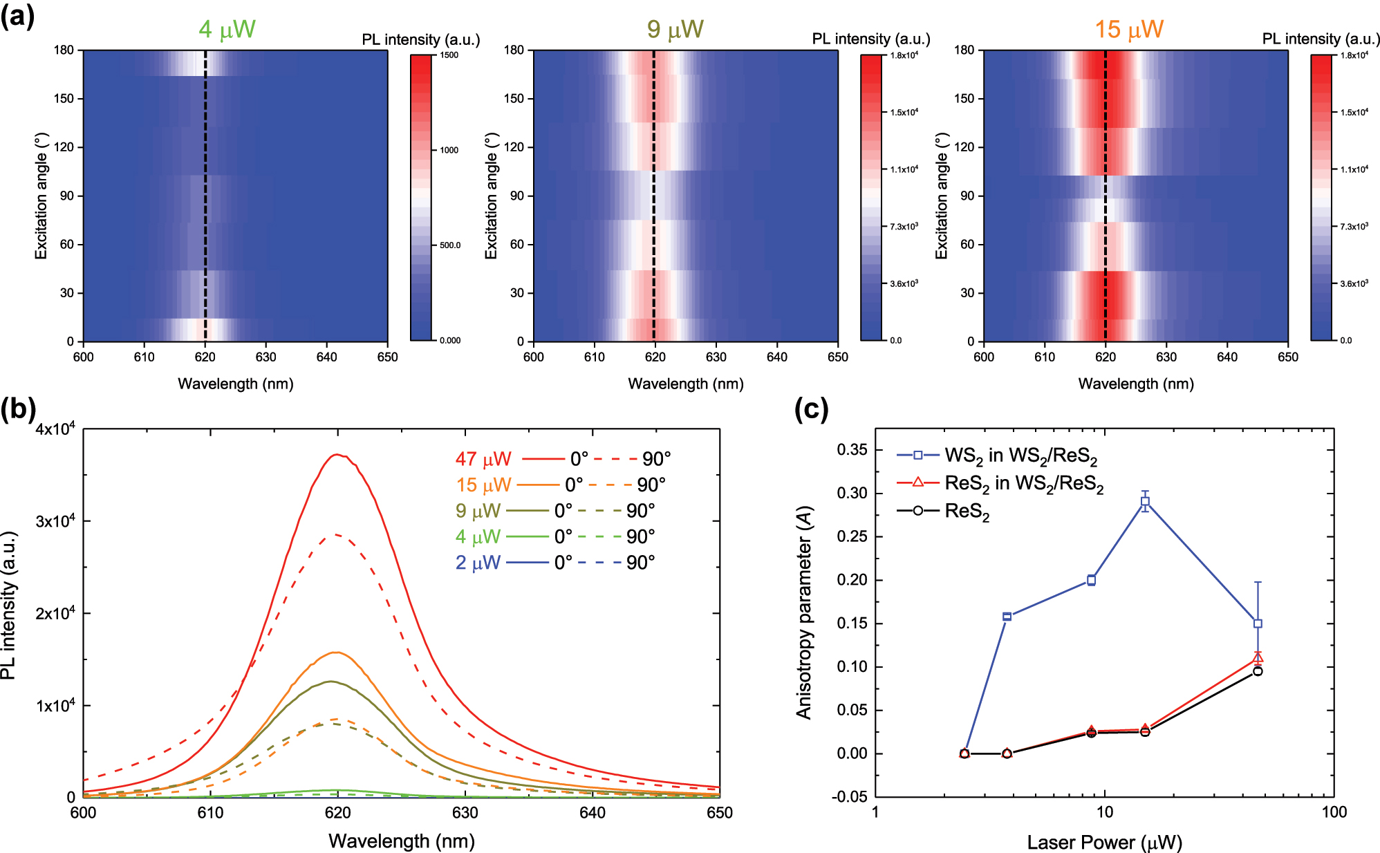
Laser Power-Dependent PL Characterization of WS2/ReS2 Heterostructure. (a) Excitation angle-dependent PL spectra of WS2/ReS2 in the WS2 emission range at laser powers of 4 μW, 9 μW, and 15 μW. (b) Power-dependent PL spectra at excitation angles of 0° and 90°, with laser power varying from 2 μW to 47 μW. (c) Anisotropy parameter of WS2 emission in WS2/ReS2 (blue), ReS2 emission in WS2/ReS2 (red), and ReS2 emission in ReS2 itself (black), as a function of laser power.
The increase in A within the 4–15 µW laser power range can be attributed to not only the greater absorption of incident light enhancing the number of photo-generated carriers but also disparity in the amounts of the photo-generated carriers along the crystallographic axes. Specifically, at higher powers, the abundance of photo-generated carriers along the b-axis with excessive energy enhances wavefunction overlap, facilitating charge transfer from WS2 to ReS2 along the type-II band alignment [26], [28]. This effect is particularly pronounced when optical excitation occurs along the b-axis of ReS2 (0°), where optical oscillator strength is strongest originating from anisotropic electronic band structure. In this case, the effective charge transfer and separation of photocarriers become more significant, leading to stronger interlayer coupling between WS2 and ReS2. This coupling, combined with the inherent anisotropy of ReS2 due to its crystallographic axes, amplifies the optical anisotropy of WS2 at high optical densities.
The enhanced anisotropy of WS2 at high optical densities, resulting from an increased disparity in the amounts of photogenerated carriers depending on the optical excitation direction, is further supported by data in Supplementary Information, 8, where the integrated PL areas at 620 nm and 630 nm are compared. Each wavelength of the PL peak indicates radiative recombination of neutral exciton (620 nm) and trion (630 nm) [33], [37]. At an excitation angle of 0°, the proportion of the 630 nm area is higher at 15 µW than at 4 µW, suggesting an increase in trion population due to a higher optical doping carrier density. Additionally, as the excitation angle changes from 90° to 0°, the integrated area at 630 nm increases, indicating that the radiative recombination path of trions become more prominent due to anisotropically enhanced localizations of photo-generated carriers along the b-axis. The faster decay of WS2 neutral exciton in WS2/ReS2 at an excitation angle of 0° further supports the reduction in the integrated PL area of neutral excitons at the same angle.
On the other hand, the abnormal decrease in anisotropy at 47 µW can be explained by the increased role of electron–phonon coupling due to excessive thermal energy. Under these high power conditions, the trion population no longer increases as it did at 15 µW. Instead, the integrated 630 nm area remains comparable to that observed at 15 μW at excitation angle of 0°. The excessive thermal energy increases the likelihood of charge carriers being excited to higher energy states far from band edges, accompanied by phonon scattering. In heterostructures, enhanced electron–phonon coupling can lead to phonon softening, which induces weakening of interlayer coupling caused by an increased interlayer distance [46], [47], [48]. When the photon density of the laser exceeds the critical range, the increased interlayer distance impedes the efficient wavefunction overlap between the layers [49], [50], causing WS2 on ReS2 to lose its anisotropic optical response.
Furthermore, in contrast to the decrease in the anisotropy parameter of WS2 in the WS2/ReS2 heterostructure at the 47 µW, the anisotropy parameter of ReS2 in the heterostructure and ReS2 itself steadily increases. Therefore, we hypothesize that the anisotropic optical response of WS2, particularly induced by ReS2, arises from optical excitation, which generates photocarriers whose amounts vary with the optical excitation angle. At higher optical densities, disparity in population of localized photogenerated carriers increases, thereby enhancing the optical anisotropy in WS2 on ReS2.
3 Conclusions
In this study, we investigated how an isotropic material, WS2, adjacent to an anisotropic material, ReS2, can exhibit anisotropic optical responses. Through excitation angle-dependent PL, differential reflectance, time-resolved PL, and power-dependent PL anisotropy analyses, we demonstrated that the isotropic emission response of WS2 is influenced by the anisotropic optical properties of ReS2, which has crystallographically low symmetry. By comparing the excitation angle-dependent PL intensities of WS2 on ReS2 with those of individual WS2 and ReS2 layers, we confirmed that the anisotropic optical response of ReS2 modulates the optical behavior of WS2. In differential reflectance measurements, we observed that the anisotropic dielectric environment of ReS2 influences the WS2 exciton resonance. The shorter emission lifetime anisotropy in the WS2/ReS2 under excitation parallel to the b-axis indicates that the efficient charge mobility along the b-axis of ReS2 facilitates faster charge transfer. We identified that anisotropic charge transport originating from band structure anisotropy, along with electron–phonon scattering, should be carefully considered when interpreting the optical and temporal dynamics of WS2 excitons in WS2/ReS2 heterostructure.
The increasing anisotropy at higher optical photon densities suggests that the enhanced population of photo-generated carriers along the b-axis, along with their disparity, plays a key role in optical anisotropy. These results highlight the importance of carefully considering optical excitation, in conjunction with structural anisotropy, when interpreting optical responses in heterostructures consisting of isotropic and anisotropic material. This work provides valuable insights into harnessing anisotropic exciton states for the development of advanced anisotropic optoelectronic and photonic devices by symmetry breaking in 2D materials.
4 Materials and methods
4.1 Fabrication of WS2/ReS2 heterostructure
To assemble the WS2/ReS2 heterostructure, we used mechanical exfoliation and dry transfer. Multilayer ReS2 and monolayer WS2 were exfoliated from their bulk crystals (2D Semiconductors and HQ Graphene) with mechanical exfoliation (the Scotch tape method) onto SiO2/Si substrate and PDMS (Gel-Pak X4), respectively. We prepared WS2 with a cleaved edge along the isotropic crystallographic direction, exhibiting 60° angles at the corners, and ReS2 with a clearly defined b-axis along the anisotropic crystallographic direction. We stacked monolayer WS2 onto multilayer ReS2 on SiO2/Si with aligning the crystal axes, utilizing a rotation stage (Zaber XLSM025A) having an angular accuracy of up to 80 millidegrees (0.08°) to minimize atomic reconstruction between two layers. We used a transfer stage (Newport XYZ-PPP) inside a humidity-controlled glovebox to reduce the effects of adsorbates, contaminants, and oxidation of sample during transfer.
4.2 Optical and topographical characterizations
PL/Raman spectroscopy, differential reflectance spectroscopy, and time-resolved PL measurements were conducted using a customized confocal Raman microscope (NanoBase XPER Raman system) at room temperature. For PL/differential reflectance and Raman measurements, gratings with 300 lines per mm (lpmm) and 1800 lpmm were used, respectively, providing spectral resolutions of 0.9 nm and 4.3 cm−1. For excitation angle-dependent microscopic investigations, a linear polarizer was incorporated in the incident laser path to align the laser polarization direction with the b-axis of ReS2. An analyzer in a cross-polarization configuration was added, and the sample was manually rotated in 30° increments to adjust the excitation angle. Area mapping of optical responses was performed with lower than 1 µm spatial resolution using a galvo-mirror scanner, and area-averaged spectra were extracted to minimize discrepancies caused by surface roughness in single-point spectra.
For PL/Raman spectroscopy, a continuous-wave 532 nm green laser (Cobolt Tor) was used as the excitation source and emitted and scattered light was collected by the detector. Laser power was controlled using a continuous neutral density filter. For reflectance measurements, a broadband halogen lamp (U-LH100L-3) served as the excitation source. The sample was globally illuminated with white light, and the reflectance signal from the target area (selected via a galvo mirror) was collected using a confocal setup with 300 lpmm grating. Charge-coupled device camera (iVac 316, Andor) was employed for detection of PL/Raman and reflectance signals.
TRPL measurements were performed using a time-correlated single photon counting (TCSPC) system, consisting of a single-photon avalanche detector (PDM series, PicoQuant) and time-tagging electronics (TimeHarp 260, PicoQuant) with a timing resolution of 30 ps and 25 ps, respectively. A 510 nm ps pulsed diode laser (PDL 800D, PicoQuant) operating at an 80 MHz repetition rate was used for excitation. To isolate 510 nm excitation light and emission signals from neutral WS2 excitons, a 510 ± 10 nm bandpass filter was placed in the excitation path, and a 610 ± 10 nm bandpass filter was positioned before the detector.
Atomic force microscopy (AFM) (Vista One, Molecular Vista) was used for surface topography imaging and roughness analysis. A gold-coated silicon tip with a <35 nm radius (Q:NSC15/Cr-Au, MikroMasch) was employed for noncontact mode AFM scans. The scanning covered the sample area with a resolution of 512 pixels and a scan speed of 8 μm/s.
Funding source: Directorate for Engineering
Award Identifier / Grant number: CMMI-2135734, CMMI-2306039, ECCS-2201054, and CBET-2035584
Funding source: Air Force Office of Scientific Research
Award Identifier / Grant number: FA2386-21-1-4129 and FA9550-23-1-0134
Funding source: Office of Naval Research
Award Identifier / Grant number: N000142412533
Funding source: National Research Foundation of Korea
Award Identifier / Grant number: RS-2024-00408180
-
Research funding: This research was supported by the AFOSR (FA2386-21-1-4129 and FA9550-23-1-0134), ONR (N000142412533), NSF (CMMI-2135734, CMMI-2306039, ECCS-2201054, and CBET-2035584), and National Research Foundation of Korea (NRF) funded by Ministry of Science and ICT (RS-2024-00408180).
-
Author contributions: All authors have accepted responsibility for the entire content of this manuscript and consented to its submission to the journal, reviewed all the results, and approved the final version of the manuscript. SK, TY, PJM, and SN initiated the research and wrote the manuscript. SK and SN designed the experiments. SK, TY, and PJM conducted all experiments.
-
Conflict of interest: Authors state no conflict of interest.
-
Data availability: The data that support the findings of this study are available from the corresponding author upon reasonable request.
References
[1] K. F. Mak, C. Lee, J. Hone, J. Shan, and T. F. Heinz, “Atomically thin MoS2: a new direct-gap semiconductor,” Phys. Rev. Lett., vol. 105, no. 13, 2010. https://doi.org/10.1103/physrevlett.105.136805.Suche in Google Scholar PubMed
[2] H. R. Gutiérrez, et al.., “Extraordinary room-temperature photoluminescence in triangular WS 2 monolayers,” Nano Lett., vol. 13, no. 8, 2013. https://doi.org/10.1021/nl3026357.Suche in Google Scholar PubMed
[3] D. H. Lien, et al.., “Electrical suppression of all nonradiative recombination pathways in monolayer semiconductors,” Science, vol. 364, no. 6439, 2019. https://doi.org/10.1126/science.aaw8053.Suche in Google Scholar PubMed
[4] H. Kim, S. Z. Uddin, N. Higashitarumizu, E. Rabani, and A. Javey, “Inhibited nonradiative decay at all exciton densities in monolayer semiconductors,” Science, vol. 373, no. 6553, 2021. https://doi.org/10.1126/science.abi9193.Suche in Google Scholar PubMed
[5] D. Xiao, G. Bin Liu, W. Feng, X. Xu, and W. Yao, “Coupled spin and valley physics in monolayers of MoS 2 and other group-VI dichalcogenides,” Phys. Rev. Lett., vol. 108, no. 19, 2012. https://doi.org/10.1103/physrevlett.108.196802.Suche in Google Scholar
[6] H. Zeng, J. Dai, W. Yao, D. Xiao, and X. Cui, “Valley polarization in MoS 2 monolayers by optical pumping,” Nat. Nanotechnol., vol. 7, no. 8, 2012. https://doi.org/10.1038/nnano.2012.95.Suche in Google Scholar PubMed
[7] K. F. Mak, K. He, J. Shan, and T. F. Heinz, “Control of valley polarization in monolayer MoS2 by optical helicity,” Nat. Nanotechnol., vol. 7, no. 8, 2012. https://doi.org/10.1038/nnano.2012.96.Suche in Google Scholar PubMed
[8] T. Cao, et al.., “Valley-selective circular dichroism of monolayer molybdenum disulphide,” Nat. Commun., vol. 3, no. 1, p. 887, 2012. https://doi.org/10.1038/ncomms1882.Suche in Google Scholar PubMed PubMed Central
[9] K. He, et al.., “Tightly bound excitons in monolayer WSe2,” Phys. Rev. Lett., vol. 113, no. 2, 2014. https://doi.org/10.1103/physrevlett.113.026803.Suche in Google Scholar
[10] A. Chernikov, et al.., “Exciton binding energy and nonhydrogenic Rydberg series in monolayer WS2,” Phys. Rev. Lett., vol. 113, no. 7, 2014. https://doi.org/10.1103/physrevlett.113.076802.Suche in Google Scholar
[11] M. Kulig, et al.., “Exciton diffusion and halo effects in monolayer semiconductors,” Phys. Rev. Lett., vol. 120, no. 20, 2018. https://doi.org/10.1103/physrevlett.120.207401.Suche in Google Scholar PubMed
[12] F. Cadiz, et al.., “Exciton diffusion in WSe2 monolayers embedded in a van der Waals heterostructure,” Appl. Phys. Lett., vol. 112, no. 15, 2018, Art. no. 152106. https://doi.org/10.1063/1.5026478.Suche in Google Scholar
[13] K. F. Mak, et al.., “Tightly bound trions in monolayer MoS 2,” Nat. Mater., vol. 12, no. 3, 2013. https://doi.org/10.1038/nmat3505.Suche in Google Scholar PubMed
[14] Y. You, X. X. Zhang, T. C. Berkelbach, M. S. Hybertsen, D. R. Reichman, and T. F. Heinz, “Observation of biexcitons in monolayer WSe 2,” Nat. Phys., vol. 11, no. 6, 2015. https://doi.org/10.1038/nphys3324.Suche in Google Scholar
[15] F. A. Rasmussen and K. S. Thygesen, “Computational 2D materials database: electronic structure of transition-metal dichalcogenides and oxides,” J. Phys. Chem. C, vol. 119, no. 23, 2015. https://doi.org/10.1021/acs.jpcc.5b02950.Suche in Google Scholar
[16] G. P. Neupane, K. Zhou, S. Chen, T. Yildirim, P. Zhang, and Y. Lu, “In-Plane Isotropic/Anisotropic 2D van der Waals Heterostructures for Future Devices,” Small, vol. 15, no. 11, 2019. https://doi.org/10.1002/smll.201804733.Suche in Google Scholar PubMed
[17] H. Liu, et al.., “Phosphorene: an unexplored 2D semiconductor with a high hole mobility,” ACS Nano, vol. 8, no. 4, 2014. https://doi.org/10.1021/nn501226z.Suche in Google Scholar PubMed
[18] L. C. Gomes and A. Carvalho, “Phosphorene analogues: isoelectronic two-dimensional group-IV monochalcogenides with orthorhombic structure,” Phys. Rev. B:Condens. Matter Mater. Phys., vol. 92, no. 8, 2015. https://doi.org/10.1103/physrevb.92.085406.Suche in Google Scholar
[19] A. Favron, et al.., “Photooxidation and quantum confinement effects in exfoliated black phosphorus,” Nat. Mater., vol. 14, no. 8, 2015. https://doi.org/10.1038/nmat4299.Suche in Google Scholar PubMed
[20] A. S. Sarkar and E. Stratakis, “Recent advances in 2D metal monochalcogenides,” Advanced Science, vol. 7, no. 21, 2020. https://doi.org/10.1002/advs.202001655.Suche in Google Scholar PubMed PubMed Central
[21] Y. C. Lin, et al.., “Single-layer ReS2: two-dimensional semiconductor with tunable in-plane anisotropy,” ACS Nano, vol. 9, no. 11, 2015. https://doi.org/10.1021/acsnano.5b04851.Suche in Google Scholar PubMed
[22] D. A. Chenet, et al.., “In-plane anisotropy in mono- and few-layer ReS2 probed by Raman spectroscopy and scanning transmission electron microscopy,” Nano Lett., vol. 15, no. 9, 2015. https://doi.org/10.1021/acs.nanolett.5b00910.Suche in Google Scholar PubMed
[23] Y. Jiang, S. Chen, W. Zheng, B. Zheng, and A. Pan, “Interlayer exciton formation, relaxation, and transport in TMD van der Waals heterostructures,” Light: Sci. Appl., vol. 10, no. 1, 2021. https://doi.org/10.1038/s41377-021-00500-1.Suche in Google Scholar PubMed PubMed Central
[24] A. Varghese, et al.., “Near-direct bandgap WSe2/ReS2 type-II pn heterojunction for enhanced ultrafast photodetection and high-performance photovoltaics,” Nano Lett., vol. 20, no. 3, 2020. https://doi.org/10.1021/acs.nanolett.9b04879.Suche in Google Scholar PubMed
[25] D. Liu, et al.., “Synthesis of 2H-1T′ WS2-ReS2 heterophase structures with atomically sharp interface via hydrogen-triggered one-pot growth,” Adv. Funct. Mater., vol. 30, no. 16, 2020. https://doi.org/10.1002/adfm.201910169.Suche in Google Scholar
[26] Y. Tang, et al.., “Distinctive interfacial charge behavior and versatile photoresponse performance in isotropic/anisotropic WS2/ReS2Heterojunctions,” ACS Appl. Mater. Interfaces, vol. 12, no. 47, 2020. https://doi.org/10.1021/acsami.0c14886.Suche in Google Scholar PubMed
[27] M. Zhao, et al.., “Interlayer coupling in anisotropic/isotropic van der Waals heterostructures of ReS2 and MoS2 monolayers,” Nano Res., vol. 9, no. 12, 2016. https://doi.org/10.1007/s12274-016-1247-y.Suche in Google Scholar
[28] F. Huang, et al.., “Controllable resistive switching in ReS2/WS2 heterostructure for nonvolatile memory and synaptic simulation,” Advanced Science, vol. 10, no. 28, 2023. https://doi.org/10.1002/advs.202302813.Suche in Google Scholar PubMed PubMed Central
[29] A. Karmakar, et al.., “Dominating interlayer resonant energy transfer in type-II 2D heterostructure,” ACS Nano, vol. 16, no. 3, 2022. https://doi.org/10.1021/acsnano.1c08798.Suche in Google Scholar PubMed
[30] P. Zereshki, P. Yao, D. He, Y. Wang, and H. Zhao, “Interlayer charge transfer in ReS2/WS2 van der Waals heterostructures,” Phys. Rev. B, vol. 99, no. 19, 2019. https://doi.org/10.1103/physrevb.99.195438.Suche in Google Scholar
[31] N. B. Mohamed, et al.., “Photoluminescence quantum yields for atomically thin-layered ReS2: identification of indirect-bandgap semiconductors,” Appl. Phys. Lett., vol. 113, no. 12, 2018. https://doi.org/10.1063/1.5037116.Suche in Google Scholar
[32] H. X. Zhong, S. Gao, J. J. Shi, and L. Yang, “Quasiparticle band gaps, excitonic effects, and anisotropic optical properties of the monolayer distorted 1T diamond-chain structures ReS2 and ReSe2,” Phys. Rev. B:Condens. Matter Mater. Phys., vol. 92, no. 11, 2015. https://doi.org/10.1103/physrevb.92.115438.Suche in Google Scholar
[33] A. Usman, et al.., “Enhanced excitonic features in an anisotropic ReS2/WSe2 heterostructure,” Nanoscale, vol. 14, no. 30, 2022. https://doi.org/10.1039/d2nr01973f.Suche in Google Scholar PubMed
[34] X. Xie, et al.., “Anisotropic optical characteristics of WS2/ReS2 heterostructures with broken rotational symmetry,” Appl. Phys. Lett., vol. 123, no. 22, 2023. https://doi.org/10.1063/5.0170276.Suche in Google Scholar
[35] H. Zeng, et al.., “Optical signature of symmetry variations and spin-valley coupling in atomically thin tungsten dichalcogenides,” Sci. Rep., vol. 3, no. 1, p. 1608, 2013. https://doi.org/10.1038/srep01608.Suche in Google Scholar PubMed PubMed Central
[36] Y. Luo, W. Su, F. Chen, K. Wu, Y. Zeng, and H. W. Lu, “Observation of strong anisotropic interlayer excitons,” ACS Appl. Mater. Interfaces, vol. 15, no. 47, 2023. https://doi.org/10.1021/acsami.3c12429.Suche in Google Scholar PubMed
[37] G. Plechinger, et al.., “Identification of excitons, trions and biexcitons in single-layer WS2,” Phys. Status Solidi – Rapid Res. Lett., vol. 9, no. 8, 2015. https://doi.org/10.1002/pssr.201510224.Suche in Google Scholar
[38] A. Dhara, et al.., “Additional excitonic features and momentum-dark states in ReS2,” Phys. Rev. B, vol. 102, no. 16, 2020. https://doi.org/10.1103/physrevb.102.161404.Suche in Google Scholar
[39] J. Binder, et al.., “Upconverted electroluminescence via Auger scattering of interlayer excitons in van der Waals heterostructures,” Nat. Commun., vol. 10, no. 1, 2019. https://doi.org/10.1038/s41467-019-10323-9.Suche in Google Scholar PubMed PubMed Central
[40] D. Li, et al.., “Giant transport anisotropy in revealed via nanoscale conducting-path control,” Phys. Rev. Lett., vol. 127, no. 13, 2021. https://doi.org/10.1103/physrevlett.127.136803.Suche in Google Scholar PubMed
[41] D. Biswas, et al.., “Narrow-band anisotropic electronic structure of ReS2,” Phys. Rev. B, vol. 96, no. 8, 2017. https://doi.org/10.1103/physrevb.96.085205.Suche in Google Scholar
[42] Q. Cui, et al.., “Transient absorption measurements on anisotropic monolayer ReS2,” Small, vol. 11, no. 41, 2015. https://doi.org/10.1002/smll.201501668.Suche in Google Scholar PubMed
[43] S. Ge, et al.., “Dynamical evolution of anisotropic response in black phosphorus under ultrafast photoexcitation,” Nano Lett., vol. 15, no. 7, 2015. https://doi.org/10.1021/acs.nanolett.5b01409.Suche in Google Scholar PubMed
[44] K. Sun, et al.., “Dynamical response of nonlinear optical anisotropy in a tin sulfide crystal under ultrafast photoexcitation,” J. Phys. Chem. Lett., vol. 13, no. 40, 2022. https://doi.org/10.1021/acs.jpclett.2c02443.Suche in Google Scholar PubMed
[45] Y. Qin, et al.., “Ultrafast electronic dynamics in anisotropic indirect interlayer excitonic states of monolayer WSe2/ReS2 heterojunctions,” Nano Lett., vol. 23, no. 18, pp. 8643–8649, 2023. https://doi.org/10.1021/acs.nanolett.3c02488.Suche in Google Scholar PubMed
[46] X. Ling, et al.., “Anisotropic electron-photon and electron-phonon interactions in black phosphorus,” Nano Lett., vol. 16, no. 4, p. 2260, 2016. https://doi.org/10.1021/acs.nanolett.5b04540.Suche in Google Scholar PubMed
[47] S. Sinha, S. K. Arora, H. C. Wu, and V. G. Sathe, “Phonon scattering mechanism in van der Waals heterostructures comprising of MoS2 and WS2 nanosheets,” Mater. Today: Proc., vol. 45, pp. 4612–4618, 2021. https://doi.org/10.1016/j.matpr.2021.01.016.Suche in Google Scholar
[48] T. Goo, et al.., “Characterization of polarization-And power-dependent excitons and trions in bulk ReS2,” Appl. Phys. Lett., vol. 121, no. 6, p. 062103, 2022. https://doi.org/10.1063/5.0101951.Suche in Google Scholar
[49] O. Garrity, T. Brumme, A. Bergmann, T. Korn, P. Kusch, and S. Reich, “Interlayer exciton-phonon coupling in MoSe2/WSe2 heterostructures,” Nano Lett., vol. 24, no. 38, p. 11853, 2024. https://doi.org/10.1021/acs.nanolett.4c02757.Suche in Google Scholar PubMed PubMed Central
[50] R. Reho, A. R. Botello-Méndez, D. Sangalli, M. J. Verstraete, and Z. Zanolli, “Excitonic response in transition metal dichalcogenide heterostructures from first-principles: Impact of stacking, twisting, and interlayer distance,” Phys. Rev. B, vol. 110, no. 3, p. 035118, 2024. https://doi.org/10.1103/PhysRevB.110.035118.Suche in Google Scholar
Supplementary Material
This article contains supplementary material (https://doi.org/10.1515/nanoph-2024-0672).
© 2025 the author(s), published by De Gruyter, Berlin/Boston
This work is licensed under the Creative Commons Attribution 4.0 International License.
Artikel in diesem Heft
- Frontmatter
- Editorial
- Emerging phenomena in nanophotonics
- Reviews
- Programmable photonic unitary circuits for light computing
- Exploring the frontier: nonlinear optics in low dimensional materials
- Emergent 2D van der Waals materials photonic sources
- Stimulated Brillouin scattering in micro/nanophotonic waveguides and resonators
- Perspective
- Deterministic generation and nanophotonic integration of 2D quantum emitters for advanced quantum photonic functionalities
- Letter
- Harnessing in-plane optical anisotropy in WS2 through ReS2 crystal
- Research Articles
- Frequency-comb-referenced multiwavelength interferometry for high-precision and high-speed 3D measurement in heterogeneous semiconductor packaging
- Nanoscale heat generation in a single Si nanowire
- Visible transparency modulated cooling windows using pseudorandom dielectric multilayers
- W-band frequency selective digital metasurface using active learning-based binary optimization
- Electrodynamics of photo-carriers in multiferroic Eu0.75Y0.25MnO3
- Polarization-independent narrowband photodetection with plasmon-induced thermoelectric effect in a hexagonal array of Au nanoholes
- All-optical switch exploiting Fano resonance and subwavelength light confinement
- Efficient non-Hermitian wave-modulation protocol with a rapid parametric jump
- Colloidal-quantum-dot nanolaser oscillating at a bound-state-in-the-continuum with planar surface topography for a high Q-factor
- On-chip manipulation of trion drift in suspended WS2 monolayer at room temperature
- Resonance modes in microstructured photonic waveguides: efficient and accurate computation based on AAA rational approximation
- Dielectric permittivity extraction of MoS2 nanoribbons using THz nanoscopy