All-optical switch exploiting Fano resonance and subwavelength light confinement
-
Quentin Saudan


Abstract
We propose and experimentally demonstrate a small-mode volume bowtie cavity design for all-optical switching applications using a waveguide-cavity structure that exploits asymmetric Fano resonance lineshapes. The bowtie cavity has a mode volume that is five times smaller than conventional (H0-type) photonic crystal point-defect cavities enabling higher nonlinearity and faster switching. Blue and red-detuned Fano resonant devices based on bowtie cavity designs have been fabricated and characterized. Measured linear transmission spectra have been compared to coupled-mode theory models to extract key parameters such as Q-factors. Furthermore, all-optical switching at 2.5 Gbps have been demonstrated in a wavelength-conversion experiment.
1 Introduction
Optical cavities that strongly enhance light–matter interaction have enabled realization of several all-optical signal processing devices and applications including optical memory [1], optical switches [2], [3], [4], [5], optical diodes [6], [7], narrow-band filters [8], and semicondutor nanolasers [9], [10], [11], [12]. Point-defect cavities using photonic bandgap effects to confine light enable the realization of cavities with high quality factor and, simultaneously, small optical mode volume [13], [14]. Conventional point-defect cavities have mode volumes on the order of ≃2V λ or larger, where V λ ≡ (λ/2n)3, with n the refractive index of the material, and λ the wavelength of light. Here, V λ is often denoted the diffraction-limited mode volume for dielectric cavities [15], although several designs [16], [17], [18] and recent experimental results [19], [20], [21] show that mode volumes much smaller than V λ can be achieved. For optical switching, a smaller mode volume implies a stronger spatial concentration of light, enabling more efficient and faster switching. In particular, indium phosphide (InP) based photonic crystal membranes constitute an important platform for realizing such nanocavities and integrating them with active material and passive waveguides [22]. Additionally, InP is suitable for generating free-carriers using two-photon absorption with photon energies in the telecommunication wavelength range.
Optical signal processing functionalities have been improved by tailoring the lineshape of the optical resonance, so that the transmission through the structure is more sensitive towards shifts of the resonance [23]. The resonance is shifted due to the refractive index change induced by the optical pump (control) signal and depends on the particular physical mechanism at play in the material used. However, as pointed out in Ref. [24], the material used has less influence on the required power for switching than the resonant or travelling wave scheme used to enhance the interaction time between light and matter. Two of the commonly used characteristic lineshapes are the Lorentzian and the Fano lineshapes. In particular, the use of asymmetric Fano resonances have enabled improved optical switching characteristics [25]. Fano resonances are a manifestation of wave interference and arise in many different physical systems where a continuum of modes interacts with a discrete resonance [26]. Photonics offers a very rich platform, where Fano resonances has been explored in many different materials and configurations [27], [28], [29], [30].
Figure 1(a) shows a schematic diagram of the Fano structure we are considering. It consists of a nanocavity that is side-coupled to an optical waveguide. A partially transmitting element (PTE) placed in the middle of the waveguide determines whether the lineshape of the transmission spectrum from input to output is symmetric or asymmetric [31]. An asymmetric lineshape indicates the presence of paths of constructive and destructive interference between the discrete state and the continuum of states, depending on the wavelength, cf. Figure 1(b). All-optical switching devices rely on optically shifting the resonance using a control (or pump) optical pulse, which in turn changes the transmission of an optical signal (or probe) pulse. The pump signal generates free-carriers inside the nanocavity through two-photon absorption. The build-up of carriers inside the nanocavity changes the refractive index via the plasma effect, which in turn shifts the resonance wavelength of the nanocavity, thereby changing the transmission of the probe signal [32]. Figure 1(b) illustrates such a resonance shift (Δλ), in which the spectral locations of the pump and the probe signals are indicated by red-shaded and blue-shaded regions, respectively. A comprehensive review on the use of photonic crystal Fano resonances for in-plane optical signal processing applications may be found in Ref. [25].

Device and transmission characteristic. (a) Schematic diagram of a Fano structure consisting of a nanocavity side-coupled to an optical waveguide. A partially transmitting element (PTE) is placed in the middle of the waveguide. (b) Illustration of all-optical switching using an asymmetric Fano resonance. The transmission spectrum from input to output, calculated using temporal-coupled-mode theory, are shown for the unshifted resonance (solid line) and the shifted resonance (dashed line). The spectral locations of the probe and pump signals are indicated by the blue and red shaded regions, respectively. (c) Schematic diagram of an integrated photonic crystal Fano device. Light is coupled in and out of the device using grating-assisted fiber-to-chip couplers. The waveguide and nanocavity shown in (a) are implemented in the photonic crystal membrane using a line-defect waveguide and a point-defect cavity.
Several challenges have to be overcome before these all-optical switches can be applied in communication systems. One of these is the cross-talk between the switching and the switched signals, i.e., the pump and probe signals. As the probe and pump signals are in close spectral proximity, the probe signal suffers from in-band cross-talk. This issue can be addressed using multi-mode cavities [33], or photonic molecules [34], [35]. Another issue relates to the requirement that the pump-induced transmission change must relax back to the initial state before the next pump pulse arrives in order to avoid patterning effects [36]. The maximum operation speed of all-optical switches relying on index changes induced by free carriers is thus limited by the rate of carrier recombination. Several approaches have been proposed to increase the switching speed, such as employing a pn-junction in the nanocavity to sweep-out the free-carriers by applying a static electric field [37], and using doped semiconductors to increase the non-radiative recombination rate [4].
Recently, a new class of topolology-optimized nanocavities, denoted extreme dielectric confinement (EDC) cavities, which allow photon confinement well below the diffraction limit in dielectrics has been experimentally demonstrated [21], [38]. The optimal structures have a bowtie structure at the center, which act to concentrate the field due to the boundary conditions of Maxwell’s equations [39]. It was shown theoretically that such nanocavities may speed up the recovery dynamics significantly by relying on fast diffusion of the strongly localized carrier distribution [40]. Other designs employing super-cell tailoring also allow for strong spatial localization of the optical intensity but at multiple hot-spots [41], which is not suitable for switching.
In this paper, we present the design of a bowtie cavity incorporated inside a standard photonic crystal point-defect cavity, which is side-coupled to a line-defect photonic crystal waveguide forming a Fano resonance structure. This design allows simultaneously exploiting the strong light concentration in the bowtie cavity and the Fano resonance to improve the optical switching characteristics. The strong light concentration in the bowtie cavity thus increases the effective nonlinear index change induced by the pump signal and the asymmetric Fano spectrum increases the transmission change of the probe due to the nonlinear index change. The paper reports the first proof-of-principle investigations of such structures, including design optimization, experimental fabrication, linear device characterization, and a system experiment demonstrating wavelength conversion.
2 Bowtie cavity design
A design for a bowtie photonic crystal (PhC) nanocavity of H1 type with an embedded bowtie structure at its center is shown in Figure 2(a). Such a quasi-H1 type cavity is formed by replacing the center airhole with a bowtie structure. The design goal is to focus the H1 dipole mode into a mode with high electric field at the center of the bowtie. This cavity is designed for small-mode volume and high-quality factor using a two-step particle swarm optimization [42] relying on 3D finite difference time domain (FDTD) simulations. First, the bowtie structure is placed at the center of an H1 cavity, i.e., with one missing airhole, and the neighboring airholes were not scaled or shifted. The free parameters for the particle swarm optimization are the bowtie tip radius, the total radius of the bowtie, and the angle of the bowtie. We set the minimum values for the gap and the radius of curvature of the bowtie tip to be 30 nm and 20 nm, respectively. Although smaller tip radius would yield a smaller mode volume, it would not be feasible in our fabrication process based on electron beam lithography. A thorough explanation of the process flow is available in Ref. [43]. A small tip radius would also lead to a confinement of the major part of the field at the surface of the tip, which is undesirable due to scattering [19]. The figure of merit for this first optimization is the mode volume of the cavity evaluated at the center of the bowtie, and the spectral location of the resonance wavelength. After the first optimization, the following parameters are chosen: bowtie radius of curvature of r edge = 25 nm, the gap between the bowtie 30 nm, the radius of curvature of the tip r tip = 22 nm, the angle of the bowtie θ = 37°, and the total radius of the bowtie r bt = 168 nm, cf. Figure 2(b).

Design of bowtie cavity based on the photonic crystal membrane platform. (a) Point-defect H1 cavity with a bowtie at its center. The nearby holes are shifted to optimize the cavity mode, as indicated by C1 (black arrows), C2x (red arrows) and C2y (blue arrows), and their radii are scaled up or down to R1 and R2. (b) The central bowtie structure with identification of key parameters, such as bowtie tip radius, total radius of the bowtie, and the angle of the bowtie.
The second optimization is performed on the H1 cavity with fixed bowtie structure designed in step one. In this case, the free-parameters for the particle swarm optimization are C1, C2x, C2y, R1 and R2 as shown in Figure 2(a). The lattice parameter a and the global airhole radius r of the photonic crystal are also considered as free parameters. The figure-of-merit to be maximized is the ratio of the intrinsic quality factor to the effective mode volume, Q in/V eff, subject to the condition that the resonance wavelength is located in the telecom C-band wavelength range. The final optimized parameters are a PhC lattice constant of a = 522 nm, radius r = 159 nm, C1 = 0.077a, C2x = 0.041a, C2y = 0.065a, R1 = 155 nm, and R2 = 170 nm.
Figure 3(a) shows the spectrum of the cavity field, obtained by 3D finite-difference-time-domain (FDTD) simulations, from which a number of modes can be identified. The modes around 1,550 nm have magnetic field profiles that match the two dipole modes of the H1 cavity, as illustrated in the bottom plots of Figure 3(b), which show the magnetic field-component H z , i.e., in the direction orthogonal to the membrane plane. Looking at the electric field profiles, we see that the dipole mode at 1,553.4 nm has a strongly enhanced electric field at the center of the cavity due to the bowtie structure, whereas the dipole mode at 1,524.1 nm is located at the edges of the bowtie. Hence, we refer to these modes as the bowtie mode and the edge mode, respectively. For comparison, we have plotted the field distributions of the fundamental mode of an H0 type cavity in Figure 3(c). Mentioned in numerous studies on photonic crystal cavities [1], [7], [32], the H0 cavity is the main comparative design helping us to benchmark our newly designed bowtie cavity.

Simulated spectrum and mode profiles. (a) Optical spectrum of the field in the cavity obtained by 3D FDTD simulations. The electric field intensity |E|2 (top panels), and the real part of the magnetic field H z (bottom panels) distributions for: (b) edge mode at 1,524.1 nm and bowtie mode at 1,553.4 nm of the bowtie cavity based on H1 cavity, and (c) the fundamental mode of an H0 cavity for comparison purpose.
The bowtie mode has a quality factor of Q in = 5 × 10⁴, an effective mode volume of V eff = 0.057(λ/n)3 (evaluated at the center of the bowtie cavity), and a nonlinear mode volume [44] of V TPA = 0.723(λ/n)3. Compared to the fundamental mode of an H0 cavity, the bowtie cavity embedded in an H1 cavity has a mode volume that is five times smaller. Although, the intrinsic quality factor of the bowtie mode is four times smaller than the H0 cavity, it will not drastically impact the performance of the Fano resonance device as the total Q-factor, Q tot, will be dominated by the waveguide that it is coupled to. Simulations based on temporal coupled-mode theory (TCMT) model, discussed in ref. [26], [31], [45], suggest that a drop of the Q in from 2 × 10⁵ to 5 × 10⁴, for a fixed waveguide Q-factor Q wg = 1,600, would only result in a reduction of the Q tot from 1,587 to 1,550, and a decrease of the extinction ratio (defined as the ratio of transmission maximum to transmission minimum of the Fano resonance) from 55 dB to 42 dB. Therefore, the impact of a low Q in value is not expected to be significant for the overall performance of the optical switch.
Using the electric field profile of the optimized bowtie design, we calculated the spatial profile of free carriers generated by two-photon absorption. Subsequently, the dynamics of the carrier distribution due to drift and diffusion was simulated using the finite element method from the COMSOL semiconductor module and the results were compared to a reference H0 cavity design. We considered an InP membrane with a slight n-type background doping of 1015 cm−3. The carrier generation rate is adjusted so that the peak carrier concentrations N eff of the two cavities are the same. As expected from the reduction of the mode volume, a shortening of the relaxation tail for the bowtie mode compared to the H0 cavity mode is obtained. This is seen in Figure 4 both in the absence of surface recombination and for a recombination velocity of 105 cm/s. We notice that for the H0 cavity, the initial fast relaxation dynamics is unaffected by the surface recombination velocity, which is not the case for the bowtie mode. As both cavities have the same vertical dimension and surface recombination at the membrane interface, the difference must come from the surface recombination due to the photonic crystal airholes. Hence, we attribute it to the larger exposure of the bowtie mode to air–dielectric interfaces as compared to the H0 cavity mode. On the one hand, this greatly shortens the relaxation tail of the bowtie mode, reducing patterning effects and allowing for a higher modulation speeds. On the other hand, the recombination of carriers at the surface occurs by the capture of electrons in trap states with lower energy, thereby releasing phonons [46] and increasing the temperature.

Carrier density dynamics. (a) The evolution of the effective electron carrier density N eff for the fundamental mode of an H0 cavity (solid lines) and for the bowtie mode of the H1 bowtie cavity (dashed lines) for different surface velocity recombination v s . (b) Zoom-in of the dynamics during the first 5 ps.
3 Bowtie cavity side-coupled to a waveguide
In this section, the H1 bowtie cavity is side-coupled to a photonic crystal waveguide for coupling light in and out of the structure and simultaneously realize an asymmetric Fano resonance that improves the swicthing contrast. As explained in Ref. [25], the interference between the continuum of modes in the waveguide and the discrete mode of a side-coupled nanocavity leads to a Fano resonance. The frequency-dependent transmission through the structure displays the typical characteristics of a Fano resonance, where, in particular, the asymmetry can be controlled through the incorporation a partially transmitting element in the waveguide [25], [31]. Two changes were made to the cavity-waveguide structure of the H1 bowtie cavity compared to the H0 cavity. The first one is bringing the waveguide closer to the cavity, hence increasing the spatial overlap between the waveguide and the cavity modes. The second one is the angular orientation of the bowtie cavity. The bowtie mode has an evanescent field oriented at 30° angle compared to the x-axis of the cavity, as shown in Figure 5(a) by the dashed arrows. Since an efficient interaction between the cavity and the waveguide modes requires a good spatial overlap, a 60° rotation of the bowtie cavity is implemented to improve the coupling [47]. As shown in Figure 5(b), the lower tail of the evanescent field is now vertically oriented, ensuring good overlap with a parallel waveguide. The choice of the rotation angle is fixed by the 60° rotational symmetry of the photonic crystal. We noticed that the coupling between the bowtie mode and the waveguide is very weak for the non-rotated case, leading to very small extinction ratio of the transmission spectrum shown in Figure 5(c).
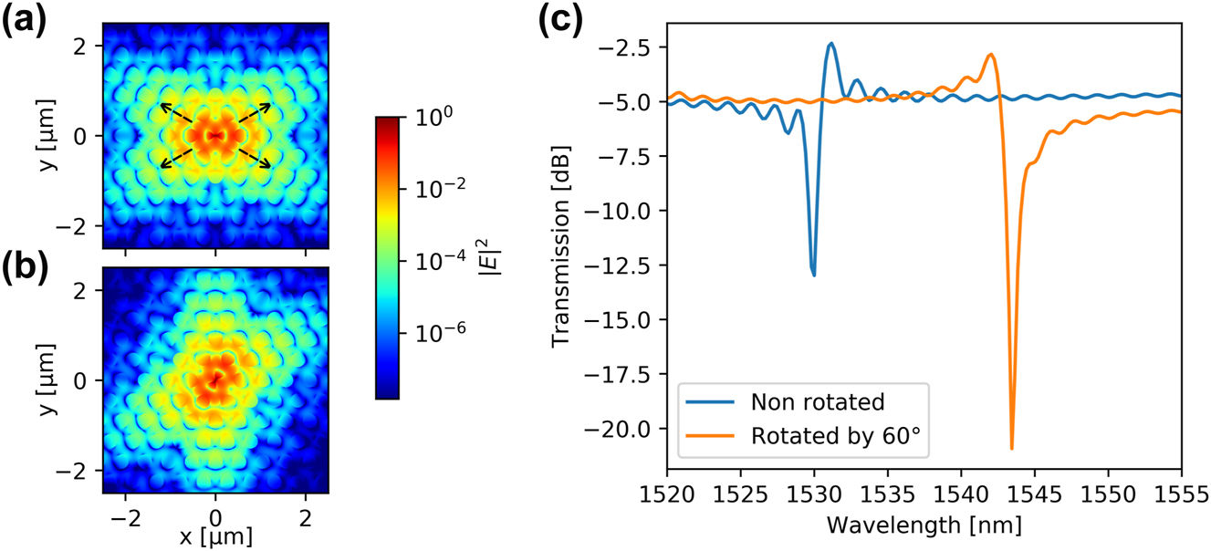
Electric field profile |E|2 for the bowtie mode in logarithmic scale for (a) non-rotated cavity, and (b) cavity rotated by 60°. The dashed arrows indicate the direction of the lobes of the mode field (c) simulated transmission of a device with rotated and non-rotated cavity.
The final design is chosen with a rotation of the bowtie by 60°, and a spacing of 2 photonic crystal rows between the center of the bowtie and the center of the waveguide. The SEM pictures shown as Figure 6(e) and (f) illustrate this design choice as well as the specific placement of the PTE in the waveguide leading to blue- or red-detuned resonances. Indeed, by positioning the PTE symmetrically or anti-symmetrically with respect to the vertical axis of the H1 cavity, the phase of the coupling constant between the cavity and the waveguide is changed and lead to a different Fano resonance [48]. The respective lineshapes are simulated using FDTD and shown in Figure 6(a) and (b), for the blue and red-detuned resonances, respectively. Using TCMT, the simulated transmission spectrum is fitted by taking into account the waveguide transmission as well as the wavelength dependent scattering of the PTE. We thus extract total quality-factor values, Q tot, of 726 and 1,250, and intrinsic quality factors, Q in, of 1,610 and 5,977 for the blue- and red-detuned resonances, respectively. A drastic drop of the intrinsic quality factor is observed between the value calculated through the field relaxation in the intrinsic cavity shown in Figure 3, and the value extracted from the fitting of the transmission lineshape. This deterioration of Q in, and the extinction ratio, is due to the addition of the waveguide in close proximity of the cavity, which modifies its resonant properties. In the case of the H0 cavity, the waveguide is typically placed 3 photonic crystal rows from the cavity, leading to a much smaller perturbation. Despite these slightly low extinction ratios of the current designs, we proceed to the fabrication of the devices with H1 bowtie cavities. The fabrication of the devices follows a procedure similar to the one we reported earlier in Ref. [43].
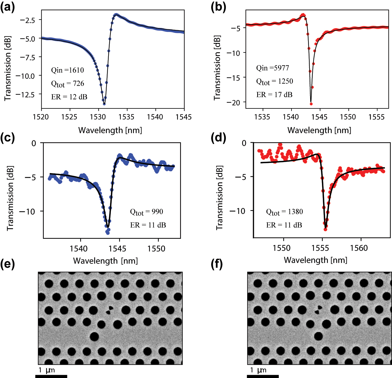
Simulated linear transmission of the H1 bowtie device side-coupled with a waveguide exhibiting (a) blue-detuned and (b) red-detuned asymmetric Fano lineshapes. The blue/red dots show FDTD simulation results, whereas the black solid line shows the prediction of temporal-coupled-mode theory using the fitted parameter values given in the figures. Measured transmission spectrum of (c) blue-detuned, and (d) red-detuned H1 bowtie devices obtained using a Santec-550 tunable laser source. The solid line is the result obtained by fitting to temporal-coupled-mode theory with the indicated parameters. Scanning electron microscope (SEM) images of the fabricated (e) blue-detuned, and (f) red-detuned photonic crystal Fano structures based on bowtie cavities.
We observe asymmetric Fano lineshapes in the linear transmission measurements as shown in Figure 6(c) and (d). We find that cavities with designed hole radius of 133 nm are spectrally located in the C-band. We observe extinction ratios of
4 All-optical switching characterization
To investigate the dynamical switching properties of the fabricated structures, wavelength conversion experiments are carried out. Figure 7(a) shows the schematic diagram of the experimental setup. Light from a mode-locked laser (MLL), centered around 1,545 nm at 10 GHz repetition rate, is amplified using an erbium-doped fiber amplifier (EDFA) and then launched into a 400 m long highly nonlinear fiber (HNLF) for generating a supercontinuum of light covering the entire C-band. A wavelength-selective switch (WSS) is then used to spectrally carve out the optical spectrum of the pump signal, which is positioned around the peak of the Fano resonance. A pseudo-random bit sequence from a bit-pattern generator (BPG) is used as modulating input signal to a Mach–Zehnder intensity modulator (MZM) to generate a train of on-off keying modulated pump pulses. A continuous wave (CW) tunable laser source (TLS) is used to generate a probe signal spectrally located around the minimum transmission of the Fano resonance. The pump and probe signals are polarization controlled and combined using a 3 − dB coupler before being coupled to the device under test (DUT). Here, the blue-detuned bowtie cavity based Fano resonance of Figure 6(c) is used as the DUT. After the DUT, an optical tunable filter (OTF) is used to filter-out the pump signal. The resulting wavelength-converted signal is detected using a photodiode, and analysed using a digital communication analyser (DCA), and an error analyser (EA). A variable optical attenuator (VOA) is used to control the power of the signal arriving at the photodiode.

Wavelength conversion. (a) Schematic diagram of the measurement setup used for the wavelength-conversion experiment. The red-colored part of the set-up is used for generating the pump signal, while the blue-colored part is used for generating the probe signal. Eye diagrams measured using (b), a 10 Gbps receiver module, and (c), a 70 GHz bandwidth photodiode. In both cases, the periodicity is 400 ps, corresponding to a bit rate of 2.5 Gbps.
The bowtie devices are operated with a low duty-cycle pump pulse at 2.5 Gbps as we observed a large heating of the cavity when operated at 10 Gbps. This is due to the large volume of air regions with low thermal conductance around the cavity, where hot carriers are generated by two-photon absorption. Additionally, the spatial proximity of the optical mode to the etched surfaces of the bowtie increases the probability of surface recombination which also generates heat [46].
By carefully tuning the pump power as well as the wavelength of the probe, we successfully observe the modulation of the CW probe signal. Figure 7(b) and (c) show eyediagrams measured using a 10 Gbps receiver module, and a 70 GHz photodiode, respectively. Although all-optical switching can be observed, we could not quantify the expected carrier relaxation speed enhancement from the eyediagrams. We can, however, observe a fully relaxed cavity after about 240 ps and state that the drop in total quality factor compared to the H0 cavity design, combined with a large reduction of the extinction ratio from
5 Conclusions
We designed, fabricated, and experimentally characterized a bowtie nanonocavity which simultaneously features strong spatial light confinement and engineered Fano resonances for improved all-optical switching. The nanocavity is based on a photonic crystal point-defect (H1) cavity containing a rotated bowtie, which realizes a Fano resonance by coupling the discrete mode of the nanocavity to the continuum of modes in a waveguide. We have demonstrated both blue and red-detuned asymmetric Fano lineshapes with extinction ratios around 11 dB. All-optical switching was investigated in a wavelength conversion experiment performed at 2.5 Gbps. While the bowtie nanocavity confines light to a mode volume that is five times smaller than the best H0 or H1 point-defect cavities, we also found that the structure is more susceptible to heating and has reduced extinction ratio compared to H0 nanocavities. The thermal issues can be reduced by surface passivation, e.g. employing a few nanometer thick layer of alumina using atomic layer deposition (ALD) [34]. In addition, better control of the Fano resonances can be achieved by improving the fabrication accuracy as well as implementing thermo-optic tuning elements.
In conclusion, the combination of Fano resonances and strong light localization in subwavelength nanocavities offers new and promising opportunities for realizing all-optical control at ultra-low power levels. Further investigations are needed on the role of surface recombination and the design of structures which are less susceptible to heating. The suggested structures are also of interest for Fano lasers [49], where they can be used to implement nonlinear mirrors, as well as diode structures [7].
Funding source: Danmarks Grundforskningsfond
Award Identifier / Grant number: DNRF147
Funding source: H2020 European Research Council
Award Identifier / Grant number: 834410 FANO
Funding source: Villum Fonden
Award Identifier / Grant number: NATEC Grant No. 8692
Acknowledgments
The authors acknowledge helpful discussions with Dr. Yi Yu and Dr. Gaoneng Dong.
-
Research funding: This work was supported by the Danish National Research Foundation through NanoPhoton – Center for Nanophotonics (Grant No. DNRF147), The European Research Council (Grant No. 834410 FANO), and Villum Fonden via the NATEC center (Grant No. 8692).
-
Author contributions: All authors have accepted responsibility for the entire content of this manuscript and approved its submission.
-
Conflict of interest: The authors declare no conflicts of interest.
-
Informed consent: Informed consent was obtained from all individuals included in this study.
-
Ethical approval: The conducted research is not related to either human or animals use.
-
Data availability: Data underlying the results presented in this paper are not publicly available at this time but may be obtained from the authors upon reasonable request.
References
[1] K. Nozaki, et al.., “Ultralow-power all-optical ram based on nanocavities,” Nat. Photonics, vol. 6, no. 4, pp. 248–252, 2012. https://doi.org/10.1038/nphoton.2012.2.Suche in Google Scholar
[2] C. Husko, A. De Rossi, S. Combrié, Q. V. Tran, F. Raineri, and C. W. Wong, “Ultrafast all-optical modulation in gaas photonic crystal cavities,” Appl. Phys. Lett., vol. 94, no. 2, 2009. https://doi.org/10.1063/1.3068755.Suche in Google Scholar
[3] K. Nozaki, et al.., “Sub-femtojoule all-optical switching using a photonic-crystal nanocavity,” Nat. Photonics, vol. 4, no. 8, pp. 477–483, 2010. https://doi.org/10.1038/nphoton.2010.89.Suche in Google Scholar
[4] G. Moille, S. Combrié, K. Fuchs, M. Yacob, J. P. Reithmaier, and A. de Rossi, “Acceleration of the nonlinear dynamics in p-doped indium phosphide nanoscale resonators,” Opt. Lett., vol. 42, no. 4, pp. 795–798, 2017. https://doi.org/10.1364/ol.42.000795.Suche in Google Scholar PubMed
[5] P. Colman, P. Lunnemann, Y. Yu, and J. Mørk, “Ultrafast coherent dynamics of a photonic crystal all-optical switch,” Phys. Rev. Lett., vol. 117, no. 23, pp. 1–6, 2016. https://doi.org/10.1103/physrevlett.117.233901.Suche in Google Scholar
[6] L. Fan, et al.., “An all-silicon passive optical diode,” Science, vol. 335, no. 6067, pp. 447–450, 2012. https://doi.org/10.1126/science.1214383.Suche in Google Scholar PubMed PubMed Central
[7] Y. Yu, Y. Chen, H. Hu, W. Xue, K. Yvind, and J. Mork, “Nonreciprocal transmission in a nonlinear photonic-crystal Fano structure with broken symmetry,” Laser Photonics Rev., vol. 9, no. 2, pp. 241–247, 2015. https://doi.org/10.1002/lpor.201400207.Suche in Google Scholar
[8] B. E. Little, S. T. Chu, H. A. Haus, J. Foresi, and J.-P. Laine, “Microring resonator channel dropping filters,” J. Lightwave Technol., vol. 15, no. 6, pp. 998–1005, 1997. https://doi.org/10.1109/50.588673.Suche in Google Scholar
[9] O. Painter, et al.., “Two-dimensional photonic band-gap defect mode laser,” Science, vol. 284, no. 5421, pp. 1819–1821, 1999. https://doi.org/10.1126/science.284.5421.1819.Suche in Google Scholar PubMed
[10] S. Matsuo, et al.., “High-speed ultracompact buried heterostructure photonic-crystal laser with 13 fj of energy consumed per bit transmitted,” Nat. Photonics, vol. 4, no. 9, pp. 648–654, 2010. https://doi.org/10.1038/nphoton.2010.177.Suche in Google Scholar
[11] G. Crosnier, et al.., “Hybrid indium phosphide-on-silicon nanolaser diode,” Nat. Photonics, vol. 11, no. 5, pp. 297–300, 2017. https://doi.org/10.1038/nphoton.2017.56.Suche in Google Scholar
[12] E. Dimopoulos, et al.., “Experimental demonstration of a nanolaser with a sub-μa threshold current,” Optica, vol. 10, no. 8, pp. 973–976, 2023. https://doi.org/10.1364/optica.488604.Suche in Google Scholar
[13] J. Foresi, et al.., “Photonic-bandgap microcavities in optical waveguides,” nature, vol. 390, no. 6656, pp. 143–145, 1997. https://doi.org/10.1038/36514.Suche in Google Scholar
[14] Y. Akahane, T. Asano, B.-S. Song, and S. Noda, “High-q photonic nanocavity in a two-dimensional photonic crystal,” nature, vol. 425, no. 6956, pp. 944–947, 2003. https://doi.org/10.1038/nature02063.Suche in Google Scholar PubMed
[15] A. Krasnok and A. Alú, “Low-symmetry nanophotonics,” ACS Photonics, vol. 9, no. 1, pp. 2–24, 2022. https://doi.org/10.1021/acsphotonics.1c00968.Suche in Google Scholar
[16] J. T. Robinson, C. Manolatou, L. Chen, and M. Lipson, “Ultrasmall mode volumes in dielectric optical microcavities,” Phys. Rev. Lett., vol. 95, 2005. https://doi.org/10.1103/physrevlett.95.143901.Suche in Google Scholar PubMed
[17] S. Hu and S. M. Weiss, “Design of photonic crystal cavities for extreme light concentration,” ACS Photonics, vol. 3, no. 9, pp. 1647–1653, 2016. https://doi.org/10.1021/acsphotonics.6b00219.Suche in Google Scholar
[18] F. Wang, R. E. Christiansen, Y. Yu, J. Mørk, and O. Sigmund, “Maximizing the quality factor to mode volume ratio for ultra-small photonic crystal cavities,” Appl. Phys. Lett., vol. 113, no. 24, 2018. https://doi.org/10.1063/1.5064468.Suche in Google Scholar
[19] M. Albrechtsen, B. V. Lahijani, and S. Stobbe, “Two regimes of confinement in photonic nanocavities: bulk confinement versus lightning rods,” Opt. Express, vol. 30, no. 10, pp. 15458–15469, 2022. https://doi.org/10.1364/oe.448929.Suche in Google Scholar PubMed
[20] A. N. Babar, et al.., “Self-assembled photonic cavities with atomic-scale confinement,” Nature, vol. 624, no. 7980, pp. 57–63, 2023. https://doi.org/10.1038/s41586-023-06736-8.Suche in Google Scholar PubMed PubMed Central
[21] M. Xiong, et al.., “Experimental realization of deep sub-wavelength confinement of light in a topology-optimized inp nanocavity,” Opt. Mater. Express, vol. 14, no. 2, pp. 397–406, 2024. https://doi.org/10.1364/ome.513625.Suche in Google Scholar
[22] Y. Yu, A. Sakanas, A. R. Zali, E. Semenova, K. Yvind, and J. Mørk, “Ultra-coherent fano laser based on a bound state in the continuum,” Nat. Photonics, vol. 15, no. 10, pp. 758–764, 2021. https://doi.org/10.1038/s41566-021-00860-5.Suche in Google Scholar
[23] Z. Chai, X. Hu, F. Wang, X. Niu, J. Xie, and Q. Gong, “Ultrafast all-optical switching,” Adv. Opt. Mater., vol. 5, 2017. https://doi.org/10.1002/adom.201600665.Suche in Google Scholar
[24] J. B. Khurgin, “Energy and power requirements for alteration of the refractive index,” Laser Photonics Rev., vol. 18, 2024. https://doi.org/10.1002/lpor.202300836.Suche in Google Scholar
[25] D. Bekele, Y. Yu, K. Yvind, and J. Mork, “In-plane photonic crystal devices using fano resonances,” Laser Photonics Rev., vol. 13, 2019, Art. no. 1900054, https://doi.org/10.1002/lpor.201900054.Suche in Google Scholar
[26] A. E. Miroshnichenko, S. Flach, and Y. S. Kivshar, “Fano resonances in nanoscale structures,” Rev. Mod. Phys., vol. 82, no. 3, pp. 2257–2298, 2010. https://doi.org/10.1103/revmodphys.82.2257.Suche in Google Scholar
[27] L. Stern, M. Grajower, and U. Levy, “Fano resonances and all-optical switching in a resonantly coupled plasmonic–atomic system,” Nat. Commun., vol. 5, p. 4865, 2014. https://doi.org/10.1038/ncomms5865.Suche in Google Scholar PubMed
[28] M. F. Limonov, M. V. Rybin, A. N. Poddubny, and Y. S. Kivshar, “Fano resonances in photonics,” Nat. Photonics, vol. 11, no. 9, pp. 543–554, 2017. https://doi.org/10.1038/nphoton.2017.142.Suche in Google Scholar
[29] Y. Zhao, et al.., “Gain enhanced fano resonance in a coupled photonic crystal cavity-waveguide structure,” Sci. Rep., vol. 6, 2016. https://doi.org/10.1038/srep33645.Suche in Google Scholar PubMed PubMed Central
[30] N. Granchi and M. Gurioli, “Tailoring fano lineshape in photonic local density of states by losses engineering,” Adv. Quantum Technol., vol. 7, 2024, Art. no. 2300199, https://doi.org/10.1002/qute.202300199.Suche in Google Scholar
[31] M. Heuck, P. T. Kristensen, Y. Elesin, and J. Mørk, “Improved switching using fano resonances in photonic crystal structures,” Opt. Lett., vol. 38, no. 13, pp. 2466–2468, 2013. https://doi.org/10.1364/ol.38.002466.Suche in Google Scholar PubMed
[32] Y. Yu, et al.., “Switching characteristics of an inp photonic crystal nanocavity: experiment and theory,” Opt. Express, vol. 21, no. 26, pp. 31047–31061, 2013. https://doi.org/10.1364/oe.21.031047.Suche in Google Scholar
[33] Q. Saudan, et al.., “Crosstalk-free all-optical switching enabled by fano resonance in a multi-mode photonic crystal nanocavity,” Opt. Express, vol. 30, no. 5, pp. 7457–7466, 2022. https://doi.org/10.1364/oe.449588.Suche in Google Scholar PubMed
[34] G. Moille, et al.., “Integrated all-optical switch with 10 ps time resolution enabled by ald,” Laser Photonics Rev., vol. 10, no. 3, pp. 409–419, 2016. https://doi.org/10.1002/lpor.201500197.Suche in Google Scholar
[35] Q. Saudan, D. A. Bekele, M. Xiong, K. Yvind, J. Mørk, and M. Galili, “All-optical switching using a photonic crystal molecule with asymmetric fano lineshape,” in 2022 European Conference on Optical Communication (ECOC), 2022, pp. 1–4.Suche in Google Scholar
[36] J. Xu, X. Zhang, and J. Mørk, “Investigation of patterning effects in ultrafast soa-based optical switches,” IEEE J. Quantum Electron., vol. 46, no. 1, pp. 87–94, 2009.10.1109/JQE.2009.2027341Suche in Google Scholar
[37] D. A. Bekele, et al.., “Towards high-speed fano photonic switches,” in 2019 21st International Conference on Transparent Optical Networks (ICTON), 2019, pp. 1–4.10.1109/ICTON.2019.8840374Suche in Google Scholar
[38] M. Albrechtsen, et al.., “Nanometer-scale photon confinement in topology-optimized dielectric cavities,” Nat. Commun., vol. 13, no. 1, p. 6281, 2022. https://doi.org/10.1038/s41467-022-33874-w.Suche in Google Scholar PubMed PubMed Central
[39] H. Choi, M. Heuck, and D. Englund, “Self-similar nanocavity design with ultrasmall mode volume for single-photon nonlinearities,” Phys. Rev. Lett., vol. 118, no. 118, 2017, Art. no. 223605, https://doi.org/10.1103/physrevlett.118.223605.Suche in Google Scholar PubMed
[40] M. Saldutti, Y. Yu, G. Kountouris, P. T. Kristensen, and J. Mørk, “Carrier diffusion in semiconductor nanoscale resonators,” Phys. Rev. B, vol. 245301, no. 24, pp. 1–16, 2023.10.1103/PhysRevB.109.245301Suche in Google Scholar
[41] S. Hu, et al.., “Experimental realization of deep-subwavelength confinement in dielectric optical resonators,” Sci. Adv., vol. 4, 2018, Art. no. eaat2355, https://doi.org/10.1126/sciadv.aat2355.Suche in Google Scholar PubMed PubMed Central
[42] R. Bello, Y. Gomez, A. Nowe, and M. M. Garcia, “Two-step particle swarm optimization to solve the feature selection problem,” in Seventh International Conference on Intelligent Systems Design and Applications (ISDA 2007), 2007, pp. 691–696.10.1109/ISDA.2007.101Suche in Google Scholar
[43] D. A. Bekele, et al.., “Photonic crystal fano resonances for realizing optical switches, lasers, and non-reciprocal elements,” in Active Photonic Platforms IX, vol. 10345, SPIE, 2017, pp. 107–113.Suche in Google Scholar
[44] T. J. Johnson, M. Borselli, and O. Painter, “Self-induced optical modulation of the transmission through a high-q silicon microdisk resonator,” Opt. Express, vol. 14, no. 2, pp. 817–831, 2006. https://doi.org/10.1364/opex.14.000817.Suche in Google Scholar PubMed
[45] S. Fan, W. Suh, and J. D. Joannopoulos, “Temporal coupled-mode theory for the fano resonance in optical resonators,” JOSA A, vol. 20, no. 3, pp. 569–572, 2003. https://doi.org/10.1364/josaa.20.000569.Suche in Google Scholar PubMed
[46] L. Villegas-Lelovsky, G. González de la Cruz, and Y. Gurevich, “Electron and phonon thermal waves in semiconductors: the effect of carrier diffusion and recombination on the photoacoustic signal,” Thin Solid Films, vol. 433, nos. 1–2, pp. 371–374, 2003. https://doi.org/10.1016/s0040-6090(03)00396-1.Suche in Google Scholar
[47] A. Faraon, E. Waks, D. Englund, I. Fushman, and J. Vučković, “Efficient photonic crystal cavity-waveguide couplers,” Appl. Phys. Lett., vol. 90, 2007, Art. no. 073102, https://doi.org/10.1063/1.2472534.Suche in Google Scholar
[48] A. D. Osterkryger, J. R. de Lasson, M. Heuck, Y. Yu, J. Mørk, and N. Gregersen, “Spectral symmetry of fano resonances in a waveguide coupled to a microcavity,” Opt. Lett., vol. 41, no. 9, pp. 2065–2068, 2016. https://doi.org/10.1364/ol.41.002065.Suche in Google Scholar
[49] J. Mork, Y. Yu, T. S. Rasmussen, E. Semenova, and K. Yvind, “Semiconductor fano lasers,” IEEE J. Sel. Top. Quantum Electron., vol. 25, no. 6, pp. 1–14, 2019. https://doi.org/10.1109/jstqe.2019.2922067.Suche in Google Scholar
© 2025 the author(s), published by De Gruyter, Berlin/Boston
This work is licensed under the Creative Commons Attribution 4.0 International License.
Artikel in diesem Heft
- Frontmatter
- Editorial
- Emerging phenomena in nanophotonics
- Reviews
- Programmable photonic unitary circuits for light computing
- Exploring the frontier: nonlinear optics in low dimensional materials
- Emergent 2D van der Waals materials photonic sources
- Stimulated Brillouin scattering in micro/nanophotonic waveguides and resonators
- Perspective
- Deterministic generation and nanophotonic integration of 2D quantum emitters for advanced quantum photonic functionalities
- Letter
- Harnessing in-plane optical anisotropy in WS2 through ReS2 crystal
- Research Articles
- Frequency-comb-referenced multiwavelength interferometry for high-precision and high-speed 3D measurement in heterogeneous semiconductor packaging
- Nanoscale heat generation in a single Si nanowire
- Visible transparency modulated cooling windows using pseudorandom dielectric multilayers
- W-band frequency selective digital metasurface using active learning-based binary optimization
- Electrodynamics of photo-carriers in multiferroic Eu0.75Y0.25MnO3
- Polarization-independent narrowband photodetection with plasmon-induced thermoelectric effect in a hexagonal array of Au nanoholes
- All-optical switch exploiting Fano resonance and subwavelength light confinement
- Efficient non-Hermitian wave-modulation protocol with a rapid parametric jump
- Colloidal-quantum-dot nanolaser oscillating at a bound-state-in-the-continuum with planar surface topography for a high Q-factor
- On-chip manipulation of trion drift in suspended WS2 monolayer at room temperature
- Resonance modes in microstructured photonic waveguides: efficient and accurate computation based on AAA rational approximation
- Dielectric permittivity extraction of MoS2 nanoribbons using THz nanoscopy