Optimization of NC-LSPR coupled MoS2 phototransistors for high-performance broad-spectrum detection
-
Weichao Jiang


Abstract
In this work, negative-capacitance (NC) and local surface plasmon resonance (LSPR) coupled MoS2 phototransistors with a gate stack of HZO/AuNPs/Al2O3/MoS2 are fabricated, and the impacts of Al2O3 interlayer-thickness (T AlO) on the LSPR effect, the tensile strain on MoS2 from the Au nanoparticles (AuNPs), the capacitance matching of the NC effect from Hf0.5Zr0.5O2 (HZO) ferroelectric layer and the optoelectrical properties of the relevant devices are investigated. Through optimizing T AlO, excellent optoelectrical properties of phototransistors with a T AlO of 3 nm are achieved: a subthreshold swing (SS) of 25.76 mV/dec and ultrahigh detectivity of over 1014 Jones under 740 nm illumination. This is primarily because the NC-LSPR coupled structure can achieve an ultra-low SS through capacitance matching and a good interface passivation through optimizing Al2O3 interlayer to maintain effective LSPR and strain effects cross the MoS2 to enhance optical absorption and detection range. This work provides a comprehensive analysis on effective distance range of the non-direct-contacted LSPR effect and its combination with capacitance matching of NC effect, culminating in an optimized NC-LSPR coupled MoS2 phototransistor with a good consistency across an array of 30 devices, and offering a viable solution for the preparation of large-area, high-performance and broad-spectrum response 2D phototransistor array.
1 Introduction
Phototransistors based on 2D materials have garnered significant attention due to their unique lattice structure, excellent photovoltaic properties, and van der Waals interfaces compatible with CMOS processes [1], [2], [3], [4]. Among them, transition metal sulfur compounds (TMDs), particularly MoS2, are deemed to be an ideal candidate for photodetectors from the visible to near-infrared (NIR) spectra [4], [5]. This is attributed to their remarkable physicochemical stability, thickness-dependent tunability of energy bands and high photoconductive gain [4], [5], [6], [7]. However, the development of MoS2 phototransistors has been hindered by their low detectivity (D *) resulting from the weak light absorption at atomic thickness [8] and a limited spectral response range (<680 nm) [9]. Current optimization efforts for MoS2 phototransistor focused on charge-assisted transfer (CAT) strategies [10], [11], [12] or local surface plasmon resonance (LSPR) enhancement to extend the detection range [13], [14]. Nonetheless, the problematic interface of the hybrid structure often leads to the formation of leakage paths [11], [15], causing a significant increase in the dark current (I dark) of phototransistors and limiting the D * to no more than 1012 Jones [10], [11], [12], [13]. The ferroelectric negative-capacitance (NC) optimization strategy, which aimed to reduce I dark and increase the photocurrent (I ph), was constrained by the effective detection range.
To achieve MoS2 photodetectors with high detectivity and a broad spectral response, we previously proposed an novel NC-LSPR coupling structure of HZO/AuNPs/Al2O3/MoS2 [15], where the Au nanoparticles (AuNPs) were prepared in situ on the surface of Hf0.5Zr0.5O2 (HZO) ferroelectric thin film to enhance its ferroelectric properties [15], [16]. Moreover, the AuNPs/Al2O3/MoS2 structure formed by the insertion of an Al2O3 thin film demonstrated a non-direct-contact (NDC) LSPR effect, avoiding the complex interface of AuNPs/MoS2. The presence of Al2O3 as a capacitance-matching layer (CML) also stabilized the NC effect [17], [18], [19], thereby enhancing device performance. However, as a key interlayer, it is very necessary to further investigate the impact of the Al2O3 thickness (T AlO) on the NDC-LSPR effect, the tensile strain applied to MoS2 and the capacitance matching between the HZO ferroelectric layer and the Al2O3 layer, and how these factors ultimately regulate the photoelectric properties of phototransistors.
Therefore, in this work, a series of Al2O3-interlayer thicknesses (T AlO) are designed to observe their influence on the LSPR effect and the tensile strain of MoS2 within the AuNPs/Al2O3/MoS2 structure through optical characterization combined with COMSOL simulation. Also, the NC-LSPR coupled MoS2 phototransistors are fabricated, and the corresponding mechanisms of capacitance matching, LSPR and strain effects induced by varying T AlO on the optoelectronic properties of the phototransistors are investigated. It is found that the LSPR effect and strain are just slightly reduced when T AlO is below 3 nm, and the phototransistor can achieve a SS below 60 mV/dec in two orders of output-current magnitude when T AlO is in a 3–5 nm range. Comprehensively considering, the phototransistor could achieve an optimized optoelectronic property when T AlO is 3 nm, which provides an in-depth insight on the effective distance range of the NDC-LSPR effect. The results show a good consistency across an array of 30 devices, offering an effective solution for large-area 2D phototransistor array with high-performance and broad-spectrum response.
2 Results and discussion
Figure 1(a) illustrates the preparation process of the NC-LSPR coupled phototransistors. Initially, a ∼9-nm HZO thin film is ALD-deposited on a heavily doped Si wafer (with a resistivity of 0.001 Ω cm) cleaned by a standard RCA (Radio Corporation of America) method. This is followed by thermal evaporation of a ∼4-nm Au thin film onto the surface of the HZO film at an evaporation rate of 0.01–0.03 nm/s. Then the Au-covered HZO film undergoes a rapid thermal annealing at 500 °C for 60s, during which the Au thin film breaks down into AuNPs and the recrystallization of the HZO film is completed [20], i.e. the post-metallization annealing (PMA) [16] enhances the ferroelectricity of the HZO film. Subsequently, 1-, 3-, 5- and 7-nm thick Al2O3 thin films are deposited respectively by ALD method. Next, large-area CVD-MoS2 is transferred onto the surface of the Al2O3 thin film. Finally, the phototransistor array (Figure 1(b)) is prepared by PMMA-assisted transfer of the source/drain Au electrode array.
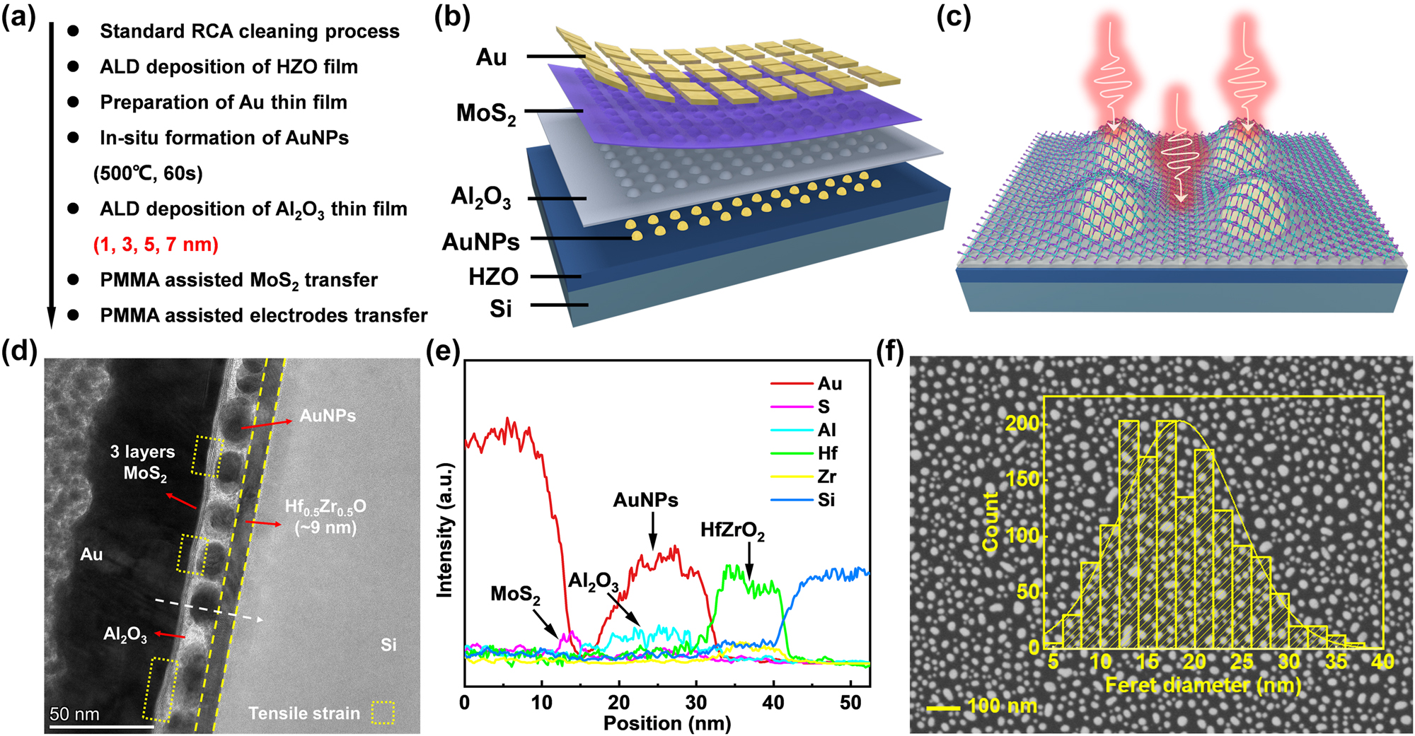
Fabrication process and microstructural characterization of the NC-LSPR phototransistor: (a) the preparation process; (b) schematic diagram and (c) atomic structure of the NC-LSPR-coupled phototransistor; (d) high-resolution TEM image of cross-section of the AuNPs/Al2O3/MoS2 stack; (e) line-scanning element distribution along the white dash line in (d) for Au, Mo, S, Al, Hf, Zr and Si; (f) scanning electron microscopy (SEM) image of the AuNPs, showcasing a normal distribution of diameter primarily concentrated at 15–20 nm.
The NC-LSPR coupled gate-stack structure is shown in Figure 1(c). This structure combines the NC effect from the HZO film [16], [17], [18] with the LSPR effect from the AuNPs [21], [22] to enhance the photocurrent (I ph). The Al2O3 layer, located between the AuNPs and MoS2, serves as both an interface passivation layer (IPL) and a CML to improve interfacial quality and enhance the NC effect. Additionally, the ALD-deposited Al2O3 thin film maintains the tensile strain across the MoS2 film induced by the AuNPs, thereby stretching the lattice of MoS2 and reducing its bandgap [14].
Figure 1(d) presents a high-resolution transmission electron microscopy (HRTEM) image of the NC-LSPR structure. A distinct layered structure of Si/HZO/AuNPs/Al2O3/MoS2/Au and diffusion-free clean interfaces are clearly visible. The HZO layer, with its well-defined crystalline structure, is 9 nm thick. The AuNPs exhibit a dispersed and rounded granularity, and the three-layered MoS2 has a thickness of ∼2.1 nm. Notably, the amorphous Al2O3 layer is visible between the MoS2 and AuNPs, and the in-plane tensile strain of MoS2 due to the AuNPs is highlighted within the yellow dashed box in Figure 1(d). Figure 1(e) shows the line scanning elemental distributions for Au, Mo, S, Hf, Zr and Si along the white dashed line in Figure 1(d), revealing distinct elemental peaks corresponding to MoS2, Al2O3, AuNPs and HZO. Additionally, Figure 1(f) provides a scanning electron microscopy (SEM) image of the AuNPs array. The nanoparticle diameter has been analyzed using ImageJ, and the resulting normal distribution curve indicates that the diameter of the AuNPs is predominantly in a range of 15–20 nm.
To investigate the influence of T AlO on the LSPR effect as well as the strain effect across the MoS2 film in the AuNPs/Al2O3/MoS2 structure, COMSOL simulations were performed for the stacked structure with different T AlO values of 1 nm (a1), 3 nm (a2), 5 nm (a3) and 7 nm (a4). In the COMSOL simulation, the lateral period is set to 65 nm, with a perfect matching layer placed in the vertical direction at a distance of 760 nm from the device with a width of 380 nm. The nanoparticle diameter is 17 nm, and the mesh size is set to be 0.2 nm in both lateral and vertical directions. Also, a curved A2O3 layer covers the AuNPs to align the model with the experimental geometry [23] (the simulation result of the source-drain area with Au electrode is plotted in Figure S1 in Supporting Information). The electric-field distribution obtained from the simulation is shown in Figure 2(a). It is evident that the electric field corresponding to the LSPR effect decreases gradually with increasing T AlO. Figure 2(b) and (c) display the measured and simulated light absorption spectra from pure MoS2, AuNPs/MoS2 and AuNPs/Al2O3/MoS2 with different T AlO, respectively. In Figure 2(b), three exciton peaks at A (653 nm), B (605 nm) and C (430 nm) correspond to pure MoS2 [24], and the exciton peak at 550 nm corresponds to the LSPR effect induced by AuNPs [22], [25]. These four exciton peaks are also observed in Figure 2(c). Both experimental data and simulation results exhibit the same pattern: compared to pure MoS2, the AuNPs/MoS2 structures show distinct LSPR peaks, which decreases gradually with increasing T AlO.
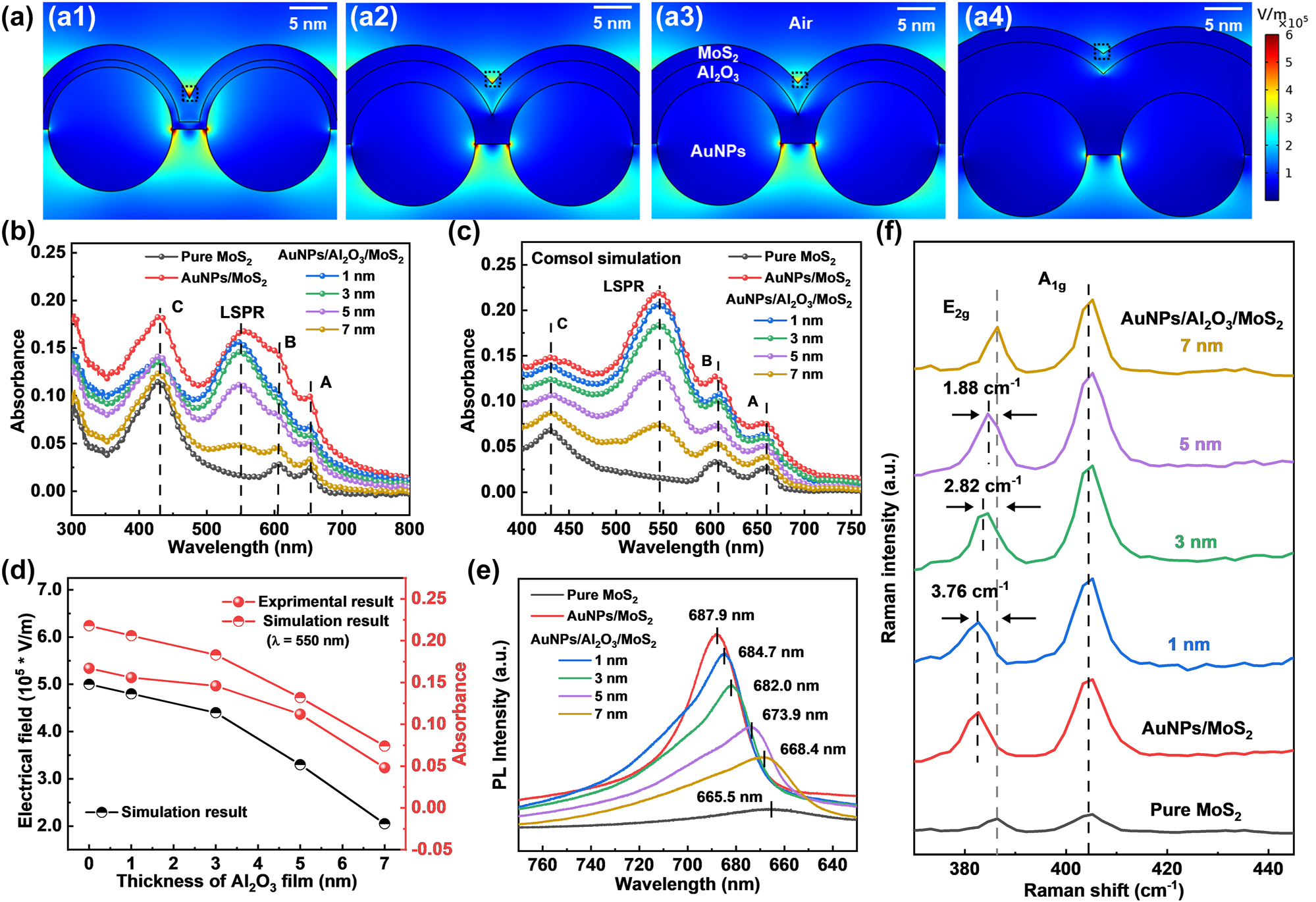
Characterization of the LSPR effect and stress-induced effects in AuNPs/Al2O3/MoS2 with different Al2O3 thickness: (a) electrical-field distributions of LSPR effect and (b) light absorption spectra simulated using COMSOL; (c) measured result of the light absorption spectra; (d) the electric field strength in the black dashed box in (a) and the LSPR peaks in the optical absorption spectra of (b) and (c) (λ = 550 nm); (e) PL and (f) Raman spectra corresponding to the tensile strain of MoS2 induced by AuNPs and the dielectric screening effect of Al2O3 layer.
For comparison, the electric field strength in the black dashed box in Figure 2(a) and the LSPR peaks in Figure 2(b) and (c) are extracted as Figure 2(d). It can be seen that when T AlO is less than 3 nm, the electric-field strength decreases at a rate of ∼2.0 × 10⁴ Vm−1/nm, and when T AlO exceeds 3 nm, the electric-field strength decreases at an increased rate of ∼5.9 × 10⁴ Vm−1/nm. Similarly, the LSPR peaks obtained from COMSOL simulations and experiments exhibit a slow decreasing trend for T AlO’s of ≤3 nm (measured results: 0.007/nm) and a rapid decreasing trend for T AlO’s of >3 nm (measured results: 0.0245/nm). These results suggest that the NDC-LSPR effect in the AuNPs/Al2O3/MoS2 stack is less affected for thin T AlO’s (≤3 nm) and rapidly weakened for relatively thick T AlO’s (>3 nm).
Furthermore, the tensile strain of MoS2 induced by AuNPs can be characterized by Raman and PL spectra. The PL spectra are given in Figure 2(e), where the solid black line represents a distinct peak from pure MoS2 at 665.5 nm. The corresponding peak of the AuNPs/MoS2 stack undergoes a significant redshift of 22.4 nm [26], [27], whose intensity gradually weakens with increasing T AlO, specifically a redshift of 16.5 nm at 3 nm and 2.9 nm at 7 nm. In the Raman spectra shown in Figure 2(f), two main peaks corresponding to the A1g (404.3 cm−1) and E2g modes (386.5 cm−1) can be observed in pure MoS2 [28], in which the E2g mode is significantly redshifted (towards lower wavenumbers) due to the addition of AuNPs [14], [27], and the redshift decreases for the AuNPs/Al2O3/MoS2 stack with increasing T AlO. These redshifts in Raman and PL spectra are originated from the bandgap reduction due to the strain effect, which enhances the long-wave absorption capability of MoS2 [15], [26], [27]. However, the nanoscale particle morphology of AuNPs is gradually covered by the Al2O3 layer with increasing T AlO (see Figure S2 in Supporting Information), leading to a significant reduction of the tensile strain across the MoS2 film. In addition, it is worth to point out that the blueshift of PL peak [29], [30] with the increasing T AlO is not only due to the weakening of the strain on MoS2, but also attributed to the dielectric screening effect of Al2O3 layer on the Coulomb interactions either between electrons and holes or between different electrons in MoS2 [29], [30], [31].
To illustrate the variation trend of the electrical properties of devices with Al2O3 thickness and optimize capacitance-matched thickness of Al2O3, the electrical performances of pure MoS2, AuNPs/MoS2 and different T AlO’s AuNPs/Al2O3/MoS2 phototransistors are measured and given in Figure 3. The polarization and current versus electric field (P–E and I–E) loops of the TiN/(HZO/AuNPs)/Au capacitor at a frequency of 1 kHz are shown in Figure 3(a). The P–E loop exhibits good ferroelectric polarization with a fixed residual polarization (P r) of 13.1 μC/cm2, and a pronounced polarization reversal current [19] is observed at a fixed coercive field (E c) of 1.1 MV/cm. Figure 3(b) shows the transfer curves of the phototransistors in the dark state at a drain-source voltage (V ds) of 0.1 V. The on-state current (I on), off-state current (I off), and current switching ratio (I on/I off) extracted from the transfer curves are plotted in Figure 3(c), where T AlO = 0 nm corresponds to the transistor with a gate stack of p+-Si/(HZO/AuNPs)/MoS2/Au, and “Pure MoS2” represents the transistor with a gate stack of p+-Si/HZO/MoS2/Au. Compared to the pure MoS2 device, the electrical performance of the AuNPs/MoS2 device is significantly degraded, mainly due to the formation of leakage paths created by the AuNPs. Fortunately, electrical properties of the AuNPs/Al2O3/MoS2 device with T AlO in a range of 0–3 nm are greatly improved due to the isolation of those leakage paths by the Al2O3 interlayer [15] and the enhanced NC effect resulting from the capacitance-matched ferroelectric HZO layer [17], [18]. For the device with T AlO = 3 nm, the I on, I off and I on/I off ratio are extracted to be 2.8 × 10⁻⁷ A, 1.0 × 10⁻¹² A and 2.8 × 10⁵, respectively. After T AlO exceeds 3 nm, I on decreases and I off rises slightly, resulting in a decreasing trend in I on/I off. At T AlO = 7 nm, the I on, I off and I on/I off are 2.1 × 10⁻⁷ A, 2.2 × 10⁻¹² A, and 9.9 × 10⁴, respectively. This reduction in I on/I off is attributed to the capacitive mismatch between the Al2O3 and HZO layers [32]. The subthreshold swing (SS) of transistors extracted from Figure 3(b) is plotted in Figure 3(d). The SS increases significantly with the addition of AuNPs but decreases after the insertion of the Al2O3 interlayer. At T AlO = 3 nm, the SS remains below 60 mV/dec from 10−12 to 10−10 A, with a lowest SS of 25.76 mV/dec. For T AlO’s of >3 nm, the SS gradually increases, and at T AlO = 7 nm, the SS is below 60 mV/dec only in a small range of drain current (I d). Further, the hysteresis of the transfer curves and the minimum SS are demonstrated in Figure 3(e). Consistent with SS variation, hysteresis increases sharply with the addition of AuNPs and achieves a minimum (348 ± 85 mV) at a T AlO of 3 nm after the insertion of the Al2O3 interlayer, and then increases again when T AlO exceeds 3 nm. The degradation of I on/I off, SS and hysteresis after T AlO exceeds 3 nm can be explained by the C–V results in Figure 3(f). The C–V curves were measured on the Si/HZO/(AuNPs or AuNPs/Al2O3)/Au capacitor at a frequency of 5 kHz. The total capacitance C −1 = C Fe −1 + C MOS −1 (C Fe is the ferroelectric capacitance of the HZO layer, C MOS is the MOS capacitance), and the C–V curves display a sharp peak due to the NC effect of the HZO layer [33]. It can be seen that the capacitance peak is highest at a T AlO of 3 nm, indicating that the NC-LSPR structure with a 3-nm Al2O3 interlayer can obtain the best capacitance matching effect [32], [34].
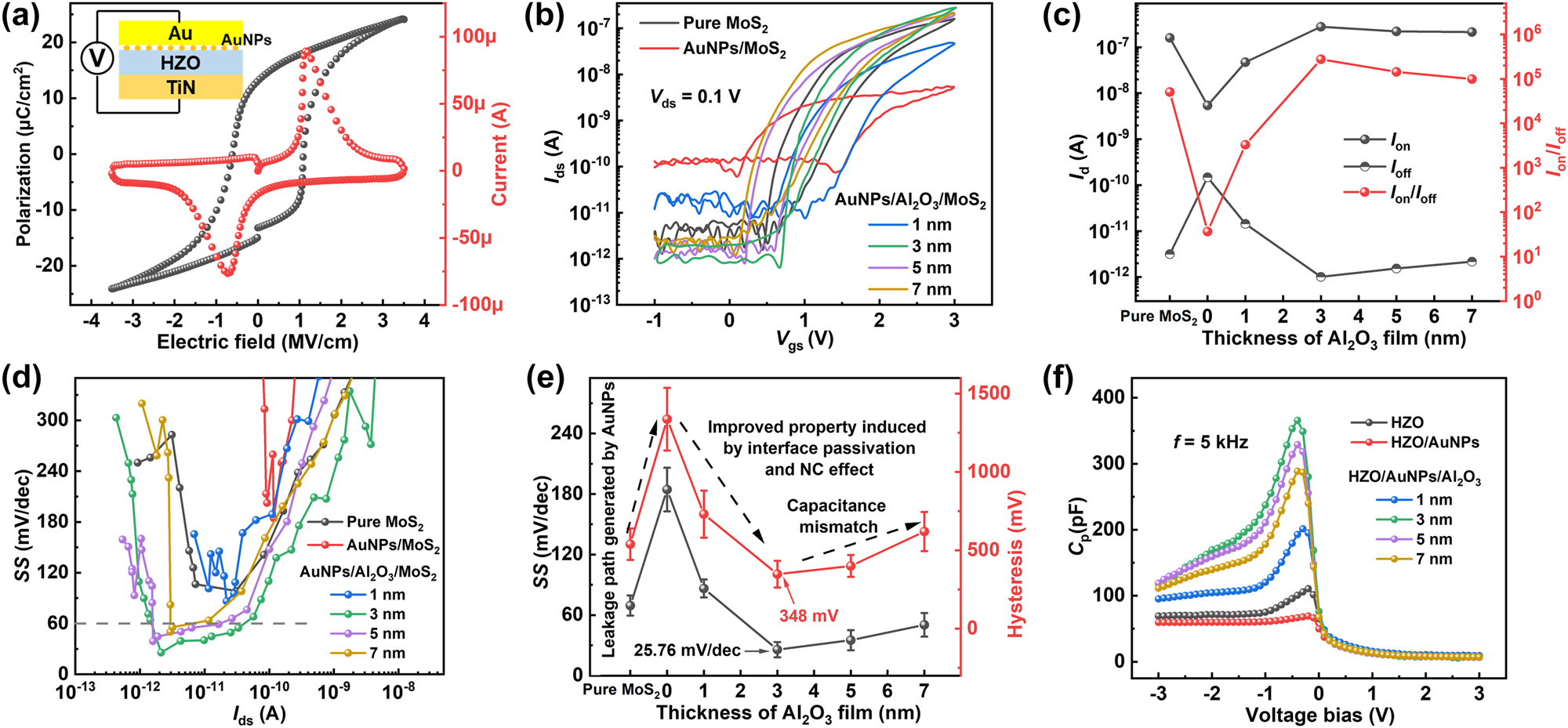
Electrical properties of pure MoS2, AuNPs/MoS2 and different T AlO’s AuNPs/Al2O3/MoS2 phototransistors: (a) P–E loop and I–E loop measured on TiN/HZO/AuNPs/Au capacitor at a frequency of 1 kHz; (b) transfer curves at a V ds of 0.1 V in the dark state; (c) variation of I on, I off and I on/I off ratio extracted from (b) with Al2O3 thickness, where T AlO = 0 nm corresponds to the transistor with a gate stack of p+-Si/HZO/AuNPs/MoS2/Au, and “Pure MoS2” represents the transistor with a gate stack of p+-Si/HZO/MoS2/Au; (d) SS versus I d curves of the phototransistors; (e) the hysteresis and minimum SS for different devices with different T AlO’s; (f) C–V curves measured on the p-Si/HZO/(AuNPs or AuNPs/Al2O3)/Au capacitor at a frequency of 5 kHz.
To investigate how the change in T AlO affects the optical performance of the phototransistor, the optical performance of the NC-LSPR-coupled phototransistor is measured using the circuit connection shown in Figure 4(a) under different light intensities (P). The laser was vertically incident and the light intensity reaching the sample surface was adjusted using attenuators. The transfer curves at a V ds of 0.1 V and the output curves at a gate-source voltage (V gs) of 0.7 V of the phototransistor with a 3-nm T AlO are measured in the dark state and under 528-nm illumination, as shown in Figure 4(b) and (c) respectively. The photogenerated current I ph (I ph = I light − I dark), responsivity R (R = I ph/P i ) and detectivity D ∗ (D ∗ = RA 1/2 (2eI dark)−1/2) are extracted from Figure 4(c) and plotted in Figure 4(e), where I light and I dark is the I d under illumination and in dark state, respectively. The incident light power P i = AP, A is the area of the MoS2 channel region (240 μm2). It can be observed that the R and D ∗ of the device with a T AlO of 3 nm are 140.1 A/W and 3.83 × 10¹⁴ Jones at P = 2.36 μW/cm2, respectively. The R and D ∗ decrease progressively with increasing P, which is consistent with the previous work [15]. Therefore, in order to better compare the optical performance of the devices, the I ph values of these phototransistors at P = 2.36 μW/cm2 and V ds = 0.4 V are shown in Figure 4(d), from which the R and D ∗ are calculated as a function of T AlO, as shown in Figure 4(f). Compared with pure MoS2, the smaller photocurrent of AuNPs/MoS2 should be attributed to the reduced mobility by surface roughness scattering [35], [36] due to a poor interfacial quality between AuNPs and MoS2 and the formation of source-drain leakage channels. Then, as T AlO increases, the I ph, R and D ∗ exhibit an increasing and then decreasing trend, in which the device with T AlO = 3 nm achieves the best photodetection characteristics of R = 140.1 A/W and D ∗ = 3.83 × 10¹⁴ Jones. Additionally, I ph of the device with T AlO = 3 nm at different polarization angles is provided in Figure S3 in the Supporting Information.
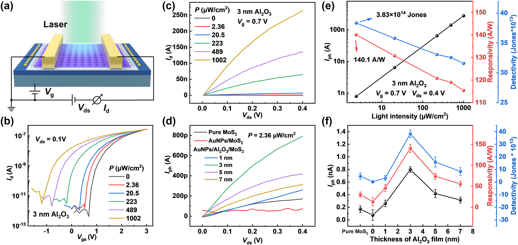
Optical performance of the phototransistor: (a) circuit schematic for the optical-performance measurement; (b) transfer curves and (c) output curves in the dark state and under 528-nm illumination for the device with a T AlO of 3 nm; (d) I ph versus V ds curves of all phototransistors at P = 2.36 μW/cm2; (e) I ph, R and D * under different light intensities extracted from (c), where the highest R and D * are obtained at P = 2.36 μW/cm2; (f) I ph, R and D * for different phototransistors at V ds = 0.4 V and P = 2.36 μW/cm2.
For those phototransistors with T
AlO < 3 nm, despite a strong LSPR effect, the poor electrical properties result in a smaller photogenerated current due to interface issues caused by AuNPs and non-optimal capacitance matching. Since
To figure out the influence of the T AlO on tensile strain across the MoS2, the photocurrent versus time curves of all phototransistors under 528 nm or 740 nm illumination are presented in Figure 5(a) and (b), respectively (with one light on/off cycle for each device). A significant photocurrent can be observed for all the devices as the light switches at 528 nm illumination, where the photocurrent for the device with T AlO = 3 nm is ∼811 nA. Nevertheless, under 740 nm illumination, the photocurrent of the pure MoS2 device is almost indistinguishable, and the photocurrent of the AuNPs/MoS2 device is notably noisy. Following the insertion of Al2O3 interlayer, the photocurrent gradually increases while the noise decreases, and reaches a maximum value at T AlO = 3 nm (∼216 pA). When T AlO > 3 nm, the photocurrent starts to reduce and at T AlO = 7 nm, the photocurrent exhibits significant noise again, primarily due to the attenuation of the strain effect on MoS2 with increasing T AlO, which aligns with the conclusions drawn from Figure 2(e) and (f). The normal distributions as well as box plots of the R and D ∗ calculated from the photocurrents of 30 devices are plotted in Figure 5(c). Under 528 nm and 740 nm illumination, the extracted average D ∗ values were 3.823 × 10¹⁴ Jones and 1.097 × 10¹⁴ Jones, respectively, indicating that the devices have a wide spectral response range, ultrahigh detectivity and excellent consistency.

The photocurrent versus time curves of all phototransistors under (a) 528 nm and (b) 740 nm illumination; (c) the normal distributions and box plots of the R and D * calculated from the photocurrents of 30 devices; (d) the detectivity at different detection wavelengths for MoS2 phototransistors optimized by different methods.
Figure 5(d) compares the detectivities at different detection wavelengths for MoS2 phototransistors optimized by different methods [37], [38], [39], [40], [41], [42], [43] (The specific data for detectivity and wavelength from the references in Figure 5(d) can be seen in Table S1 in Supporting Information). The LSPR-enhanced devices and CTA devices can broaden the detection range, but their detectivities remained below 1012 Jones due to increased dark current. Conversely, the NC effect-enhanced devices achieved a detectivity above 1014 Jones, far exceeding conventional MoS2 transistors. Innovatively, this work combines the high detectivity from the NC effect with the enhanced detection range from the LSPR effect and optimize the Al2O3 thickness by considering its influence on the LSPR effect, the strain effect, the NC capacitance matching effect and the modulation of the optoelectronic properties. Ultimately, a high detectivity of more than 1014 Jones and excellent uniformity were achieved for the NC-LSPR coupling structure of HZO/AuNPs/3 nm Al2O3/MoS2 under 740 nm illumination. This provides a theoretical basis and an experimental support for further applications of the NC-LSPR coupling structures and paves a way for the preparation of 2D high-performance photodetector array.
3 Conclusions
In summary, the influences of the thicknesses of Al2O3 interlayer on the LSPR effect, the tensile stress across the MoS2, the NC effect and optoelectronic properties of the NC-LSPR coupled phototransistors with a gate stack of HZO/AuNPs/Al2O3/MoS2 have been investigated. It has been found that at T AlO < 3 nm, the strong LSPR and stress effects can be maintained, and at T AlO of 3 nm, the NC-LSPR coupled structure could obtain the best capacitance matching effect as well as the optimized optoelectrical characteristics, i.e. a SS of 25.76 mV/dec and a detectivity of 3.823 × 10¹⁴/1.097 × 1014 Jones under 528 nm/740 nm illumination with a good uniformity. The involved mechanisms lie in a good capacitance matching and effective interface passivation provided by optimizing Al2O3 thickness in the gate stack of HZO/AuNPs/Al2O3/MoS2 to enhance the NC-LSPR coupling effect, and results in an extremely low SS, enhanced optical absorption due to the obvious LSPR effect and an extended detection range owing to the strain in the MoS2. This work provides an in-depth insight on the variation of optoelectrical properties of the NC-LSPR coupled devices with increasing T AlO, and broadens the way for preparing high-performance 2D photodetector array.
4 Methods
4.1 PMMA assisted transfer process
The CVD-MoS2 was grown on Si/SiO2 substrate (purchased from Sixcarbon Technology Shenzhen) and then covered by PMMA at a speed of 3,000 rpm for 30 s and baking at 150 °C for 5 min. The MoS2/PMMA was released onto the target surface by wet transfer with HF solution, and then annealed at 150 °C for 4 h, followed by soaking in acetone solution for 12 h to remove the PMMA. The 100-nm Au electrodes (prepared on pre-patterned Si/SiO2 substrates) were also transferred by the same process.
4.2 Measurements of photoelectric properties
The transfer, output and I ph versus time curves of transistor under dark state and light illumination are measured by Keysight B1500A semiconductor parameter analyzer at room temperature. The 528-nm and 740-nm lasers are chosen as the light source for photoresponse measurement in light tight and electrically shielded ambient.
Funding source: National Natural Science Foundation of China
Award Identifier / Grant number: 61974048
Award Identifier / Grant number: 92264107
-
Research funding: This work was supported by the National Natural Science Foundation of China (Grant No. 92264107, 61974048).
-
Author contributions: All authors have accepted responsibility for the entire content of this manuscript and approved its submission.
-
Conflict of interest: Authors state no conflicts of interest.
-
Data availability: The datasets generated during and analyzed during the current study are available from the corresponding author on reasonable request.
References
[1] K. S. Novoselov, A. Mishchenko, A. Carvalho, and A. H. Castro Neto, “2D materials and van der Waals heterostructures,” Science, vol. 353, no. 6298, p. 9439, 2016. https://doi.org/10.1126/science.aac9439.Suche in Google Scholar PubMed
[2] W. Su, et al.., “Interlayer transition induced infrared response in ReS2/2D perovskite van der Waals heterostructure photodetector,” Nano Lett., vol. 22, no. 24, 2022, Art. no. 10192. https://doi.org/10.1021/acs.nanolett.2c04328.Suche in Google Scholar PubMed
[3] F. Bonaccorso, Z. Sun, T. Hasan, and A. C. Ferrari, “Graphene photonics and optoelectronics,” Nat. Photonics, vol. 4, no. 9, p. 611, 2010. https://doi.org/10.1038/nphoton.2010.186.Suche in Google Scholar
[4] Y. Xie, et al.., “Room‐temperature ultrabroadband photodetection with MoS2 by electronic‐structure engineering strategy,” Adv. Mater., vol. 30, no. 50, 2018, Art. no. 1804858. https://doi.org/10.1002/adma.201804858.Suche in Google Scholar PubMed
[5] M. M. Furchi, D. K. Polyushkin, A. Pospischil, and T. Mueller, “Mechanisms of photoconductivity in atomically thin MoS2,” Nano Lett., vol. 14, no. 11, p. 6165, 2014. https://doi.org/10.1021/nl502339q.Suche in Google Scholar PubMed
[6] H. J. Conley, B. Wang, J. I. Ziegler, R. F. Haglund, S. T. Pantelides, and K. I. Bolotin, “Bandgap engineering of strained monolayer and bilayer MoS2,” Nano Lett., vol. 13, no. 8, p. 3626, 2013. https://doi.org/10.1021/nl4014748.Suche in Google Scholar PubMed
[7] O. Lopez-Sanchez, D. Lembke, M. Kayci, A. Radenovic, and A. Kis, “Ultrasensitive photodetectors based on monolayer MoS2,” Nat. Nanotechnol., vol. 8, no. 7, p. 497, 2013. https://doi.org/10.1038/nnano.2013.100.Suche in Google Scholar PubMed
[8] M. Bernardi, M. Palummo, and J. C. Grossman, “Extraordinary sunlight absorption and one nanometer thick photovoltaics using two-dimensional monolayer materials,” Nano Lett., vol. 13, no. 8, p. 3664, 2013. https://doi.org/10.1021/nl401544y.Suche in Google Scholar PubMed
[9] Z. Xu, et al.., “Monolayer MoS2/GaAs heterostructure self-driven photodetector with extremely high detectivity,” Nano Energy, vol. 23, p. 89, 2016. https://doi.org/10.1016/j.nanoen.2016.03.011.Suche in Google Scholar
[10] D.-H. Kang, et al.., “An ultrahigh‐performance photodetector based on a perovskite–transition‐metal‐dichalcogenide hybrid structure,” Adv. Mater., vol. 28, no. 35, p. 7799, 2016. https://doi.org/10.1002/adma.201600992.Suche in Google Scholar PubMed
[11] D. Kufer, I. Nikitskiy, T. Lasanta, G. Navickaite, F. H. L. Koppens, and G. Konstantatos, “Hybrid 2D-0D MoS2 -PbS quantum dot photodetectors,” Adv. Mater., vol. 27, no. 1, p. 176, 2015. https://doi.org/10.1002/adma.201402471.Suche in Google Scholar PubMed
[12] S. H. Yu, et al.., “Dye-sensitized MoS2 photodetector with enhanced spectral photoresponse,” ACS Nano, vol. 8, no. 8, p. 8285, 2014. https://doi.org/10.1021/nn502715h.Suche in Google Scholar PubMed
[13] J. Li, et al.., “Enhancement of the photoresponse of monolayer MoS2 photodetectors induced by a nanoparticle grating,” ACS Appl. Mater. Interfaces, vol. 12, no. 7, p. 8429, 2020. https://doi.org/10.1021/acsami.9b20506.Suche in Google Scholar PubMed
[14] D. Lu, et al.., “Strain-Plasmonic coupled broadband photodetector based on monolayer MoS2,” Small, vol. 18, no. 14, 2022, Art. no. 2107104. https://doi.org/10.1002/smll.202107104.Suche in Google Scholar PubMed
[15] W. Jiang, Y. Deng, S. Rui, J. Xu, and L. Liu, “High-detectivity and broadband MoS2 phototransistor array by coupling negative capacitance and local surface plasmon resonance effects,” ACS Photonics, vol. 11, no. 6, p. 2308, 2024. https://doi.org/10.1021/acsphotonics.4c00183.Suche in Google Scholar
[16] V. Gaddam, D. Das, T. Jung, and S. Jeon, “Ferroelectricity enhancement in Hf0.5Zr0.5O2-based tri-layer capacitors at low-temperature (350°C) annealing process,” IEEE Electron Device Lett., vol. 42, no. 6, pp. 812–815, 2021. https://doi.org/10.1109/led.2021.3075082.Suche in Google Scholar
[17] L. Tu, et al.., “Ultrasensitive negative capacitance phototransistors,” Nat. Commun., vol. 11, no. 1, p. 101, 2020. https://doi.org/10.1038/s41467-019-13769-z.Suche in Google Scholar PubMed PubMed Central
[18] X. Guo, et al.., “Optimization of subthreshold swing and hysteresis in Hf0.5Zr0.5O2-based MoS2 negative capacitance field-effect transistors by modulating capacitance matching,” ACS Appl. Mater. Interfaces, vol. 15, no. 26, 2023, Art. no. 31617. https://doi.org/10.1021/acsami.3c04595.Suche in Google Scholar PubMed
[19] W. Jiang, L. Liu, and J. Xu, “Improved detectivity and response speed of MoS2 phototransistors based on the negative-capacitance effect and defect engineering,” Opt. Express, vol. 30, no. 26, 2022, Art. no. 46070. https://doi.org/10.1364/oe.475102.Suche in Google Scholar PubMed
[20] T. S. Böscke, J. Müller, D. Bräuhaus, U. Schröder, and U. Böttger, “Ferroelectricity in hafnium oxide thin films,” Appl. Phys. Lett., vol. 99, no. 10, 2011, Art. no. 102903. https://doi.org/10.1063/1.3634052.Suche in Google Scholar
[21] C. Wang, et al.., “Direct plasmon-accelerated electrochemical reaction on gold nanoparticles,” ACS Nano, vol. 11, no. 6, pp. 5897–5905, 2017. https://doi.org/10.1021/acsnano.7b01637.Suche in Google Scholar PubMed
[22] Y. Li, et al.., “Au@MoS2 core–shell heterostructures with strong light–matter interactions,” Nano Lett., vol. 16, no. 12, p. 7696, 2016. https://doi.org/10.1021/acs.nanolett.6b03764.Suche in Google Scholar PubMed
[23] W. Chen, et al.., “Probing the limits of plasmonic enhancement using a two-dimensional atomic crystal probe,” Light: Sci. Appl., vol. 7, no. 1, p. 56, 2018. https://doi.org/10.1038/s41377-018-0056-3.Suche in Google Scholar PubMed PubMed Central
[24] S. Zhang, et al.., “Direct observation of degenerate two-photon absorption and its saturation in WS2 and MoS2 monolayer and few-layer films,” ACS Nano, vol. 9, no. 7, p. 7142, 2015. https://doi.org/10.1021/acsnano.5b03480.Suche in Google Scholar PubMed
[25] Y. Liu, et al.., “Plasmon resonance enhanced multicolour photodetection by graphene,” Nat. Commun., vol. 2, no. 1, p. 579, 2011. https://doi.org/10.1038/ncomms1589.Suche in Google Scholar PubMed PubMed Central
[26] A. Castellanos-Gomez, et al.., “Local strain engineering in atomically thin MoS2,” Nano Lett., vol. 13, no. 11, p. 5361, 2013. https://doi.org/10.1021/nl402875m.Suche in Google Scholar PubMed
[27] B. Liu, et al.., “Strain-engineered van der Waals interfaces of mixed-dimensional heterostructure arrays,” ACS Nano, vol. 13, no. 8, p. 9057, 2019. https://doi.org/10.1021/acsnano.9b03239.Suche in Google Scholar PubMed
[28] H. Li, et al.., “Optoelectronic crystal of artificial atoms in strain-textured molybdenum disulphide,” Nat. Commun., vol. 6, no. 1, p. 7381, 2015. https://doi.org/10.1038/ncomms8381.Suche in Google Scholar PubMed PubMed Central
[29] Y. Lin, et al.., “Dielectric screening of excitons and trions in single-layer MoS2,” Nano Lett., vol. 14, no. 10, pp. 5569–5576, 2014. https://doi.org/10.1021/nl501988y.Suche in Google Scholar PubMed
[30] D. V. Tuan and H. Dery, “Effects of dynamical dielectric screening on the excitonic spectrum of monolayer semiconductors,” Phys. Rev. B, vol. 110, no. 12, 2024, Art. no. 125301. https://doi.org/10.1103/physrevb.110.125301.Suche in Google Scholar
[31] F. Prins, A. J. Goodman, and W. A. Tisdale, “Reduced dielectric screening and enhanced energy transfer in single-and few-layer MoS2,” Nano Lett., vol. 14, no. 11, pp. 6087–6091, 2014. https://doi.org/10.1021/nl5019386.Suche in Google Scholar PubMed
[32] J. Wang, L. Liu, Y. Xia, and J. Xu, “Improved tradeoff between subthreshold swing and hysteresis for MoS2 negative-capacitance FETs by optimizing gate-stack of Hf1−xZrxO2/Al2O3,” IEEE Trans. Electron Devices, vol. 68, no. 12, p. 6546, 2021. https://doi.org/10.1109/ted.2021.3118330.Suche in Google Scholar
[33] D. Jimenez, E. Miranda, and A. Godoy, “Analytic model for the surface potential and drain current in negative capacitance field-effect transistors,” IEEE Trans. Electron Devices, vol. 57, no. 10, p. 2405, 2010. https://doi.org/10.1109/ted.2010.2062188.Suche in Google Scholar
[34] A. I. Khan, U. Radhakrishna, S. Salahuddin, and D. Antoniadis, “Work function engineering for performance improvement in leaky negative capacitance FETs,” IEEE Electron Device Lett., vol. 38, no. 9, p. 1335, 2017. https://doi.org/10.1109/led.2017.2733382.Suche in Google Scholar
[35] K. Uchida, H. Watanabe, A. Kinoshita, and J. Koga, “Experimental study on carrier transport mechanism in ultrathin-body SOI nand p-MOSFETs with SOI thickness less than 5 nm,” in Digest. International Electron Devices Meeting, San Francisco, 2002, pp. 47–50.10.1109/IEDM.2002.1175776Suche in Google Scholar
[36] Z. Yu, et al.., “Analyzing the carrier mobility in transition‐metal dichalcogenide MoS2 field‐effect transistors,” Adv. Funct. Mater., vol. 27, no. 19, 2017, Art. no. 1604093. https://doi.org/10.1002/adfm.201604093.Suche in Google Scholar
[37] F. Gong, et al.., “High-sensitivity floating-gate phototransistors based on WS2 and MoS2,” Adv. Funct. Mater., vol. 26, no. 33, p. 6084, 2016. https://doi.org/10.1002/adfm.201601346.Suche in Google Scholar
[38] S. Lee, J. Park, Y. Yun, J. Lee, and J. Heo, “Enhanced photoresponsivity of multilayer MoS2 phototransistor using localized Au Schottky junction formed by spherical-lens photolithography,” Adv. Mater. Interfaces, vol. 6, no. 8, 2019, Art. no. 1900053. https://doi.org/10.1002/admi.201900053.Suche in Google Scholar
[39] B. Rahmati, I. Hajzadeh, M. Taheri, R. Karimzadeh, S. Mohajerzadeh, and S. M. Mohseni, “Plasmonic improvement of photoresponse in vertical-MoS2 nanostructure photodetector by Au nanoparticles,” Appl. Surf. Sci., vol. 490, no. 1, p. 165, 2019. https://doi.org/10.1016/j.apsusc.2019.06.058.Suche in Google Scholar
[40] D.-S. Tsai, et al.., “Few-layer MoS2 with high broadband photogain and fast optical switching for use in harsh environments,” ACS Nano, vol. 7, no. 5, p. 3905, 2013. https://doi.org/10.1021/nn305301b.Suche in Google Scholar PubMed
[41] Y. Lee, et al.., “Trap-induced photoresponse of solution-synthesized MoS2,” Nanoscale, vol. 8, no. 17, p. 9193, 2016. https://doi.org/10.1039/c6nr00654j.Suche in Google Scholar PubMed
[42] W. Choi, et al.., “High-detectivity multilayer MoS2 phototransistors with spectral response from ultraviolet to infrared,” Adv. Mater., vol. 24, no. 43, p. 5832, 2012. https://doi.org/10.1002/adma.201201909.Suche in Google Scholar PubMed
[43] D. Kufer and G. Konstantatos, “Highly sensitive, encapsulated MoS2 photodetector with gate controllable gain and speed,” Nano Lett., vol. 15, no. 11, p. 7307, 2015. https://doi.org/10.1021/acs.nanolett.5b02559.Suche in Google Scholar PubMed
Supplementary Material
This article contains supplementary material (https://doi.org/10.1515/nanoph-2024-0371).
© 2024 the author(s), published by De Gruyter, Berlin/Boston
This work is licensed under the Creative Commons Attribution 4.0 International License.
Artikel in diesem Heft
- Frontmatter
- Review
- Plasmon-driven molecular scission
- Research Articles
- Ultra-compact thin-film-lithium-niobate photonic chip for dispersion compensation
- Optimization of NC-LSPR coupled MoS2 phototransistors for high-performance broad-spectrum detection
- Impact of temperature on the brightening of neutral and charged dark excitons in WSe2 monolayer
- Designing rotational motion of charge densities on plasmonic nanostructures excited by circularly polarized light
- Twist-tunable in-plane anisotropic polaritonic crystals
- An overview on plasmon-enhanced photoluminescence via metallic nanoantennas
- Unique features of plasmonic absorption in ultrafine metal nanoparticles: unity and rivalry of volumetric compression and spill-out effect
- Constant-force photonic projectile for long-distance targeting delivery
- Emission dynamics and spectrum of a nanoshell-based plasmonic nanolaser spaser
- Degeneracy mediated thermal emission from nanoscale optical resonators with high-order symmetry
- Erratum
- Corrigendum to: modeling with graded interfaces: tool for understanding and designing record-high power and efficiency mid-infrared quantum cascade lasers