Ultra-compact thin-film-lithium-niobate photonic chip for dispersion compensation
-
Shujun Liu
 und
Daoxin Dai
und
Daoxin Dai


Abstract
Thin-film-lithium-niobate (TFLN) photonics has attracted intensive attention and become very popular in recent years. Here, an ultra-compact TFLN on-chip dispersion compensator is proposed and realized to provide a promising solution for dispersion control. The proposed dispersion compensator is composed of chirped multimode waveguide gratings (CMWGs) arranged in zigzag-cascade, enabling high footprint compactness and scalability. Particularly, these CMWGs are circulator-free and very convenient for cascading, owing to the TE0–TE1 mode conversion and the assistance of the TE0–TE1 mode (de)multiplexer. The present configuration with CMWGs in zigzag-cascade also overcomes the drawback of being unable to use waveguide spirals for large-range time delay and dispersion control due to the TFLN’s anisotropy. In addition, positive/negative dispersion control is realized by appropriately choosing the input port of the CMWGs. In the experiment, 2-mm-long CMWGs are used to provide a dispersion value of about +1.5 ps/nm and −1.2 ps/nm over a 21-nm-wide bandwidth, and there are up to 32 CMWGs in cascade demonstrated experimentally, showing a maximal dispersion of 49.2 ps/nm and −39.3 ps/nm. The corresponding average propagation loss is as low as 0.47 dB/cm, and the fabricated chip with 32 CMWGs in zigzag-cascade has a footprint as compact as 0.16 × 4.65 mm2. Finally, the present on-chip dispersion compensator is used successfully to compensate for the dispersion originating from a 5-km-long singlemode fiber (SMF) and high-quality eye-diagrams are achieved for the recovered 40 Gbps OOK signals, showing great potential for optical systems such as high-speed interconnects in datacenters.
1 Introduction
Chromatic dispersion management is a crucial problem in optical systems, which is caused by the different propagation speeds of different wavelengths in optical paths. Generally, dispersion is often realized by manipulating the group velocity. Dispersion controllers are widely utilized across a spectrum of optical systems, including optical communication, microwave photonics, and nonlinear optics. They play a crucial role in managing precise time delays and pulse profiles with accuracy [1], [2], [3], [4]. As a key device in system-level applications, dispersion controllers are required to be realized flexibly with various material platforms. In recent years, TFLN photonics has exhibited promising prospects because of its unique excellence, like high linear electro-optic (EO) coefficient, low propagation loss, and high stability [5]. In the past years, high-quality dry-etching technology has been developed for making low-loss TFLN photonic waveguides [6] and many high-performance photonic devices have been demonstrated, such as grating couplers [7], resonators [8], Bragg gratings [9], and optical delay lines [10]. This makes TFLN photonics become even more attractive, and it is desired to develop more functional photonic devices on TFLN to satisfy the demands in various applications [11], including dispersion controllers. Moreover, a TFLN chirped Bragg grating has been demonstrated to compress microcomb-based pulses, where a dispersive medium is required to compress the periodic waveform into ultrashort pulses, helping generate femtosecond pulse trains [12].
Among the reported on-chip dispersion controllers, the structures such as Mach–Zehnder interferometers (MZIs) [13], [14], microring resonators (MRRs) [15], [16], contra-directional couplers [17], [18], and Bragg gratings have been utilized [19], [20]. However, these dispersion controllers based on MZIs and MRRs are still desired to be improved due to their narrow bandwidths (e.g. <1 nm) and very large footprint [13], [21]. Furthermore, both MZIs and MRRs need precise thermal tuning, which is power-consuming and space-occupied for low-efficiency thermo-optic waveguide materials like lithium niobate (LN) [5]. The LN anisotropy also hinders the shrinking of MRRs because the bending radius is usually quite large due to the mode hybridness and inter-mode crosstalk [22]. In contrast, singlemode Bragg gratings can work with a broad bandwidth (e.g. >5 nm), while it necessitates optical circulator to separate the back-reflected signals from the input port [23], which is very challenging to be integrated monolithically. In this case, an additional 3-dB coupler is often used to separate the reflected light from the input port, as demonstrated in [12], where a singlemode chirped Bragg grating on TFLN was demonstrated to compress the pulse chain with a very high excess loss of at least 6 dB from the inserted 3-dB coupler. Contra-directional couplers consisting of two adjacent waveguides with corrugation teeth in between can work circulator-freely [17], while the fabrication has to be careful and the scaling is not easy yet. When it is desired to achieve large-range dispersion, long gratings are usually indispensable, in which case gratings are often designed to be spiraled for compact footprints [24], [25], [26]. However, the design with spiraled waveguide gratings is inapplicable for TFLN photonics due to the intrinsic material anisotropy.
Fortunately, the straight CMWGs proposed in our previous works [27] provide a very promising solution because they are circulator-free and very scalable. When the straight CMWGs are cascaded one by one, the dispersion can be easily increased. In this paper, we propose and demonstrate a circulator-free and highly-scalable dispersion controller on TFLN for the first time. Furthermore, we propose a new configuration consisting of a number of CMWGs in zigzag-cascade, in which way only a few short waveguide bends are introduced and thus the footprint is minimized greatly. Moreover, positive and negative dispersion can be realized flexibly by switching the input ports of the CMWGs. In particular, apodization is also introduced to suppress the group delay ripples (GDRs). As an example, a 2-mm-long CMWG is designed and fabricated as a unit, producing a dispersion of about +1.5 ps/nm and −1.2 ps/nm within the 21-nm-wide bandwidth. For the chip with 32 CMWG units in zigzag-cascade, the footprint is as compact as 0.16 × 4.65 mm2 and the maximal dispersion is as large as 49.2 ps/nm and −39.3 ps/nm, showing the great potential for on-chip dispersion controlling. Finally, the fabricated TFLN dispersion controller is used for compensating the signal distortion due to the dispersion originating from a 5-km-long singlemode fiber, and the recovered 40 Gbps OOK signals are achieved successfully with high-quality eye-diagrams, showing great potential for optical systems such as high-speed interconnects in datacenters.
2 Structure and design
Figure 1 shows the schematic configuration of the proposed TFLN dispersion compensator based on CMWGs in zigzag-cascade. The TFLN photonic waveguides used here are designed with a 400-nm-thick X-cut TFLN and a 1.1-μm-thick buried-oxide layer, while the etching depth is 200 nm to be compatible with the regular design of EO modulators and other passive devices [7], [28]. Here, dispersion is manipulated by linearly varying the waveguide width of the CMWG along the propagation direction. In addition, the CMWG can work bidirectionally, so that positive or negative dispersion is produced by choosing different input ports. Moreover, dispersion and the maximal group delay can be multiplied by cascading more than one CMWGs. Limited by the LN anisotropy, only straight CMWG can be used and they are connected through singlemode waveguides. Since the bending radius of TFLN photonic waveguides is usually pretty large (e.g., >50 μm), according to the index contrast and the anisotropy property, we propose a new configuration of CMWGs in zigzag-cascade to minimize the device footprint, as shown in Figure 1. Also, it’s very flexible for adding more CMWGs in cascade. Accordingly, positive dispersion is produced when light is input from the narrow port, as shown in Figure 1(a), while negative dispersion is produced when light is input from the wide port, as shown in Figure 1(b). More details about the light transmissions are described in Figure 1(c) and (d). In this way, the positive/negative dispersion and the maximal group delay are accumulated by all the CMWGs in cascade.

Schematic configurations. (a, b) The proposed dispersion compensator composed of CMWGs in zigzag-cascade for positive (a) and negative (b) dispersion; (c, d) details about the CMWG for the cases with positive (c) and negative (d) dispersion; (e) the CMWG and its structure parameters.
Figure 1(e) shows the CMWG assisted with the mode (de)multiplexers. For the CMWG, the input TE0 mode is coupled to the backward TE1 mode by introducing asymmetric corrugations designed according to the Bragg condition given by
where λ is the reflective wavelength, Λ is the grating period, n eff0 and n eff1 are the effective indices of the TE0 and TE1 modes, respectively. With the assistance of the high-performance TE0/TE1 mode (de)multiplexer based on our previous work [29], the backward TE1 mode is efficiently dropped to the port different from the input port. In this way, the need for an optical circulator is eliminated, which is very attractive because it is still difficult to monolithically integrate a circulator [23] and thus provides a promising way for large-scale photonic integrated circuits with dispersion compensators. The reflective wavelength of the CMWG can be modified by varying the effective indices n eff, which depends on the waveguide width. For the proposed CMWG, the grating waveguide width is chirped linearly as the period is fixed. Hence, when the grating waveguide width is linearly varying, light with different wavelengths is reflected at different positions, thus generating the dispersion as desired. Therefore, when light input from the narrow (or wide) port, positive (or negative) dispersion is produced, as shown in Figure 1(c) and (d), respectively. Accordingly, one can achieve the positive or negative dispersion by appropriately choosing one of the narrow/wide input ports. As shown in Figure 1(e), the width of the CMWG is gradually tapered from w 0 − ∆w/2 to w 0 + ∆w/2 along the lengthwise direction, where w 0 is the width at the middle of the grating and ∆w is the width variation. Here, the central width w 0 is chosen as 2 μm to reduce the propagation loss caused by the scattering loss of the sidewall roughness. The corrugation depth δ should be as small as possible to reduce the propagation loss and the GDR while ensuring the light to be reflected fully, δ = 250 nm is chosen. According to Eq. (1), the grating period Λ is calculated to be 416 nm for reflecting the center wavelength at 1,550 nm. The maximal group delay is decided by the total grating length L, and the dispersion is produced by varying the width ∆w. When ∆w increases, the reflection bandwidth increases, while the dispersion decreases. Thus, one should choose the width variation optimally by making a tradeoff between the bandwidth and the dispersion. Here, we choose ∆w = 600 nm as a suitable option to balance the bandwidth and the dispersion. Moreover, apodization is introduced to reduce the GDR caused by the Fabry–Perot resonance between the straight waveguides and the grating corrugations [30]. The corrugation depth δ gradually varies from 0 to δ 0 at both ends following the modulation function given by:
where η is the apodization length ratio and 0 < η < 1/2.
The transfer matrix method (TMM) is employed to simulate the transmission spectrum and group delay [31]. Figure 2 shows the simulated results of the reflectivity spectra and group delays of a 2-mm-long CMWG with varied apodization length ratio η = 0, 1/25, 1/23, and 1/2, while operating to produce the positive or negative dispersion. The propagation loss is assumed to be ∼0.5 dB/cm according to our experimental results. For the case of producing the positive dispersion, the calculated GDRs in the wavelength range of 1,541–1,558 nm are ±3.34, ±1.03, ±0.40, and ±1.04 ps, respectively, when η = 0, 1/25, 1/23, and 1/2. Similarly, the calculated GDRs are ±2.35, ±0.93, ±0.58, and ±0.88 ps, respectively, for the case of producing the negative dispersion. It can be seen that, as η increases from zero, the GDRs are well suppressed, accompanied with slight reduction of the bandwidths. However, as η keeps increasing further from 1/23 to 1/2, the linearity of group delay deteriorates. Furthermore, in order to reduce the GDR as much as possible, we evaluate the average GDR of the CMWG in the wavelength range of 1,541–1,558 nm as the apodization ratio η varies when producing positive dispersion, as shown in Figure 3. Here, the average GDR is defined as the averaged deviation between the simulated value and the target linearly-fitting value [25]. It can be seen that the GDR is well suppressed as the apodization ratio η gradually increases to 0.1, and then experience a slight increase as η keeps increasing. Here, we choose η = 0.1 to get the best suppressed GDR as ±0.39 ps. Accordingly, the maximal group delays are 32.4 ps and −32.5 ps within a wide bandwidth of about 21.6 nm for positive and negative dispersions, respectively. Accordingly, the single CMWG has dispersion of about +1.8 ps/nm or −1.7 ps/nm.
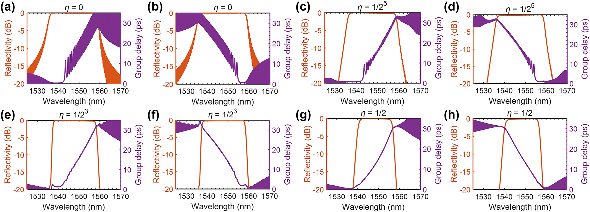
Simulated transmission spectra and group delay spectra of a 2-mm-long CMWG under different apodization length ratio η. (a) η = 0 at positive state; (b) η = 0 at negative state; (c) η = 1/25 at positive state; (d) η = 1/25 at negative state; (e) η = 1/23 at positive state; (f) η = 1/23 at negative state; (g) η = 1/2 at positive state; (h) η = 1/2 at negative state.
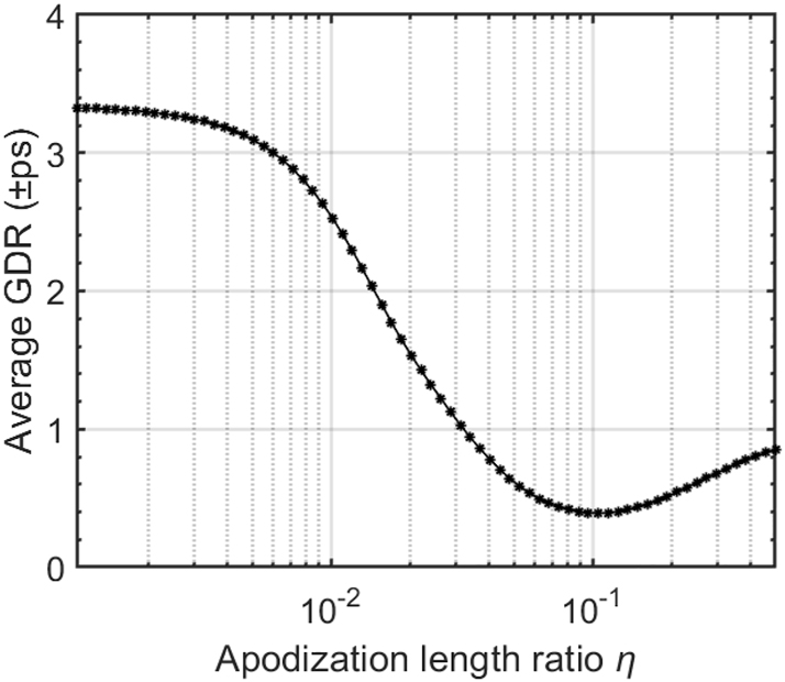
Calculated average GDR as the apodization length ratio η varies.
Figure 4(a)–(d) show the calculated results of the transmission spectra and group delays for the case with positive and negative dispersions in cascade. It can be seen that larger group delay leads to higher loss, which is intrinsically due to the longer propagation distance involved. This manifests as increased loss at the longer wavelengths for the case with positive dispersion or at the shorter wavelengths for the case with negative dispersion. When the number of the cascaded CMWGs is given as N = 1, 2, 4, 8, 16, 32, and 64, the accumulated dispersion is 1.8, 3.6, 7.2, 14.5, 28.9, 57.8, and 115.7 ps/nm, respectively, for the case of producing the positive dispersion. Similarly, the corresponding negative dispersion is −1.7, −3.4, −6.7, −13.4, −26.9, −53.8, and −107.5 ps/nm, respectively, when there are 1, 2, 4, 8, 16, 32, and 64 CMWGs involved. Moreover, the positive dispersion is slightly higher than the negative dispersion, which can be explained as follows. First, the group delay is not dependent linearly on the wavelength due to the nonlinear varying of the mode effective index along the CMWG [32]. Second, a portion of the front part of the CMWG does not contribute to the group delay, corresponding to short wavelengths in the positive state and long wavelengths in the negative state. This is similar to the detailed analysis for silicon CMWGs discussed in our previous work [19]. As a result, the slope of the group-delay spectrum for positive dispersion is larger than that for negative dispersion, leading to stronger dispersion.
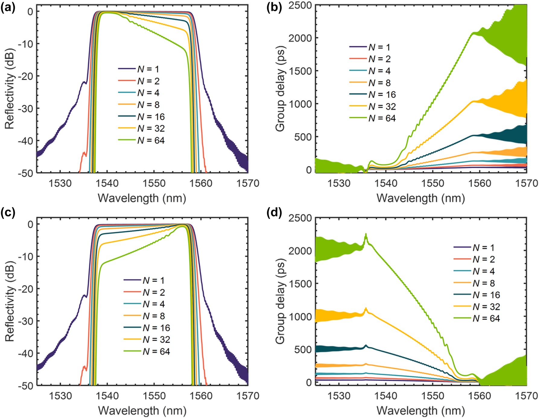
Simulated transmission spectra and group delay spectra as the cascaded number N increases. (a) Simulated transmission spectra as the cascaded number N increases at positive state; (b) simulated group delay spectra as the cascaded number N increases at positive state; (c) simulated transmission spectra as the cascaded number N increases at negative state; (b) simulated group delay spectra as the cascaded number N increases at negative state.
3 Fabrication and measurement
The designed dispersion compensator was fabricated on an X-cut TFLN wafer with a 400-nm-thick layer and a 1.1-μm-thick buried oxide layer. The waveguide was patterned by using an electron beam lithography (EBL) process, and the LN layer was etched with a depth of 200 nm through an optimized Ar-gas-based ICP process. Figure 5(a) shows the microscope image of the fabricated positive/negative dispersion compensators with different cascaded numbers of N = 2, 4, 8, 16, and 32. Figure 5(b)–(e) show the scanning electron microscopic (SEM) images of the key elements including grating coupler, mode (de)multiplexer, and grating corrugations. Here, grating couplers for TE-polarization were used to provide the convenience for chip-fiber coupling. By using the 2-mm-long CMWGs, the total length for the dispersion compensator is 4.65 mm, and the lateral separation between two adjacent CMWG is 5 μm. The width of the dispersion compensator with two CMWGs in cascade is 48 μm, while the width increases by 7.5 μm when a pair of CMWGs is further cascaded. As a result, the width of the dispersion compensator with 32 CMWGs in cascade is 160.5 μm, showing very high footprint compactness.
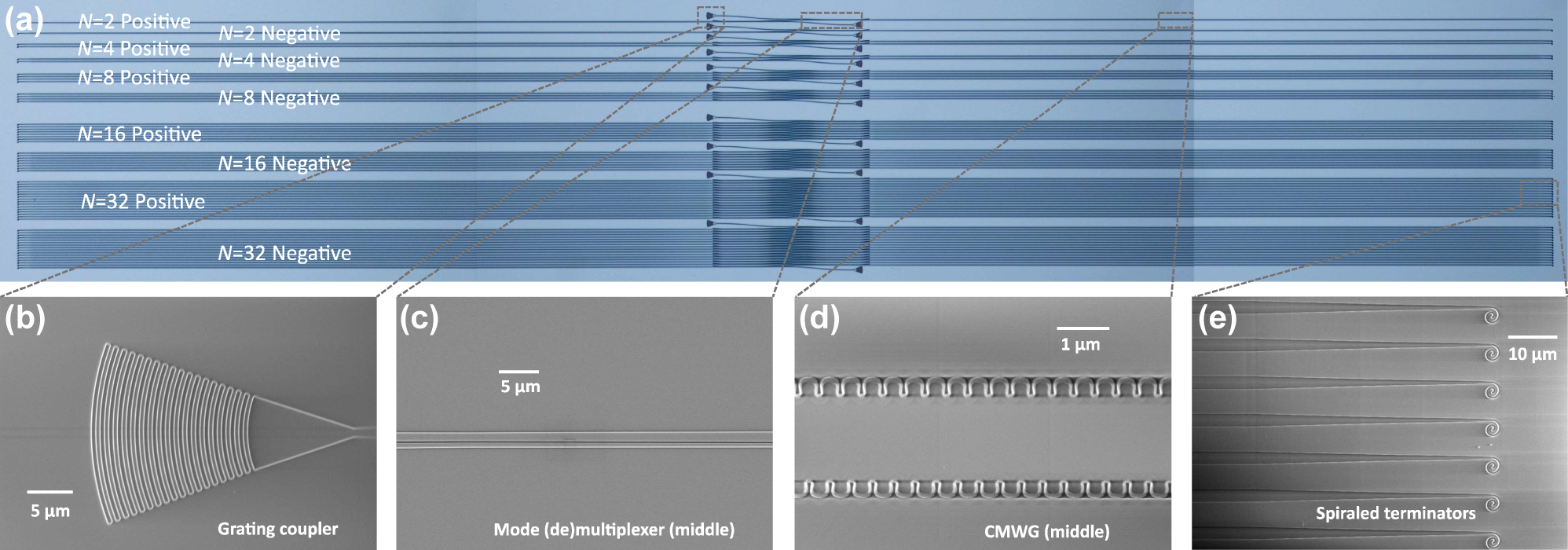
Microscope and SEM images. (a) Microscope image of the fabricated dispersion compensator composed of CMWGs in zigzag-cascade; (b–d) SEM images of the grating coupler (b), the mode (de)multiplexer (c), and the grating corrugations (d).
An optical spectrum analyzer (OSA) was used to measure the spectral responses. The measured results were normalized with respect to the transmission of a 500-μm-long straight waveguide on the same chip. Figure 6(a) and (b) shows the measured reflectivity responses with different numbers of the CMWG in cascade (i.e., N = 2, 4, 8, 16, and 32), including the cases with positive/negative dispersion. As it can be seen, the excess loss caused by mode (de)multiplexers is less than 1 dB for each CMWG, and the reflectivity bandwidth of a CMWG is about 21 nm as expected. The group delays were measured by detecting the output signal by using a digital communication analyzer (DCA). Here light was modulated by a 10-GHz radio frequency signals before injecting into the dispersion compensator. Figure 6(c) and (d) show the measured group delays as the CMWG numbers N increases for the cases with positive and negative dispersion, respectively. From the linear fitting in the wavelength range of 1,544–1,558 nm, the measured positive dispersion is estimated as 3.8, 7.2, 12.2, 26.2, and 49.2 ps/nm when N = 2, 4, 8, 16, and 32, while the corresponding GDR is ±2.17, ±4.26, ±8.40, ±15.44, and ±17.98 ps. From Figure 6(d), the negative dispersion is about −2.7, −5.6, −10.9, −20.5, and −39.3 ps/nm for the cases with N = 2, 4, 8, 16, and 32, while the GDR is ±1.90, ±3.88, ±6.19, ±9.40, ±18.69 ps. Accordingly, the average dispersion produced by a CMWG is +1.5 ps/nm and −1.2 ps/nm. When there are 32 CWMGs in cascade, the maximal group delay reaches 781.8 ps and −728.1 ps, while the GDR suppression is excellent, enabling that the GDR is only 2.5 % of the total group delay. Here, larger propagation distance brings higher loss. The maximal total losses for positive and negative dispersions are −13 dB and −17 dB at the longest and shortest wavelength-sides, respectively. Furthermore, we evaluate the propagation loss for the present dispersion compensator, as given in Figure 6(e), showing that the average loss of each CMWG is fitted as 0.188 dB, corresponding to an average propagation loss of 0.47 dB/cm. Moreover, the thermo-optic coefficient of TFLN (∼10−5 K−1) is much lower than silicon, showing higher robustness to the environment temperature variation [33].
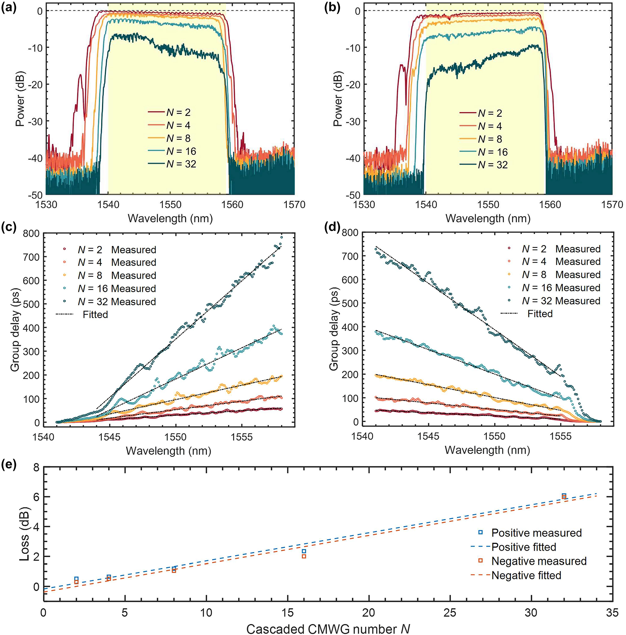
Measured results. (a, b) Measured transmission spectra as the cascaded number N increases with positive (a) and negative (b) dispersion; (c, d) measured group delay spectra as the cascaded number N increases with positive (c) and negative (d) dispersion; (e) propagation loss for different cascaded CMWG number N with positive/negative dispersion production.
Finally, the present dispersion compensator was used to compensate the positive dispersion produced by a 5-km-long SMF when transmitting 40 Gbps OOK signals, as shown in Figure 7. Here the used standard SMF-28 has a dispersion of less than 18 ps/nm/km. Figure 7(a) shows the measured eye diagrams when the signals go through a straight TFLN photonic waveguide, featuring a signal-to-noise ratio (SNR) of 6.4 dB. When the SMF is added before the chip coupler, the eye-diagrams became highly blurred where the SNR is too low to detect due to the dispersion in the SMF, as shown in Figure 7(b). When introducing the present negative compensator with N = 32 in the system, the eye diagrams measured for the operation wavelengths of 1,545, 1,548, 1,551, 1,554, and 1,557 nm show great improvement with SNRs as high as 6.0 dB, as shown in Figure 7(c)–(g). One should note that, the eye diagram is getting blurred when the operation wavelength is less than 1,545 nm due to the noise caused by high loss at the shorter wavelength when operating with negative dispersion.
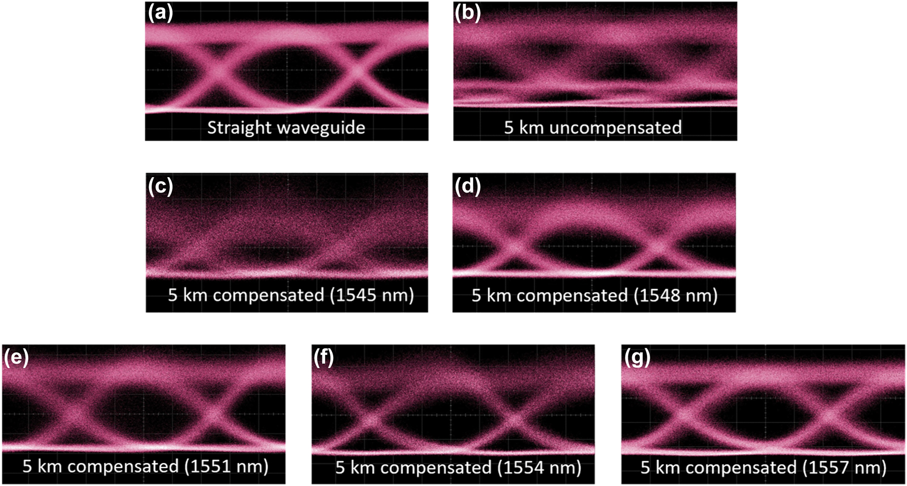
Measured eye diagrams of 40 Gbps OOK signals. (a) Straight waveguide only; (b) straight waveguide with a 5-km-long SMF added before; (c–g) post-compensated 5-km-long SMF at 1,545 (c), 1,548 (d), 1,551 (e), 1,554 (f), and 1,557 nm (g).
4 Conclusions
In conclusion, we have presented the first circulator-free TFLN dispersion compensator consisting of multiple CMWGs in zigzag-cascade, while optical circulators are eliminated with the assistance of mode (de)multiplexers. The present configuration has the big advantage of being ultra-compact and has addressed the issue of being unable to use spiral TFLN CMWG for footprint compactness. By introducing straight CMWGs in zigzag-cascade, the proposed dispersion compensator is ultra-compact and highly scalable. In particular, positive or negative dispersion has been achieved by selecting the input ports appropriately. In our experiments, each CMWG produces a dispersion of +1.5 ps/nm or −1.2 ps/nm, while the maximal dispersion of +49.2 ps/nm and −39.3 ps/nm is produced within a 21-nm-wide wavelength range, for the dispersion compensator with 32 CMWGs in zigzag-cascade. The proposed zigzag-cascade structure is highly scalable, where loss is indeed the key limitation. The measurement results have shown that the propagation loss is as low as 0.47 dB/cm, which is much lower than that of silicon CMWGs (e.g., >1.5 dB/cm). Moreover, the dispersion compensator was utilized to compensate the dispersion introduced by a 5-km-long SMF in a data-transmission link with 40 Gbps OOK signals, demonstrating the excellence of the present on-chip dispersion compensation. As a conclusion, the present dispersion compensator is highly scalable and provides a promising way for advanced photonic systems necessitating dispersion management, such as high-speed optical interconnects in datacenters.
Funding source: National Natural Science Foundation of China
Award Identifier / Grant number: 62321166651
Award Identifier / Grant number: 92150302
Award Identifier / Grant number: U23B2047
Funding source: the Leading Innovative and Entrepreneur Team Introduction Program of Zhejiang
Award Identifier / Grant number: 2021R01001
Funding source: National Major Research and Development Program
Award Identifier / Grant number: 2019YFB2203603
Funding source: Zhejiang Provincial Major Research and Development Program
Award Identifier / Grant number: 2021C01199
Funding source: the Fundamental Research Funds for the Central Universities
Award Identifier / Grant number: 2021QNA5002
Funding source: Zhejiang Postdoctoral Science Foundation
Award Identifier / Grant number: ZJ2022101
-
Research funding: This work was supported by National Major Research and Development Program (No. 2019YFB2203603), National Natural Science Foundation of China (NSFC) (62321166651, U23B2047, 92150302), Zhejiang Provincial Major Research and Development Program (No. 2021C01199), the Fundamental Research Funds for the Central Universities (2021QNA5002), the Leading Innovative and Entrepreneur Team Introduction Program of Zhejiang (2021R01001), and Zhejiang Postdoctoral Science Foundation (ZJ2022101).
-
Author contributions: All authors have accepted responsibility for the entire content of this manuscript and approved its submission.
-
Conflict of interest: Authors state no conflict of interest.
-
Data availability: The datasets generated and analysed during the current study are available from the corresponding author upon reasonable request.
References
[1] D. Perez, I. Gasulla, and J. Capmany, “Toward programmable microwave photonics processors,” J. Lightwave Technol., vol. 36, no. 2, pp. 519–532, 2018. https://doi.org/10.1109/jlt.2017.2778741.Suche in Google Scholar
[2] Y. Han, S. Shi, R. Jin, Y. Wang, and Q. Qiu, “Integrated waveguide true time delay beamforming system based on an SOI platform for 28 GHz millimeter-wave communication,” Appl. Opt., vol. 59, no. 26, pp. 7770–7778, 2020. https://doi.org/10.1364/ao.397202.Suche in Google Scholar
[3] A. Rashidinejad, Y. Li, and A. M. Weiner, “Recent advances in programmable photonic-assisted ultrabroadband radio-frequency arbitrary waveform generation,” IEEE J. Quantum Electron., vol. 52, no. 1, pp. 1–17, 2016. https://doi.org/10.1109/jqe.2015.2506987.Suche in Google Scholar
[4] J. Leuthold, C. Koos, and W. Freude, “Nonlinear silicon photonics,” Nat. Photonics, vol. 4, no. 8, pp. 535–544, 2010. https://doi.org/10.1038/nphoton.2010.185.Suche in Google Scholar
[5] G. Chen, et al.., “Advances in lithium niobate photonics: development status and perspectives,” Adv. Photonics, vol. 4, no. 3, 2022, Art. no. 034003. https://doi.org/10.1117/1.ap.4.3.034003.Suche in Google Scholar
[6] D. Zhu, et al.., “Integrated photonics on thin-film lithium niobate,” Adv. Opt. Photonics, vol. 13, no. 2, pp. 242–352, 2021. https://doi.org/10.1364/aop.411024.Suche in Google Scholar
[7] B. Chen, et al.., “Low-loss fiber grating coupler on thin film lithium niobate platform,” APL Photonics, vol. 7, no. 7, 2022, Art. no. 076103. https://doi.org/10.1063/5.0093033.Suche in Google Scholar
[8] J. Ling, Y. He, R. Luo, M. Li, H. Liang, and Q. Lin, “Athermal lithium niobate microresonator,” Opt. Express, vol. 28, no. 15, pp. 21682–21691, 2020. https://doi.org/10.1364/oe.398363.Suche in Google Scholar
[9] D. Pohl, F. Kaufmann, M. R. Escalé, J. Holzer, and R. Grange, “Tunable Bragg grating filters and resonators in lithium niobate-on-insulator waveguides,” in Conference on Lasers and Electro-Optics, Washington, DC, Optica Publishing Group, 2020, p. STu4J.5.10.1364/CLEO_SI.2020.STu4J.5Suche in Google Scholar
[10] W. Ke, et al.., “Digitally tunable optical delay line based on thin-film lithium niobate featuring high switching speed and low optical loss,” Photonics Res., vol. 10, no. 11, pp. 2575–2583, 2022. https://doi.org/10.1364/prj.471534.Suche in Google Scholar
[11] Z. Li, et al.., “High density lithium niobate photonic integrated circuits,” Nat. Commun., vol. 14, no. 1, p. 4856, 2023. https://doi.org/10.1038/s41467-023-40502-8.Suche in Google Scholar PubMed PubMed Central
[12] M. Yu, et al.., “Integrated femtosecond pulse generator on thin-film lithium niobate,” Nature, vol. 612, no. 7939, pp. 252–258, 2022. https://doi.org/10.1038/s41586-022-05345-1.Suche in Google Scholar PubMed
[13] A. Waqas, D. Melati, and A. Melloni, “Cascaded Mach–Zehnder architectures for photonic integrated delay lines,” IEEE Photonics Technol. Lett., vol. 30, no. 21, pp. 1830–1833, 2018. https://doi.org/10.1109/lpt.2018.2865703.Suche in Google Scholar
[14] R. Moreira, S. Gundavarapu, and D. J. Blumenthal, “Programmable eye-opener lattice filter for multi-channel dispersion compensation using an integrated compact low-loss silicon nitride platform,” Opt. Express, vol. 24, no. 15, pp. 16732–16742, 2016. https://doi.org/10.1364/oe.24.016732.Suche in Google Scholar
[15] H. Sun, L. Lu, Y. Liu, Z. Ni, J. Chen, and L. Zhou, “Broadband 1×8 optical beamforming network based on anti-resonant microring delay lines,” J. Lightwave Technol., vol. 40, no. 20, pp. 6919–6928, 2022. https://doi.org/10.1109/jlt.2022.3175768.Suche in Google Scholar
[16] V. Sorianello, et al.., “100Gb/s PolMux-NRZ transmission at 1550nm over 30km single mode fiber enabled by a silicon photonics optical dispersion compensator,” in Optical Fiber Communication Conference, San Diego, California, Optica Publishing Group, 2018, p. W2A.31.10.1364/OFC.2018.W2A.31Suche in Google Scholar
[17] X. Wang, Y. Zhao, Y. Ding, S. Xiao, and J. Dong, “Tunable optical delay line based on integrated grating-assisted contradirectional couplers,” Photonics Res., vol. 6, no. 9, pp. 880–886, 2018. https://doi.org/10.1364/prj.6.000880.Suche in Google Scholar
[18] W. Shi, V. Veerasubramanian, D. Patel, and D. V. Plant, “Tunable nanophotonic delay lines using linearly chirped contradirectional couplers with uniform Bragg gratings,” Opt. Lett., vol. 39, no. 3, pp. 701–703, 2014. https://doi.org/10.1364/ol.39.000701.Suche in Google Scholar PubMed
[19] S. Liu, R. Ma, Z. Yu, Y. Shi, and D. Dai, “On-chip digitally tunable positive/negative dispersion controller using bidirectional chirped multimode waveguide gratings,” Adv. Photonics, vol. 5, no. 6, 2023, Art. no. 066005. https://doi.org/10.1117/1.ap.5.6.066005.Suche in Google Scholar
[20] I. Giuntoni, D. Stolarek, J. Bruns, L. Zimmermann, B. Tillack, and K. Petermann, “Integrated dispersion compensator based on apodized SOI Bragg gratings,” IEEE Photonics Technol. Lett., vol. 25, no. 14, pp. 1313–1316, 2013. https://doi.org/10.1109/lpt.2013.2264050.Suche in Google Scholar
[21] Y. Liu, L. Lu, Z. Ni, J. Chen, J. Chen, and L. Zhou, “Silicon integrated continuously tunable dispersion compensator based on cascaded micro-ring resonators,” in Asia Communications and Photonics Conference (ACP), 2022.10.1109/ACP55869.2022.10088552Suche in Google Scholar
[22] B. Pan, Y. Tan, P. Chen, L. Liu, Y. Shi, and D. Dai, “Compact racetrack resonator on LiNbO3,” J. Lightwave Technol., vol. 39, no. 6, pp. 1770–1776, 2021. https://doi.org/10.1109/jlt.2020.3040387.Suche in Google Scholar
[23] A. D. White, et al.., “Integrated passive nonlinear optical isolators,” Nat. Photonics, vol. 17, no. 2, pp. 143–149, 2022. https://doi.org/10.1038/s41566-022-01110-y.Suche in Google Scholar
[24] Y. Sun, et al.., “Large group delay in silicon-on-insulator chirped spiral Bragg grating waveguide,” IEEE Photonics J., vol. 13, no. 5, pp. 1–5, 2021. https://doi.org/10.1109/jphot.2021.3112719.Suche in Google Scholar
[25] Z. Du, et al.., “Silicon nitride chirped spiral Bragg grating with large group delay,” APL Photonics, vol. 5, no. 10, 2020, Art. no. 101302. https://doi.org/10.1063/5.0022963.Suche in Google Scholar
[26] Y. Li, L. Xu, D. Wang, Q. Huang, C. Zhang, and X. Zhang, “Large group delay and low loss optical delay line based on chirped waveguide Bragg gratings,” Opt. Express, vol. 31, no. 3, pp. 4630–4638, 2023. https://doi.org/10.1364/oe.480375.Suche in Google Scholar PubMed
[27] S. Liu, C. Zhang, H. Cao, S. Hong, Z. Yu, and D. Dai, “On-chip circulator-free chirped spiral multimode waveguide grating for dispersion management,” ACS Photonics, vol. 10, no. 5, pp. 1654–1661, 2023. https://doi.org/10.1021/acsphotonics.3c00326.Suche in Google Scholar
[28] G. Chen, et al.., “Compact 100GBaud driverless thin-film lithium niobate modulator on a silicon substrate,” Opt. Express, vol. 30, no. 14, 2022. https://doi.org/10.1364/oe.458431.Suche in Google Scholar PubMed
[29] W. Zhao, et al.., “High‐performance mode‐multiplexing device with anisotropic lithium‐niobate‐on‐insulator waveguides,” Laser Photonics Rev., vol. 17, no. 5, 2023, Art. no. 2200774. https://doi.org/10.1002/lpor.202200774.Suche in Google Scholar
[30] L. Poladian, “Understanding profile-induced group-delay ripple in Bragg gratings,” Appl. Opt., vol. 39, no. 12, pp. 1920–1923, 2000. https://doi.org/10.1364/ao.39.001920.Suche in Google Scholar PubMed
[31] G. W. Chern and L. A. Wang, “Transfer-matrix method based on perturbation expansion for periodic and quasi-periodic binary long-period gratings,” J. Opt. Soc. Am. A, vol. 16, no. 11, pp. 2675–2689, 1999. https://doi.org/10.1364/josaa.16.002675.Suche in Google Scholar
[32] X. Gao, et al.., “Integrated contra-directionally coupled chirped Bragg grating waveguide with a linear group delay spectrum,” Front. Optoelectron., vol. 16, no. 1, p. 6, 2023. https://doi.org/10.1007/s12200-023-00061-8.Suche in Google Scholar PubMed PubMed Central
[33] L. Moretti, M. Iodice, F. G. Della Corte, and I. Rendina, “Temperature dependence of the thermo-optic coefficient of lithium niobate, from 300 to 515 K in the visible and infrared regions,” J. Appl. Phys., vol. 98, no. 3, 2005. https://doi.org/10.1063/1.1988987.Suche in Google Scholar
© 2024 the author(s), published by De Gruyter, Berlin/Boston
This work is licensed under the Creative Commons Attribution 4.0 International License.
Artikel in diesem Heft
- Frontmatter
- Review
- Plasmon-driven molecular scission
- Research Articles
- Ultra-compact thin-film-lithium-niobate photonic chip for dispersion compensation
- Optimization of NC-LSPR coupled MoS2 phototransistors for high-performance broad-spectrum detection
- Impact of temperature on the brightening of neutral and charged dark excitons in WSe2 monolayer
- Designing rotational motion of charge densities on plasmonic nanostructures excited by circularly polarized light
- Twist-tunable in-plane anisotropic polaritonic crystals
- An overview on plasmon-enhanced photoluminescence via metallic nanoantennas
- Unique features of plasmonic absorption in ultrafine metal nanoparticles: unity and rivalry of volumetric compression and spill-out effect
- Constant-force photonic projectile for long-distance targeting delivery
- Emission dynamics and spectrum of a nanoshell-based plasmonic nanolaser spaser
- Degeneracy mediated thermal emission from nanoscale optical resonators with high-order symmetry
- Erratum
- Corrigendum to: modeling with graded interfaces: tool for understanding and designing record-high power and efficiency mid-infrared quantum cascade lasers