Guiding light with surface exciton–polaritons in atomically thin superlattices
-
Sara A. Elrafei
 ,
Sandra de Vega
,
Sandra de Vega


Abstract
Two-dimensional materials give access to the ultimate physical limits of photonics with appealing properties for ultracompact optical components such as waveguides and modulators. Specifically, in monolayer semiconductors, a strong excitonic resonance leads to a sharp oscillation in permittivity from positive to even negative values. This extreme optical response enables surface exciton–polaritons to guide visible light bound to an atomically thin layer. However, such ultrathin waveguides support a transverse electric (TE) mode with low confinement and a transverse magnetic (TM) mode with short propagation. Here, we propose that realistic semiconductor–insulator–semiconductor superlattices comprising monolayer WS2 and hexagonal boron nitride (hBN) can improve the properties of both TE and TM modes. Compared to a single monolayer, a heterostructure with a 1-nm hBN spacer separating two monolayers enhances the confinement of the TE mode from 1.2 to around 0.5 μm, while the out-of-plane extension of the TM mode increases from 25 to 50 nm. We propose two simple additivity rules for mode confinement valid in the ultrathin film approximation for heterostructures with increasing spacer thickness. Stacking additional WS2 monolayers into superlattices further enhances the waveguiding properties. Our results underscore the potential of monolayer-based superlattices as a platform for visible-range nanophotonics with promising optical, electrical, and magnetic tunability.
1 Introduction
Surface polaritons are electromagnetic surface waves that can mediate enhanced light–matter interaction at the nanoscale. They are crucial for developing highly miniaturized and efficient optical devices such as modulators, sensors, light sources, and photodetectors. These waves propagate along the interface between two materials and decay in the perpendicular (out-of-plane) direction. Surface polaritons can be sustained by different types of quasiparticles in matter, like plasmons in metals, phonons in insulators, and excitons in semicoductors [1]. Noble metals are common materials for supporting surface plasmon–polaritons and guiding light below the diffraction limit due to their strong light confinement capability [2], [3]. However, active tunability remains elusive because it is difficult to substantially alter the high density of free electrons in a metal.
Compared to plasmon–polaritons, surface exciton–polaritons (SEPs) are excitons that concomitantly oscillate with photons, producing a propagating surface wave bound to the interface. Exciton–polaritons have been experimentally observed in different organic [4], [5] and inorganic crystals [6], [7] with large absorption coefficients. For example, molecular J-aggregates of organic dyes [8], [9] can sustain SEPs at room temperature and create opportunities to realize novel sensors [10]. However, SEPs in those materials still have tunability limitations. As an alternative, atomically thin materials possess extreme optical properties that can be modulated while potentially giving access to the spin and valley degrees of freedom in their electronic band structures [11], [12]. Graphene and hexagonal boron nitride can indeed support plasmon– and phonon–polaritons, including modes with appealing properties such as hyperbolic polaritons that emerge due to optical anisotropy [1], [13], [14], [15], [16]. These polaritons occur, however, at terahertz and mid-infrared frequencies [17], [18].
In the visible spectral range, semiconductor monolayers of transition metal dichalcogenides (TMDs) such as WS2 are good candidates for guiding light using SEPs. TMD monolayers host excitons with a high oscillator strength, producing a dramatic permittivity oscillation around the exciton energy [19]. As a result, excitons in TMDs can strongly reflect electromagnetic radiation and act as atomically thin mirrors [20], [21], [22]. Interestingly, excitons can be tuned electrically, optically, magnetically, thermally, or mechanically [22], [23], [24], [25], [26], opening a promising avenue for active nanophotonic devices. Several theoretical works have dealt with the excitation of SEPs in monolayers and their coupling to nearby emitters [26], [27], [28]. A report proposed that a monolayer could support SEPs and predicted confinement to within 2 μm of the monolayer with propagation lengths exceeding 100 μm [29]. Although the near-zero thickness of the monolayer can support waveguide modes, they are loosely confined to the TMD monolayer and require a symmetric refractive-index environment. One possibility to increase confinement is patterning the monolayer into a photonic crystal, which has been demonstrated for suspended structures [30]. For unpatterned monolayers, however, the proximity of the guided mode to the light line complicates experimental detection due to the requirement for a perfectly symmetric optical environment with low scattering [31]. Furthermore, detection relies critically on achieving narrow excitonic linewidths, which can require cryogenic temperatures [32].
Here, we address the fundamental challenge of guiding light bound to atomically thin semiconductors. We propose van der Waals superlattices based on semiconductor–insulator–semiconductor heterostructures to improve the propagation characteristics of surface exciton–polaritons (Figure 1(a)). We show the existence of both TE and TM guided modes and compare their dispersion relations in monolayers, heterostructures, and superlattices made of monolayer WS2 and hexagonal boron nitride. Compared to negligible confinement in a monolayer, we demonstrate increased confinement of the TE mode in heterostructures. Then, we clarify the impact of the thickness of the spacer layer on the guided modes. In the ultrathin film approximation, we find that the decay constants of the TE and TM modes supported by heterostructures follow simple additivity rules for their constituent layers. Additionally, we investigate the electrostatic tuning of the modes. To guide experimental realizations under different excitation conditions, we investigate the differences between two approaches for solving the mode dispersions of the superlattices using either a complex in-plane wave vector, β, or a complex frequency, ω. Our study thus produces specific directions to tailor and tune guided modes in semiconductor monolayer superlattices as a platform for nanoscale photonic and optoelectronic devices.
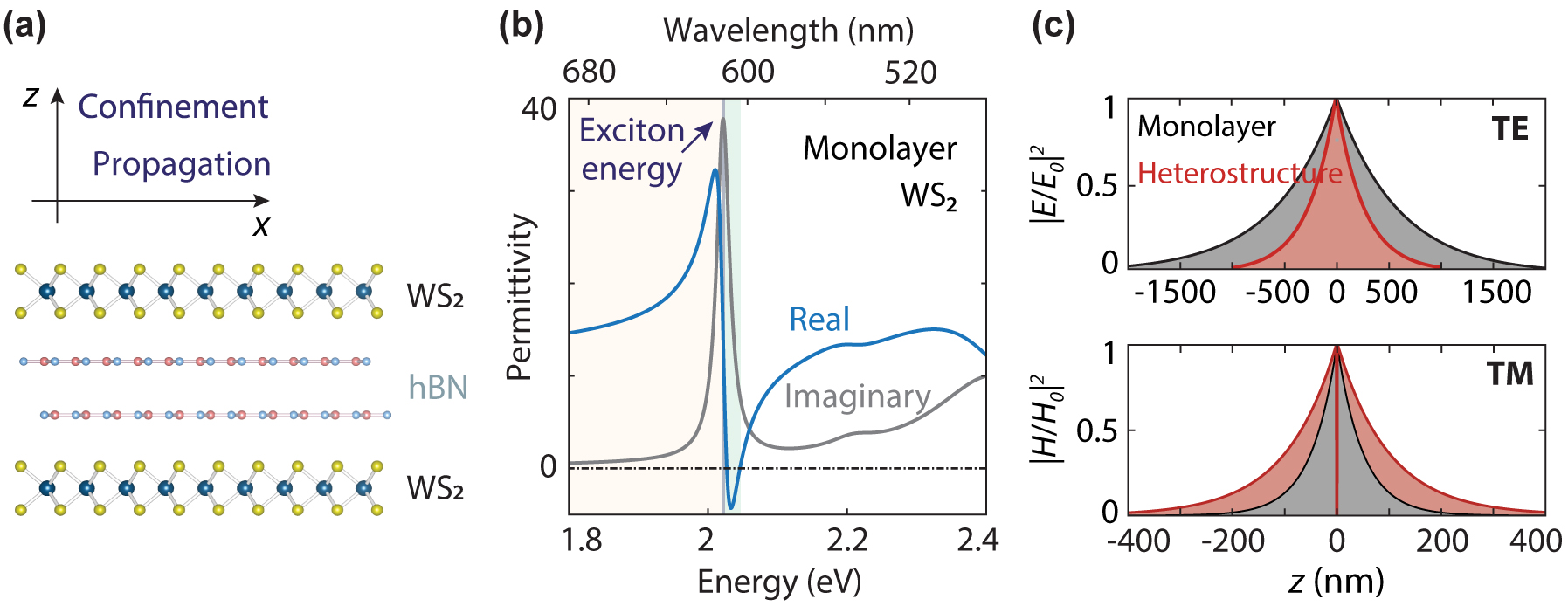
Waveguiding in WS2 monolayers around a permittivity oscillation due to a high exciton oscillator strength. (a) Atomically thin semiconductor–insulator–semiconductor heterostructure with a hexagonal boron nitride spacer in a symmetric refractive-index environment. (b) Experimentally retrieved permittivity of monolayer WS2 obtained by fitting a transmission spectrum using the transfer-matrix method and a permittivity model with 4 Lorentzians. TE or TM modes can be supported depending on the sign of the real part of the permittivity in the yellow and green areas, respectively. (c) Electric and magnetic field profiles for the modes guided by a monolayer (black) and a heterostructure with a spacer thickness of 1 nm (red) at energies of 2 and 2.0223 eV. The field is confined in the out-of-plane direction, while the waves propagate in the plane. Heterostructures contribute to increased confinement of the TE mode and reduced confinement of the TM mode.
2 Strong exciton oscillator strength and permittivity
We use WS2 monolayers due to their strong exciton oscillator strength and narrow linewidth, which are better than in other semiconductors at room temperature and result in a record absorption coefficient. To retrieve the permittivity of a realistic, high-quality monolayer, we deposit a mechanically exfoliated WS2 monolayer on polydimethylsiloxane (PDMS) on a glass substrate. Using PDMS as a substrate facilitates a narrow and strong exciton peak while preserving the quantum efficiency of the monolayer emission [33]. Transmittance spectroscopy shows a strong excitonic resonance with approximately 17 % transmittance contrast and a narrow exciton linewidth, γ
A
= 22.7 meV (Supplementary Section S1). We fit the measured transmission spectrum using transfer-matrix analysis and model the in-plane permittivity of monolayer WS2 with 4 Lorentzian oscillators [19], [34], [35] as
The permittivity oscillation around the exciton energy in Figure 1(b) is so pronounced that the real part of the permittivity, Re{ε}, goes from positive to negative across the excitonic resonance. Effectively, the material behaves optically like a high-refractive-index dielectric when Re{ε} > 0 or a reflective metal when Re{ε} < 0. These permittivities facilitate two regimes for guiding SEP waves: a TE mode can be supported in the range of positive and high real permittivity (above 612.5 nm, orange area), while a TM mode can be sustained where the condition Re{ε} + Re{ε medium} < 0 is met (from 606.5 to 612.5 nm, green area).
3 Surface exciton–polaritons in monolayers and heterostructures
We consider a semiconductor monolayer as a thin film of thickness t = 0.618 nm with permittivity ε
m
cladded between two homogenous media with refractive indices n
1 and n
2. For simplicity in our analysis, we consider an isotropic thin-film model for WS2 to represent the material optical response. Such a layered medium can support TE and TM modes. To support a guided mode in monolayer WS2, however, the environment refractive index must be nearly symmetric with n
1 ∼ n
2. Otherwise, a cutoff appears in the minimum required TMD thickness (Supplementary Section S2). To study the mode propagation characteristics, we base our calculations on the transfer-matrix method (see Methods) [36], [37]. Through iterative transfer-matrix-method simulations using the dielectric responses of the involved materials, we model the SEP dispersion characteristics within our heterostructures. Specifically, the matrix element M
22 must be zero for a guided mode. We solve the equations numerically in the complex-ω plane to obtain the real in-plane wave vector β of the supported guided mode (Supplementary Section S3) and evaluate its effective width W
eff = 1/Re{q} and effective SEP wavelength λ
SEP = 2π/Re{β}, where
We use this method first to show that a WS2 monolayer can support SEP modes at energies close to the exciton. SEP waves propagate along the monolayer and decay evanescently in the perpendicular direction (z axis in Figure 1(a)). TE and TM modes can be excited in different energy ranges depending on the sign of the permittivity. The TE mode is only supported when Re{ε
m
} > 0, while the TM mode starts to appear as the sign of the permittivity changes to negative (Figure 1(b), yellow and green areas). The TE mode of a monolayer is very close to the light line (Figure 2(a), black), with an effective refractive index close to the surrounding medium. Near the exciton energy
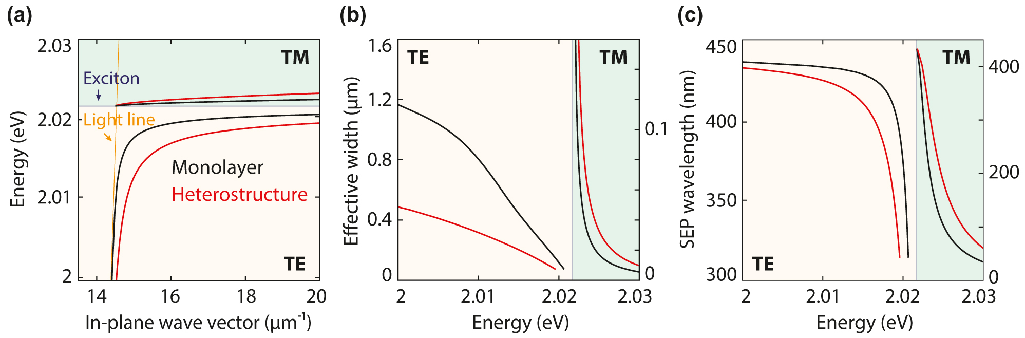
Guided modes for a WS2 monolayer and a WS2-hBN-WS2 heterostructure. The stack has a spacer thickness of 1 nm and is embedded in a symmetric PDMS environment. (a) Dispersion relation for the TE (yellow area) and TM (green) modes in a WS2 monolayer (black) and a heterostructure with 1-nm-thick hBN spacer (red) calculated using the complex-ω approach. Compared to the light line (orange shaded line), the TE mode is more confined in the heterostructure than in a single monolayer, while the TM mode becomes less confined. (b) Effective width of the guided modes. (c) Exciton–polariton wavelength as a function of photon energy.
To overcome the confinement challenges predicted for the WS2 monolayer, we introduce a hexagonal boron nitride (hBN) layer between two WS2 monolayers. We approximate the refractive index of hBN as isotropic, setting it to 2.3 in our simulations. Although hBN is an anisotropic material [38], [39], its birefringence would only lead to minor modifications in our study. In general, the introduction of an hBN spacer layer significantly alters the dispersion relation of the TE and TM modes. In this heterostructure, the bending of the dispersion curve starts further away from the exciton energy compared to the monolayer and evolves more slowly with energy (Figure 2(a), red). This enhanced mode confinement facilitates experimental observation because otherwise loosely bound guided waves are easily scattered by imperfections.
The mode profiles for a WS2 monolayer (Figure 1(c), black lines) and a heterostructure (red) for the TE and TM modes at energies of 2 and 2.0223 eV, respectively, illustrate optical confinement close to the monolayer. All modes show evanescent behavior outside the waveguide core, with the TM mode being more confined than the TE mode. Using a heterostructure with an hBN spacer thickness of 1 nm also reshapes the waveguiding characteristics. When transitioning from a monolayer to a heterostructure at an energy of 2 eV, the effective width of the TE mode is compressed from 1.2 to approximately 0.5 µm (Figure 2(b)). For the TM mode at energies above the exciton peak, the mode exhibits the opposite behavior and becomes less tightly confined, with the TM-mode effective width increasing from 47 to 90 nm for a heterostructure at an energy of 2.023 eV.
4 Contribution of the spacer to confinement
In heterostructures, the confinement of the guided mode depends on the insulator spacer thickness. Increasing the spacer thickness typically increases the propagation constant of the TE mode. Furthermore, the TM dispersion line moves toward the monolayer curve. To gain insight into these modes, we evaluate the intensity modal profile for heterostructures with varying spacer thickness (Figure 3(a)). The confinement of the TE mode at E = 2 eV is enhanced by an order of magnitude as the spacer thickness goes from 1 to 100 nm. The TE mode shifts to higher β as the spacer thickness increases, resulting in a more confined SEP width and a shorter SEP wavelength (Figure 3(b) and (c)). This apparent confinement is, however, due to the introduction of a material with a higher refractive index than the surrounding medium, which shifts the dispersion curve away from the PDMS light line toward that of the spacer material. Similarly, for the TM mode, increasing the spacer thickness reduces the width, resulting in higher confinement and shortening of the SEP wavelength (Figure 3(b) and (c)). Note that the TM-mode intensity profile at E = 2.0223 eV (Figure 3(a)) corresponds to an antisymmetric electric field distribution (Supplementary Section S4).
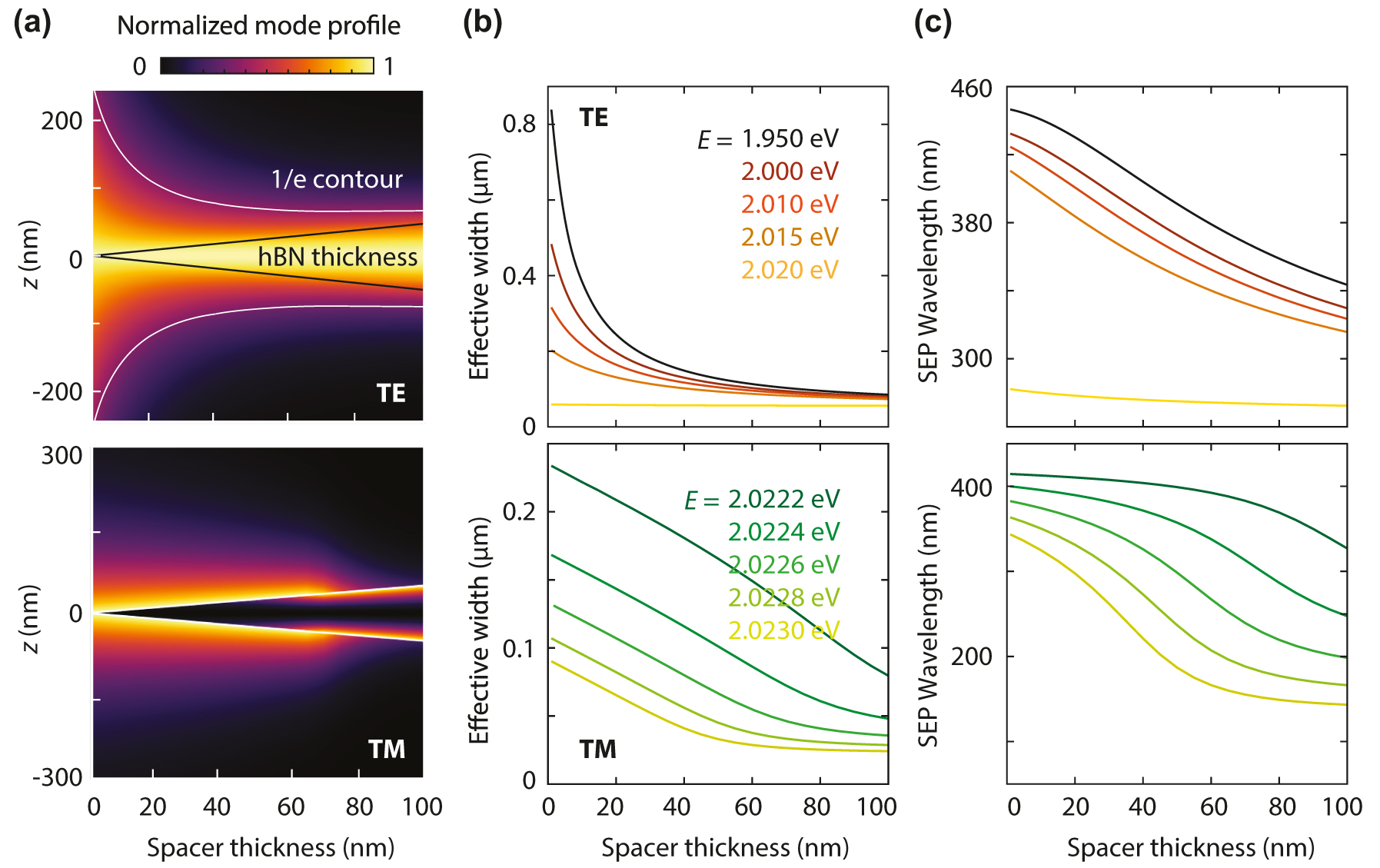
Guided-mode properties in a heterostructure as a function of spacer thickness. (a) Electric-field intensity profile for increasing spacer thickness in the TE mode at a photon energy of 2 eV and in the TM mode at 2.0223 eV. The dark-gray lines indicate the hBN thickness. The white contour line identifies confinement for 1/e intensity decay. (b) TE- and TM-mode effective width at different energies demonstrating the contribution of the spacer thickness to confinement. (c) Corresponding exciton–polariton wavelength, which decreases as the spacer thickens.
Next, we compare the behavior of the guided mode in a single monolayer, a heterostructure, and the hBN spacer alone, all embedded in a symmetric dielectric environment (Figure 4). Using the ultrathin film approximation, we explicitly calculate the dependence of the decay constant of the heterostructure, q hetero, on the constituent layers for both modes. For the TE mode, the heterostructure decay constant follows a simple additivity rule of the decay constants of the individual layers, namely q hBN and q monolayer, given by q TE,hetero = q hBN + 2 q monolayer (proof in Supplementary Section S5). For the TM mode, instead, the heterostructure decay constant is described by q TM,hetero = −2 ε Bg /(h ε hBN + t ε monolayer), where ε Bg denotes the permittivity of the background medium, h and t represent the thicknesses of the hBN layer and the semiconductor monolayer, respectively, and ε hBN and ε monolayer are their corresponding permittivities (proof in Supplementary Section S5). These two additivity rules for TE and TM modes demonstrate the simple but distinct relations between the permittivities and thicknesses of the constituent layers and confinement in heterostructures.
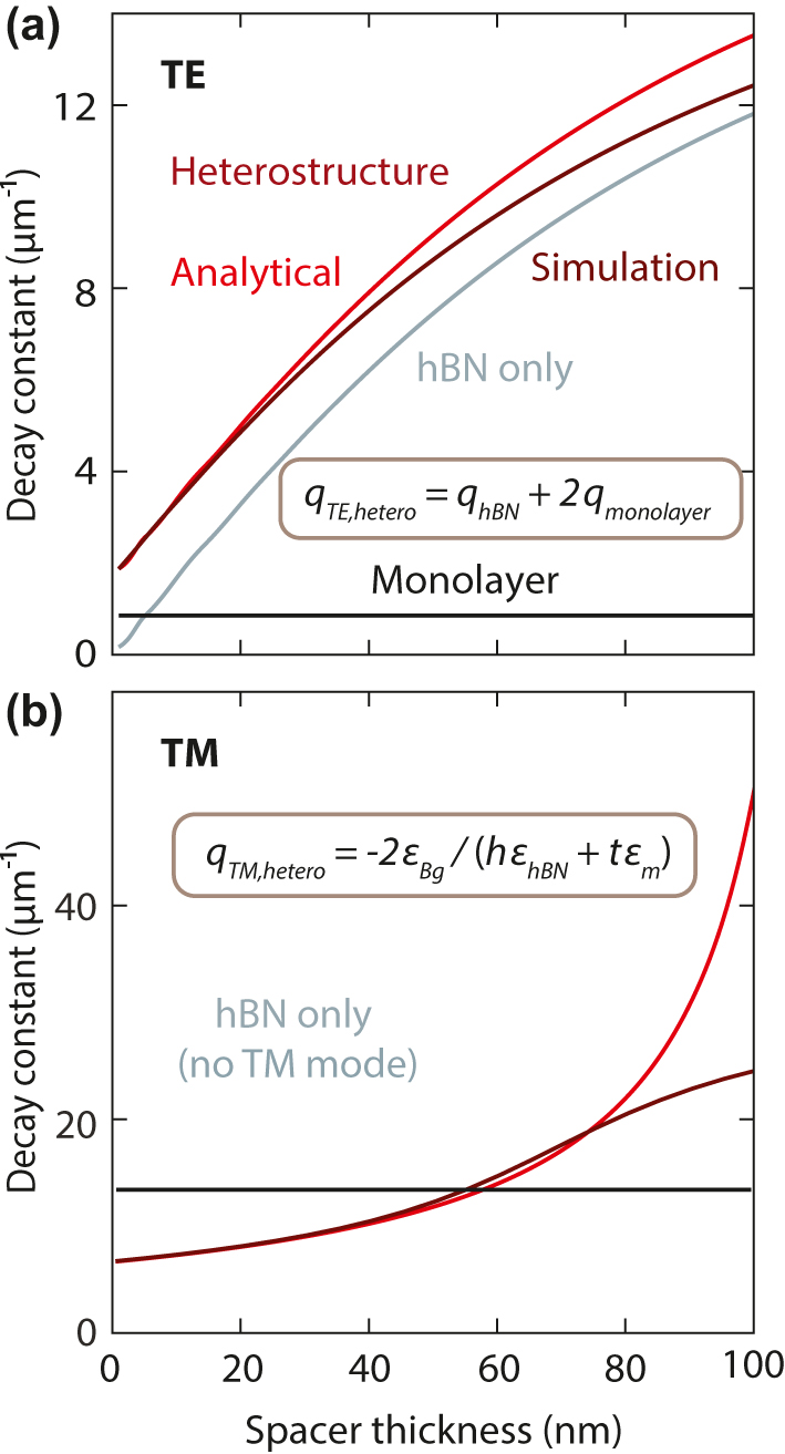
Additivity rules for the decay constants of the guided modes in a heterostructure. Comparison between the decay constant obtained from numerical simulations (dark red) and the theoretically calculated decay constant (red) using the analytical additivity rules for (a) the TE mode at E = 2 eV, and (b) the TM mode at E = 2.0223 eV. Both modes show excellent agreement for thin spacers.
We analyze first the behavior of the decay constant for the WS2 monolayer and hBN layers alone. The decay constant for the monolayer is a horizontal black line in Figure 4(a) and (b), as there is no spacer. If we consider an hBN film only, it supports a TE mode with increasing confinement for increasing thickness (gray line in Figure 4(a)). Conversely, the TM mode is absent for hBN alone at this photon energy due to its positive refractive index (no gray line in Figure 4(b)). For complete heterostructures containing both WS2 and hBN, we observe an excellent agreement between the decay constants obtained using the analytical additivity rules (red lines in Figure 4(a) and (b)) and the numerically simulated decay constants (dark red), particularly for small thicknesses below a few tens of nanometers.
5 Engineering the guided modes in superlattices
A superlattice geometry – a heterostructure stack – can further improve the mode confinement and make the SEP properties more appealing for nanophotonics. The TE mode moves away from the light line for superlattices, providing higher confinement for an increasing number of monolayers (Figure 5(a) and (b)). The effective TE-mode width is 1.2, 0.5, and 0.3 μm for one, two, and three monolayers, respectively. The TM-mode width at E = 2.023 eV rises to 100 nm with three monolayers, suggesting reduced confinement of the TM mode within the structure. The dispersion line moves away from the exciton peak energy as we go from one to three monolayers (Figure 5(a) and (b)).
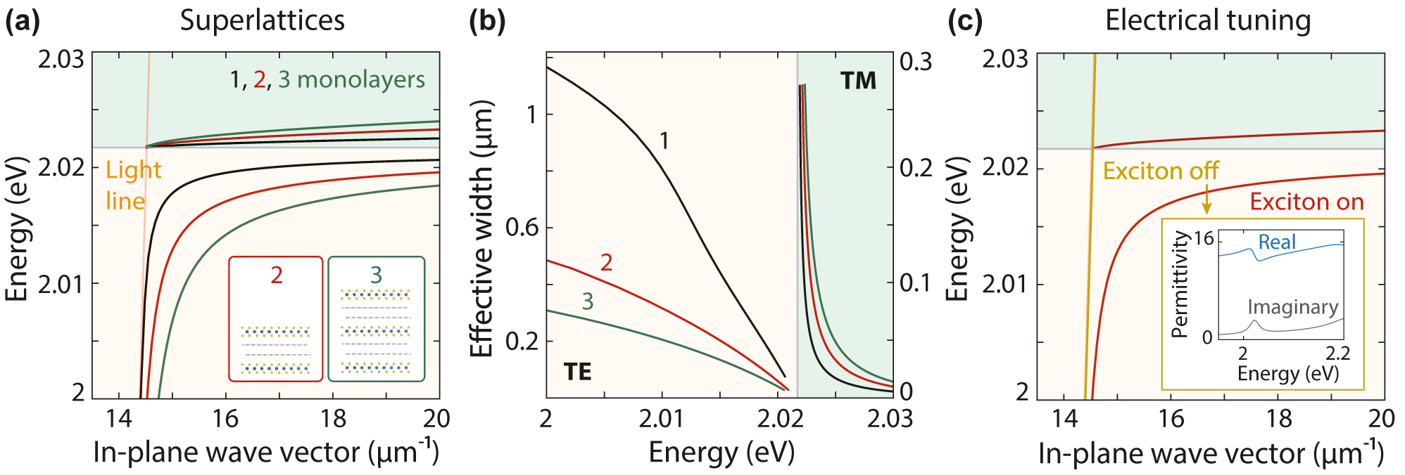
Engineering the dispersion of guided modes in superlattices. (a) Superlattices of WS2 monolayers in stacked heterostructures with hBN spacer thickness of 1 nm and a symmetric PDMS environment. In-plane wave vector as a function of mode energy for structures with one (black), two (red), and three semiconductor monolayers (green). (b) Comparison of the effective widths of the structures in (a), showing a modal compression (TE) or expansion (TM) as the number of layers increases. (c) Predicted tunability when the exciton peak is electrically weakened in a heterostructure comprising two WS2 monolayers and a 1-nm hBN spacer surrounded by PDMS. The TE mode evolves from a confined (red) to a radiation-dominated wave (gold). The TM mode cannot be supported in the absence of a strong exciton. Inset: In-plane permittivity when the exciton is off.
To exploit the advantageous tunability of SEPs, we evaluate how the electrical control of the A exciton can allow active tuning of the guided mode. The refractive index of monolayer TMDs can be tuned using electrical gating; carrier injection can tune and broaden the in-plane permittivity around the exciton resonance [23]. To incorporate tunability in our simulations, we suppress the excitonic behavior of the WS2 monolayers by reducing the oscillator strength from 1.6 to 0.1 eV2, resulting in a drop of ∼50 % of its original permittivity near the A exciton (Figure 5(c), inset). Although electrical doping can induce a slight shift in the exciton resonance energy, accompanied by linewidth broadening [23], such a shift would not qualitatively alter the dispersion calculations. We thus simplify the tuning process by adjusting the oscillator strength alone, as it has a more pronounced impact on our calculations. With this modified permittivity, we can control and potentially modulate the guided modes (Figure 5(c)). The TE mode confinement is frustrated in the heterostructure after suppressing the exciton by turning it toward the light line. Simultaneously, electrical tuning eliminates the possibility of sustaining the TM mode altogether because the permittivity is now positive in the energy range where a strong exciton produced a negative permittivity. Therefore, both modes show promise for modulation.
6 Approaches to solve the dispersion relation: complex β and complex ω
The conditions under which SEPs can be observed in heterostructures depend on the experimental configuration. The governing equations of the guided modes are defined in the complex plane. Consequently, it is possible to solve the dispersion relation by finding the zeros of the transfer-matrix element M 22 in the complex-wave-vector plane or the complex-frequency plane, while keeping the other parameter real (see Methods) [40], [41], [42]. The complex-β and complex-ω approaches lead to different dispersion relations and describe different experimental conditions for polariton excitation [41]. The complex-β approach is suitable when the excitation is a monochromatic wave localized in space [40], [43], [44], [45], whereas a complex ω describes better pulsed or broadband excitation at a fixed angle [46], [47], [48], [49], [50]. In all our results so far, we solved the guided modes using the complex-ω approach. Here, we compare the dispersion relations obtained using the complex-β and complex-ω approaches.
For the complex-ω solutions, we observe an asymptote for large values of β for the TE and TM modes (Figure 6(a), gray lines). Instead, for the complex-β approach at a given real ω (purple lines), the dispersion relation of the TE mode shows a back-bending limiting the maximum value of β. We remove the unphysical branches from the complex-β results because physically meaningful solutions should have real and imaginary parts of the wave vector with the same sign. The TM-mode dispersion lines occur within different energy ranges with a shift between complex-β and complex-ω solutions. The reason for this shift is that when we keep ω as a real value and solve the mode equation, the obtained β values possess a significant imaginary part for the TM mode. However, enforcing a real β requires the film permittivity to be strongly negative. Negative permittivity only occurs near the exciton, which shifts the obtained real part of ω closer to the exciton peak. We also compare the spacer thickness dependence of the guided modes using both approaches. While the TE mode can propagate for any spacer thickness, we obtain a cutoff thickness for the TM mode for a 1-nm hBN spacer (Supplementary Section S6). Above this thickness, the effective total permittivity of the stack becomes positive, and no TM mode is supported.
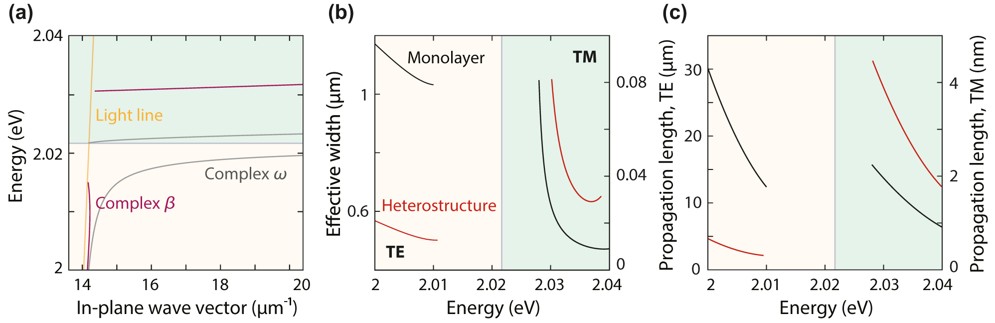
Dispersion relations in the complex-wave-vector and complex-frequency approaches. (a) Mode dispersion in a heterostructure obtained using the complex-β approach (purple) compared to the complex-ω approach (gray), corresponding to different experimental situations. Unphysical branches are not shown in the dispersion diagram. The heterostructure consists of two WS2 monolayers separated by a 0.3-nm-thick hBN monolayer in a symmetric PDMS environment. (b and c) Effective width and propagation length obtained by using the complex-β approach for both guided modes in the same heterostructure and in a monolayer.
Focusing on specific energies, we observe a similar evolution of the effective mode width for both approaches (Figure 6(b)). For complex β, the TE mode at E = 2 eV is confined to around 0.55 μm for the heterostructure (red) compared to 1.15 μm for the monolayer (black), whereas the TM mode at E = 2.03 eV expands from 30 nm for the monolayer to 80 nm for the heterostructure. Additionally, the complex-β approach allows us to calculate an additional SEP property: the propagation length,
Finally, we demonstrate the effect of the exciton linewidth γ A , which can be controlled by lowering the temperature [51], [52], on the different modes in our heterostructures. We show that decreasing the linewidth (or increasing the oscillator strength) is particularly beneficial for complex-β solutions of both TE and TM modes. We vary the A-exciton linewidth in our 4-Lorentzian permittivity model and calculate the SEP dispersion curve for γ A = 22.7 (experimentally retrieved value at room temperature), 15, 10, and 5 meV (Figure 7). The TE mode has a more pronounced back-bending line and higher confinement using the narrowest linewidth, underscoring the need for high-quality excitons and possibly low temperatures to ease observation in experiments described by the complex-β approach [32]. In the complex-ω approach, adjustments to the linewidth do not significantly affect the dispersion. However, the propagation length exhibits changes because modifying the linewidth causes a shift in the permittivity in the complex plane, bringing it closer to the real axis.
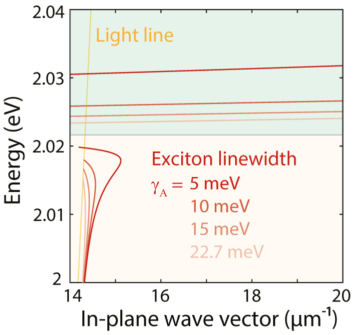
Enhanced confinement for decreasing exciton linewidth γ A . Exciton–polariton dispersion for a heterostructure obtained using the complex-β approach for linewidths γ A = 5, 10, 15, and 22.7 meV, demonstrating the crucial role played by the exciton quality. The heterostructure consists of two WS2 monolayers separated by a 0.3-nm-thick hBN spacer (i.e., one monolayer) in a symmetric PDMS environment.
7 Conclusions
We have investigated surface exciton–polaritons supported by atomically thin semiconductor–insulator–semiconductor heterostructures and their superlattices. These guided waves rely on the presence of strong exciton resonances with a high oscillator strength and narrow linewidth, as provided by WS2 monolayers even at room temperature. The observation of these modes also requires a symmetric optical environment. Both TE and TM modes are possible for high-quality monolayers within spectral ranges characterized by positive and negative permittivities, respectively. Compared to the monolayer modes, the heterostructure architecture modifies and controls the exciton–polariton confinement, effective width, wavelength, and propagation length. Increasing the insulator spacer thickness provides higher confinement for both TE and TM modes. Similarly, using heterostructures incorporating a larger number of monolayers and ultrathin spacers can further increase the TE mode confinement while resulting in a more delocalized TM mode. We proposed strongly controlling and modulating the guided modes by switching the monolayer excitons on and off. Finally, we have shown that surface exciton–polariton waves can be predicted with either a complex-wave-vector or a complex-frequency approach. These two approaches provide qualitatively different mode dispersions and properties. As they describe different experimental conditions, it is critical to consider the most appropriate complex-plane approach to model a specific experiment.
Our results offer substantial practical advantages in the use of surface exciton–polariton waves supported by monolayer semiconductors. TE modes have previously required a closely symmetric refractive index environment as well as patterning to achieve the necessary confinement for experimental detection. Our approach faciliates the observation of surface-exciton polaritons by enhancing confinement without the need for patterning, potentially enabling widespread implementation and broader applications. For TM modes, which have not been observed yet experimentally in semiconductor monolayers, our findings suggest that their reduced confinement could result in longer propagation lengths. However, our approach may also require greater complexity in fabrication and alignment compared to monolayer systems. In addition, the diverse tuning mechanisms of excitons in monolayer semiconductors provide a control knob for guided waves based on changes to the exciton strength, linewidth, and peak energy. For example, all-optical modulation due to lattice heating has been shown to substantially alter the reflectivity of atomically thin mirrors [22] and could be used to modulate exciton–polaritons in space and time. Based on our results and given the fast pace of developments in this area, we argue that atomically thin semiconductors hold great promise for nanoscale tunable photonics at visible wavelengths.
8 Methods
8.1 Transfer-matrix method
In our study of surface exciton–polaritons in semiconductor–insulator–semiconductor heterostructures, we employ the transfer-matrix method to theoretically analyze and simulate the propagation of electromagnetic waves at the interfaces between different media. We start by considering two different media separated by a planar interface. The forward and backward wave amplitudes in medium 1 are denoted by A
1 and B
1, respectively. Similarly, A
2 and B
2 are the waves in medium 2. The interface transfer matrix connects the amplitudes of the waves in the two media through
By applying the electric- and magnetic-field boundary conditions depending on the polarization of the wave (TE or TM), we can evaluate the matrix elements M
ij
, which depend on the optical properties of the layered medium. For the TE mode, we obtain
The propagation transfer matrix in a homogeneous medium is
This method remains applicable for both complex-ω and complex-β approaches. The complex-ω approach involves finding ω for each real value of β using a permittivity defined in the complex-ω plane. The obtained ω from the mode solution is used to extend the permittivity in the complex-ω plane using the 4-Lorentzian model (Supplementary Sections S1 and S3). Consequently, the permittivity for the complex-ω approach encompasses two branches, one for the TE mode and another for the TM mode, each of them requiring the determination of complex ω values independently. Likewise, the complex-β approach relies on finding the real and imaginary parts of β with a permittivity defined at each real ω.
Funding source: Exacte en Natuurwetenschappen
Award Identifier / Grant number: 024.002.033
Award Identifier / Grant number: 740.018.009
Acknowledgments
We thank Rasmus H. Godiksen, Shaojun Wang, and Ershad Mohammadi for assistance and stimulating discussions.
-
Research funding: This work was financially supported by the Netherlands Organisation for Scientific Research (NWO) through an NWO START-UP grant (740.018.009) and the Gravitation grant “Research Centre for Integrated Nanophotonics” (024.002.033).
-
Author contributions: All authors have accepted responsibility for the entire content of this manuscript and approved its submission.
-
Conflict of interest: The authors state no conflicts of interest.
-
Data availability: The datasets generated and/or analyzed during the current study are available from the corresponding author upon reasonable request.
References
[1] D. N. Basov, M. M. Fogler, and F. J. García De Abajo, “Polaritons in van der Waals materials,” Science, vol. 354, no. 6309, p. aag1992, 2016. https://doi.org/10.1126/science.aag1992.Suche in Google Scholar PubMed
[2] A. V. Zayats, I. I. Smolyaninov, and A. A. Maradudin, “Nano-optics of surface plasmon polaritons,” Phys. Rep., vol. 408, nos. 3–4, pp. 131–314, 2005. https://doi.org/10.1016/j.physrep.2004.11.001.Suche in Google Scholar
[3] J.-C. Weeber, J. R. Krenn, A. Dereux, B. Lamprecht, Y. Lacroute, and J. P. Goudonnet, “Near-field observation of surface plasmon polariton propagation on thin metal stripes,” Phys. Rev. B, vol. 64, no. 4, p. 045411, 2001. https://doi.org/10.1103/physrevb.64.045411.Suche in Google Scholar
[4] F. Yang, J. R. Sambles, and G. W. Bradberry, “Long-range coupled surface exciton polaritons,” Phys. Rev. Lett., vol. 64, no. 5, p. 559, 1990. https://doi.org/10.1103/physrevlett.64.559.Suche in Google Scholar PubMed
[5] F. Yang, G. W. Bradberry, and J. R. Sambles, “Experimental observation of surface exciton-polaritons on vanadium using infrared radiation,” J. Mod. Opt., vol. 37, no. 9, pp. 1545–1553, 1990. https://doi.org/10.1080/09500349014551721.Suche in Google Scholar
[6] I. Hirabayashi, T. Koda, Y. Tokura, J. Murata, and Y. Kaneko, “Surface exciton-polariton in CuBr,” J. Phys. Soc. Jpn., vol. 40, no. 4, pp. 1215–1216, 1976. https://doi.org/10.1143/jpsj.40.1215.Suche in Google Scholar
[7] Y. Tokura and T. Koda, “Surface exciton polariton in ZnO,” J. Phys. Soc. Jpn., vol. 51, no. 9, pp. 2934–2946, 1982. https://doi.org/10.1143/jpsj.51.2934.Suche in Google Scholar
[8] M. S. Bradley, J. R. Tischler, and V. Bulović, “Layer-by-layer J-aggregate thin films with a peak absorption constant of 106 cm-1,” Adv. Mater., vol. 17, no. 15, pp. 1881–1886, 2005. https://doi.org/10.1002/adma.200500233.Suche in Google Scholar
[9] M. J. Gentile, S. Núñez-Sánchez, and W. L. Barnes, “Optical field-enhancement and subwavelength field-confinement using excitonic nanostructures,” Nano Lett., vol. 14, no. 5, pp. 2339–2344, 2014. https://doi.org/10.1021/nl404712t.Suche in Google Scholar PubMed
[10] Y. Xu, L. Wu, and L. K. Ang, “Surface exciton polaritons: a promising mechanism for refractive-index sensing,” Phys. Rev. Appl., vol. 10, no. 2, p. 24029, 2019. https://doi.org/10.1103/physrevapplied.12.024029.Suche in Google Scholar
[11] K. F. Mak, K. He, J. Shan, and T. F. Heinz, “Control of valley polarization in monolayer MoS2 by optical helicity,” Nat. Nanotechnol., vol. 7, no. 8, pp. 494–498, 2012. https://doi.org/10.1038/nnano.2012.96.Suche in Google Scholar PubMed
[12] T. Cao, et al.., “Valley-selective circular dichroism of monolayer molybdenum disulphide,” Nat. Commun., vol. 3, p. 887, 2012. https://doi.org/10.1038/ncomms1882.Suche in Google Scholar PubMed PubMed Central
[13] T. Low, et al.., “Polaritons in layered two-dimensional materials,” Nat. Mater., vol. 16, no. 2, pp. 182–194, 2017. https://doi.org/10.1038/nmat4792.Suche in Google Scholar PubMed
[14] Y. Zeng, et al.., “Tailoring topological transitions of anisotropic polaritons by interface engineering in biaxial crystals,” Nano Lett., vol. 22, no. 10, pp. 4260–4268, 2022. https://doi.org/10.1021/acs.nanolett.2c00399.Suche in Google Scholar PubMed
[15] C. Hu, et al.., “Source-configured symmetry-broken hyperbolic polaritons,” eLight, vol. 3, no. 1, p. 14, 2023. https://doi.org/10.1186/s43593-023-00047-1.Suche in Google Scholar
[16] Z. Dai, et al.., “Edge-oriented and steerable hyperbolic polaritons in anisotropic van der Waals nanocavities,” Nat. Commun., vol. 11, p. 6086, 2020. https://doi.org/10.1038/s41467-020-19913-4.Suche in Google Scholar PubMed PubMed Central
[17] L. Ju, et al.., “Graphene plasmonics for tunable terahertz metamaterials,” Nat. Nanotechnol., vol. 6, no. 10, pp. 630–634, 2011. https://doi.org/10.1038/nnano.2011.146.Suche in Google Scholar PubMed
[18] M. Jablan, H. Buljan, and M. Soljačić, “Plasmonics in graphene at infrared frequencies,” Phys. Rev. B, vol. 80, no. 24, p. 245435, 2009. https://doi.org/10.1103/physrevb.80.245435.Suche in Google Scholar
[19] Y. Li, et al.., “Measurement of the optical dielectric function of monolayer transition-metal dichalcogenides: MoS2, MoSe2, WS2, and WSe2,” Phys. Rev. B, vol. 90, no. 20, p. 205422, 2014. https://doi.org/10.1103/PhysRevB.90.205422.Suche in Google Scholar
[20] P. Back, A. Ijaz, S. Zeytinoglu, M. Kroner, and A. Imamoglu, “Realization of an atomically thin mirror using monolayer MoSe2,” Phys. Rev. Lett., vol. 120, no. 3, p. 037401, 2017. https://doi.org/10.1103/physrevlett.120.037401.Suche in Google Scholar
[21] F. Ferreira, A. J. Chaves, N. M. R. Peres, and R. M. Ribeiro, “Excitons in hexagonal boron nitride single-layer: a new platform for polaritonics in the ultraviolet,” J. Opt. Soc. Am. B, vol. 36, no. 3, p. 674, 2019. https://doi.org/10.1364/josab.36.000674.Suche in Google Scholar
[22] G. Scuri, et al.., “Large excitonic reflectivity of monolayer MoSe2 encapsulated in hexagonal boron nitride,” Phys. Rev. Lett., vol. 120, no. 3, p. 037402, 2018. https://doi.org/10.1103/physrevlett.120.037402.Suche in Google Scholar
[23] Y. Yu, L. Huang, H. Peng, L. Xiong, and L. Cao, “Giant gating tunability of optical refractive index in transition metal dichalcogenide monolayers,” Nano Lett., vol. 17, no. 6, pp. 3613–3618, 2017. https://doi.org/10.1021/acs.nanolett.7b00768.Suche in Google Scholar PubMed
[24] P. Back, S. Zeytinoglu, A. Ijaz, M. Kroner, and A. Imamoǧlu, “Realization of an electrically tunable narrow-bandwidth atomically thin mirror using monolayer MoSe2,” Phys. Rev. Lett., vol. 120, no. 3, p. 037401, 2018. https://doi.org/10.1103/physrevlett.120.037401.Suche in Google Scholar
[25] A. Pal and D. A. Huse, “Many-body localization phase transition,” Phys. Rev. B, vol. 82, no. 17, p. 174411, 2010. https://doi.org/10.1103/physrevb.82.174411.Suche in Google Scholar
[26] V. Karanikolas, I. Thanopulos, and E. Paspalakis, “Strong interaction of quantum emitters with a WS2 layer enhanced by a gold substrate,” Opt. Lett., vol. 44, no. 8, pp. 2049–2052, 2019. https://doi.org/10.1364/ol.44.002049.Suche in Google Scholar PubMed
[27] G. T. Papadakis, A. Davoyan, P. Yeh, and H. A. Atwater, “Mimicking surface polaritons for unpolarized light with high-permittivity materials,” Phys. Rev. Mater., vol. 3, no. 1, p. 015202, 2019. https://doi.org/10.1103/physrevmaterials.3.015202.Suche in Google Scholar
[28] V. D. Karanikolas, C. A. Marocico, P. R. Eastham, and A. L. Bradley, “Near-field relaxation of a quantum emitter to two-dimensional semiconductors: surface dissipation and exciton polaritons,” Phys. Rev. B, vol. 94, no. 19, p. 195418, 2016. https://doi.org/10.1103/physrevb.94.195418.Suche in Google Scholar
[29] J. B. Khurgin, “Two-dimensional exciton–polariton—light guiding by transition metal dichalcogenide monolayers,” Optica, vol. 2, no. 8, pp. 740–742, 2015. https://doi.org/10.1364/optica.2.000740.Suche in Google Scholar
[30] X. Zhang, et al.., “Guiding of visible photons at the ångström thickness limit,” Nat. Nanotechnol., vol. 14, no. 8, pp. 844–850, 2019. https://doi.org/10.1038/s41565-019-0519-6.Suche in Google Scholar PubMed
[31] M. Lee, et al.., “Wafer-scale δ waveguides for integrated two-dimensional photonics,” Science, vol. 381, no. 6658, pp. 648–653, 2023. https://doi.org/10.1126/science.adi2322.Suche in Google Scholar PubMed
[32] I. Epstein, et al.., “Highly confined in-plane propagating exciton-polaritons on monolayer semiconductors,” 2D Mater., vol. 7, no. 3, p. 035031, 2020. https://doi.org/10.1088/2053-1583/ab8dd4.Suche in Google Scholar
[33] S. Eizagirre Barker, et al.., “Preserving the emission lifetime and efficiency of a monolayer semiconductor upon transfer,” Adv. Opt. Mater., vol. 7, no. 13, p. 1900351, 2019. https://doi.org/10.1002/adom.201900351.Suche in Google Scholar
[34] S. Wang, et al.., “Limits to strong coupling of excitons in multilayer WS2 with collective plasmonic resonances,” ACS Photonics, vol. 6, no. 2, pp. 286–293, 2019. https://doi.org/10.1021/acsphotonics.8b01459.Suche in Google Scholar
[35] E. J. Sie, et al.., “Observation of exciton redshift-blueshift crossover in monolayer WS2,” Nano Lett., vol. 17, no. 7, pp. 4210–4216, 2017. https://doi.org/10.1021/acs.nanolett.7b01034.Suche in Google Scholar PubMed
[36] B. Sun, C. Cai, and B. Seshasayee Venkatesh, “Matrix method for two-dimensional waveguide mode solution,” J. Mod. Opt., vol. 65, no. 8, pp. 914–919, 2018. https://doi.org/10.1080/09500340.2017.1414896.Suche in Google Scholar
[37] J. Madrigal-Melchor, J. S. Pérez-Huerta, J. R. Suárez-López, I. Rodríguez-Vargas, and D. Ariza-Flores, “TM plasmonic modes in a multilayer graphene-dielectric structure,” Superlattices Microstruct., vol. 125, pp. 247–255, 2019. https://doi.org/10.1016/j.spmi.2018.11.015.Suche in Google Scholar
[38] Y. Li, et al.., “Revealing low-loss dielectric near-field modes of hexagonal boron nitride by photoemission electron microscopy,” Nat. Commun., vol. 14, p. 4837, 2023. https://doi.org/10.1038/s41467-023-40603-4.Suche in Google Scholar PubMed PubMed Central
[39] S. Y. Lee, T. Y. Jeong, S. Jung, and K. J. Yee, “Refractive index dispersion of hexagonal boron nitride in the visible and near-infrared,” Phys. Status Solidi B, vol. 256, no. 6, p. 1800417, 2019. https://doi.org/10.1002/pssb.201800417.Suche in Google Scholar
[40] E. T. Arakawa, M. W. Williams, R. N. Hamm, and R. H. Ritchie, “Effect of damping on surface plasmon dispersion,” Phys. Rev. Lett., vol. 31, no. 18, pp. 1127–1129, 1973. https://doi.org/10.1103/physrevlett.31.1127.Suche in Google Scholar
[41] A. Archambault, T. V. Teperik, F. Marquier, and J. J. Greffet, “Surface plasmon Fourier optics,” Phys. Rev. B, vol. 79, no. 19, p. 195414, 2009. https://doi.org/10.1103/physrevb.79.195414.Suche in Google Scholar
[42] I. B. Udagedara, I. D. Rukhlenko, and M. Premaratne, “Complex-ω approach versus complex-k approach in description of gain-assisted surface plasmon-polariton propagation along linear chains of metallic nanospheres,” Phys. Rev. B, vol. 83, no. 15, p. 115451, 2011. https://doi.org/10.1103/physrevb.83.115451.Suche in Google Scholar
[43] E. Schuller, H. J. Falge, and G. Borstel, “Dispersion curves of surface phonon-polaritons with backbending,” Phys. Lett. A, vol. 54, no. 4, pp. 317–318, 1975. https://doi.org/10.1016/0375-9601(75)90275-3.Suche in Google Scholar
[44] F. Hu, et al.., “Imaging exciton-polariton transport in MoSe2 waveguides,” Nat. Photonics, vol. 11, no. 5, pp. 356–360, 2017. https://doi.org/10.1038/nphoton.2017.65.Suche in Google Scholar
[45] F. Hu, et al.., “Imaging propagative exciton polaritons in atomically thin WSe2 waveguides,” Phys. Rev. B, vol. 100, no. 12, p. 121301, 2019. https://doi.org/10.1103/physrevb.100.121301.Suche in Google Scholar
[46] Q. Wang, L. Sun, B. Zhang, C. Chen, X. Shen, and W. Lu, “Direct observation of strong light-exciton coupling in thin WS2 flakes,” Opt. Express, vol. 24, no. 7, p. 7151, 2016. https://doi.org/10.1364/oe.24.007151.Suche in Google Scholar PubMed
[47] S. Dufferwiel, et al.., “Exciton-polaritons in van der Waals heterostructures embedded in tunable microcavities,” Nat. Commun., vol. 6, p. 8579, 2015. https://doi.org/10.1038/ncomms9579.Suche in Google Scholar PubMed PubMed Central
[48] L. C. Flatten, et al.., “Room-temperature exciton-polaritons with two-dimensional WS2,” Sci. Rep., vol. 6, p. 33134, 2016. https://doi.org/10.1038/srep33134.Suche in Google Scholar PubMed PubMed Central
[49] L. Zhang, R. Gogna, W. Burg, E. Tutuc, and H. Deng, “Photonic-crystal exciton-polaritons in monolayer semiconductors,” Nat. Commun., vol. 9, p. 713, 2018. https://doi.org/10.1038/s41467-018-03188-x.Suche in Google Scholar PubMed PubMed Central
[50] P. T. Kristensen, K. Herrmann, F. Intravaia, and K. Busch, “Modeling electromagnetic resonators using quasinormal modes,” Adv. Opt. Photon, vol. 12, no. 3, pp. 612–708, 2020. https://doi.org/10.1364/aop.377940.Suche in Google Scholar
[51] F. Cadiz, et al.., “Excitonic linewidth approaching the homogeneous limit in MoS2-based van der Waals heterostructures,” Phys. Rev. X, vol. 7, no. 2, p. 021026, 2017. https://doi.org/10.1103/physrevx.7.021026.Suche in Google Scholar
[52] M. Selig, et al.., “Excitonic linewidth and coherence lifetime in monolayer transition metal dichalcogenides,” Nat. Commun., vol. 7, p. 13279, 2016. https://doi.org/10.1038/ncomms13279.Suche in Google Scholar PubMed PubMed Central
Supplementary Material
This article contains supplementary material (https://doi.org/10.1515/nanoph-2024-0075).
© 2024 the author(s), published by De Gruyter, Berlin/Boston
This work is licensed under the Creative Commons Attribution 4.0 International License.
Artikel in diesem Heft
- Frontmatter
- Reviews
- Deep learning for optical tweezers
- Lithium niobate on insulator – fundamental opto-electronic properties and photonic device prospects
- Research Articles
- Aberration-corrected hybrid metalens for longwave infrared thermal imaging
- Adaptive fabric with emissivity regulation for thermal management of humans
- Frequency down-conversion of terahertz waves at optically induced temporal boundaries in GaAs waveguides
- Continuously tuneable single electrode pair liquid crystal optical vortex generators
- Guiding light with surface exciton–polaritons in atomically thin superlattices
- Noninvasive inset-integrated meta-atom for achieving single-layer metasurface simultaneously with coded microwave reflectivity and digitalized infrared emissivity
- Visible-infrared compatible and independent camouflage with multicolor patterns and tunable emissivity
- Capillary-assisted flat-field formation: a platform for advancing nanoparticle tracking analysis in an integrated on-chip optofluidic environment
- Enhancing metasurface fabricability through minimum feature size enforcement
- Enhancement of third-harmonic generation in all-dielectric kite-shaped metasurfaces driven by quasi-bound states in the continuum
- Multispectral metal-based electro-optical metadevices with infrared reversible tunability and microwave scattering reduction